UNIVERSIDADE DO ALGARVE
INSTITUTO SUPERIOR DE ENGENHARIA
Aging Monitoring Methodology for
Built-In Self-Test Applications
Metodologia de Monitorização do Envelhecimento
para Aplicações de Auto-teste Embutido
João Ricardo dos Santos Coelho
Dissertação para obtenção do Grau de Mestre em Engenharia Eléctrica e Electrónica
Área de Especialização em Tecnologias de Informação e Telecomunicações
Orientador: Professor Doutor Jorge Filipe Leal Costa Semião
i
Aging Monitoring Methodology for
Built-In Self-Test Applications
Declaração de autoria de trabalho
Declaro ser o autor deste trabalho, que é original e inédito. Autores e trabalhos consultados estão devidamente citados no texto e constam da listagem de referências incluída.
Assinatura:
Copyright © João Ricardo dos Santos Coelho
A Universidade do Algarve tem o direito, perpétuo e sem limites geográficos, de arquivar e publicitar este trabalho através de exemplares impressos reproduzidos em papel ou de forma digital, ou por qualquer outro meio conhecido ou que venha a ser inventado, de o divulgar através de repositórios científicos e de admitir a sua cópia e distribuição com objectivos educacionais ou de investigação, não comerciais, desde que seja dado crédito ao autor e editor.
iii
v
A
CKNOWLEDGMENTSThis study is not only the result of an individual effort, but rather a set of efforts that made it possible and without them it would have been much more difficult to reach the end of this step, which represents an important milestone in my personal and professional life. Therefore, I express my gratitude to all those who were present at complex times.
To Professor Jorge Semião, in particular, I want to express my thanks for the guidance printed to the whole process, combining the stamp of high scientific standards, an abiding and fruitful interest, which helped to catalyze the present investigation. I also want to highlight the critical, objective and motivated vision, dedicated to the pursuit and constant improvement of this thesis.
To my daughter and to my wife, who during these years have been a constant support and encouragement, I want to express a word of thanks for the consideration, generosity and affection, contributing to tread this path until the end and to all my family, who encouraged me in the decision to start, continue and complete this project, and made me taste the true solidarity, when it showed the complex challenge of ensuring the link between family roles, and professional research.
I thank also to my colleague and friend Engº Vasco Fernandes, for sharing again your motivator character in times of special relevance. And to my colleague and friend Engº Hugo Cavalaria, who helped me in important areas like VHDL, making faster and effective my learning process in a relevant area to the development of this work.
Finally, to all who have provided documentation and miscellaneous information, I also want to leave a word of thanks.
vii
A
BSTRACTThe high integration level achieved as well as complexity and performance enhancements in new nanometer technologies make IC (Integrated Circuits) products very difficult to test. Moreover, long term operation brings aging cumulative degradations, due to new processes and materials that lead to emerging defect phenomena and the consequence are products with increased variability in their behaviour, more susceptible to delay-faults and with a reduced expected lifecycle.
The main objectives of this thesis are twofold, as explained in the following. First, a new software tool is presented to generate HDL (Hardware Description Language) for BIST (Built-In Self-Test) structures, aiming delay-faults, and inserted the new auto-test functionality in generic sequential CMOS circuits. The BIST methodology used implements a scan based BIST approach, using a new BIST controller to implement the Launch-On-Shift (LOS) and Launch-On-Capture (LOC) delay-fault techniques.
Second, it will be shown that multi-VDD tests in circuits with BIST
infra-structures can be used to detect gross delay-faults during on-field operations, and consequently can be used as an aging sensor methodology during circuits’ lifecycle.
The discrete set of multi-VDD BIST sessions generates a Voltage Signature Collection
(VSC) and the presence of a delay-fault (or a physical defect) modifies the VSC collection, allowing the aging sensor capability.
The proposed Design for Testability (DFT) method and tool are demonstrated with extensive SPICE simulation using three ITC’99 benchmark circuits.
Keywords: Built-In Self-Test, Aging Sensor Methodology, Multi-VDD Tests, HDL
ix
R
ESUMOO elevado nível de integração atingida, complexidade, assim como performances melhoradas em novas tecnologias nanométricas tornam os produtos em circuitos integrados tecnológicos muito difíceis de testar. Para além disso, a operação a longo prazo produz degradações cumulativas pelo envelhecimento dos circuitos, devido a novos processos e materiais que conduzem a novos defeitos e a consequência são produtos com maior variabilidade no seu funcionamento, mais susceptíveis às faltas de atraso e com um tempo de vida menor.
Os principais objectivos desta tese são dois, como explicado em seguida. Primeiro, é apresentada uma nova ferramenta de software para gerar estruturas de auto-teste integrado (BIST, Built-In Self-Test) descritas em linguagens de descrição de
hardware (HDL, Hardware Description Language), com o objectivo de detectar faltas
de atraso, e inserir a nova funcionalidade de auto-teste em circuitos genéricos sequenciais CMOS. A metodologia de BIST utilizada implementa um procedimento baseado em caminhos de deslocamento, utilizando um novo controlador de BIST para implementar técnicas de faltas de atraso, como Shift (LOS) e
Launch-On-Capture (LOC).
Segundo, irá ser mostrado que testes multi-VDD em circuitos com
infra-estruturas de BIST podem ser usados para detectar faltas de atraso grosseiras durante a operação no terreno e, consequentemente, pode ser usado como uma metodologia de sensor de envelhecimento durante o tempo de vida dos circuitos. Um número discreto
de sessões BIST multi-VDD geram uma Colecção de Assinaturas de Tensão (Voltage
Signature Collection, VSC) e a presença de uma falta de atraso (ou um defeito físico)
faz modificar a colecção VSC, comportando-se como sensor de envelhecimento.
O trabalho foi iniciado com o estudo do estado da arte nesta área. Assim, foram estudadas e apresentadas no capítulo 2 as principais técnicas de DfT (Design for
Testability) disponíveis e utilizadas pela indústria, nomeadamente, as técnicas de SP
(Scan Path), de BIST e as técnicas de scan para delay-faults, LOS e LOC. No capítulo 3, ainda referente ao estudo sobre o estado da arte, é apresentado o estudo sobre os
fenómenos que provocam o envelhecimento dos circuitos digitais, nomeadamente o
NBTI (Negative Bias Temperature Instability), que é considerado o factor mais
relevante no envelhecimento de circuitos integrados (especialmente em nanotecnologias).
Em seguida, iniciou-se o desenvolvimento do primeiro objectivo. Relativamente a este assunto, começou-se por definir qual o comportamento das estruturas de BIST e como se iriam interligar. O comportamento foi descrito, bloco a bloco, em VHDL comportamental, ao nível RTL (Register Transfer Level). Esta descrição foi então validada por simulação, utilizando a ferramenta ModelSim. Posteriormente, esta descrição comportamental foi sintetizada através da ferramenta
Synopsys, com a colaboração do INESC-ID em Lisboa (instituição parceira nestes
trabalhos de investigação), e foi obtida uma netlist ao nível de porta lógica, que foi guardada utilizando a linguagem de descrição de hardware Verilog. Assim, obtiveram-se dois tipos de descrição dos circuitos BIST: uma comportamental, em
VHDL, e outra estrutural, em Verilog (esta descrição estrutural em Verilog irá
permitir, posteriormente, fazer a simulação e análise de envelhecimento).
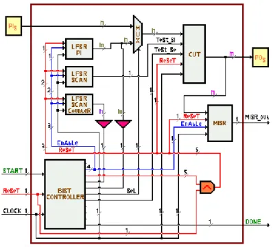
A nova estrutura de BIST obtida é baseada no modelo clássico de BIST, mas apresenta algumas alterações, nomeadamente ao nível da geração de vectores de teste e no controlo e aplicação desses vectores ao circuito. Estas modificações têm como objectivo aumentar a detecção de faltas e permitir o teste de faltas de atraso. É composto por três blocos denominados LFSRs (Linear Feedback Shift Registers), um utilizado para gerar os vectores pseudo-aleatórios para as entradas primárias do circuito, outro para gerar os vectores para a entrada do scan path, e o último utilizado como contador para controlar o número de bits introduzidos no scan path. Relativamente ao controlador, este foi especificamente desenhado para controlar um teste com estratégia de test-per-scan (ou seja, um teste baseado no caminho de varrimento existente no circuito) e tem uma codificação de estados que permite implementar as estratégias de teste de faltas de atraso, Launch-On-Shift (LOS) e
Launch-On-Capture (LOC). Na secção de saída do novo modelo de BIST, o processo
de compactação usa o mesmo princípio do modelo tradicional, utilizando neste caso um MISR (Multiple Input Signature Register).
Ainda relativamente ao primeiro objectivo, seguiu-se o desenvolvimento da ferramenta BISTGen, para automatizar a geração das estruturas de BIST atrás
mencionadas, nos dois tipos de descrição, e automaticamente inserir estas estruturas num circuito de teste (CUT, Circuit Under Test). A aplicação de software deve permitir o manuseamento de dois tipos de informação relativa ao circuito: descrição do circuito pelo seu comportamento, em VHDL, e descrição do circuito pela sua estrutura, em Verilog. Deve ter como saída a descrição de hardware supra citada, inserindo todos os blocos integrantes da estrutura num só ficheiro, contendo apenas um dos tipos de linguagem (Verilog ou VHDL), escolhida previamente pelo utilizador. No caso dos LFSRs e do MISR, o programa deve permitir ao utilizador a escolha de
LFSRs do tipo linear ou do tipo modular (também conhecidos por fibonacci ou galois), e deve também possuir suporte para automaticamente seleccionar de uma
base de dados quais as realimentações necessárias que conduzem à definição do polinómio primitivo para o LFSR. Será necessário ainda criar uma estrutura em base de dados para gerir os nomes e o número de entradas e saídas do circuito submetido a teste, a que chamamos CUT, de forma a simplificar o processo de renomeação que o utilizador poderá ter de efectuar. Dar a conhecer ao programa os nomes das entradas e saídas do CUT é de relevante importância, uma vez que a atribuição de nomes para as entradas e saídas pode vir em qualquer língua ou dialecto, não coincidindo com os nomes padrão normalmente atribuídos.
Relativamente às duas linguagens que o programa recebe através do CUT na sua entrada, no caso VHDL após inserir BIST o ficheiro final terá sempre uma estrutura semelhante, qualquer que seja o ficheiro a ser tratado, variando apenas com o hardware apresentado pelo CUT. No entanto, para o caso Verilog a situação será diferente, uma vez que o programa tem de permitir que o ficheiro final gerado possa surgir de duas formas dependendo da escolha desejada. A primeira forma que o
software deve permitir para o caso Verilog é gerar um ficheiro contendo módulos, de uma forma semelhante ao que acontece no caso VHDL. No entanto, deve permitir também a obtenção, caso o utilizador solicite, de um ficheiro unificado, sem sub-módulos nos blocos, para que o ficheiro final contenha apenas uma única estrutura, facilitando a sua simulação e análise de envelhecimento nas etapas seguintes.
Relativamente ao segundo objectivo, com base no trabalho anterior já efectuado em metodologias para detectar faltas de delay em circuitos com BIST, foi definida uma metodologia de teste para, durante a vida útil dos circuitos, permitir
avaliar como vão envelhecendo, tratando-se assim de uma metodologia de monitorização de envelhecimento para circuitos com BIST.
Um aspecto fundamental para a realização deste segundo objectivo é podermos prever como o circuito vai envelhecer. Para realizar esta tarefa, sempre subjectiva, utilizou-se uma ferramenta desenvolvida no ISE-UAlg em outra tese de mestrado anterior a esta, a ferramenta AgingCalc. Esta ferramenta inicia-se com a definição, por parte do utilizador, das probabilidades de operação das entradas primárias do circuito (probabilidades de cada entrada estar a ‘0’ ou a ‘1’). De notar que este é o processo subjectivo existente na análise de envelhecimento, já que é impossível prever como um circuito irá ser utilizado. Com base nestas probabilidades de operação, o programa utiliza a estrutura do circuito para calcular, numa primeira instância, as probabilidades dos nós do circuito estarem a ‘0’ ou a ‘1’, e numa segunda instância as probabilidades de cada transístor PMOS estar ligado e com o seu canal
em stress (com uma tensão negativa aplicada à tensão VGS e um campo eléctrico
aplicado ao dieléctrico da porta). Utilizando fórmulas definidas na literatura para modelação do parâmetro Vth (tensão limiar de condução) do transístor de acordo com um envelhecimento produzido pelo efeito NBTI (Negative Bias Temperature
Instability), o programa calcula, para cada ano ou tempo de envelhecimento a
considerar, as variações ocorridas no Vth de cada transístor PMOS, com base nas probabilidades e condições de operação previamente definidas, obtendo um novo Vth para cada transístor (os valores prováveis para os transístores envelhecidos). Em seguida, o programa instancia o simulador HSPICE para simular as portas lógicas do circuito, utilizando uma descrição que contém os Vth calculados. Esta simulação permite calcular os atrasos em cada porta para cada ano de envelhecimento considerado, podendo em seguida calcular e obter a previsão para o envelhecimento de cada caminho combinatório do circuito. É de notar que, embora a previsão de envelhecimento seja subjectiva, pois depende de uma previsão de operação, é possível definir diferentes probabilidades de operação de forma a estabelecer limites prováveis para o envelhecimento de cada caminho.
Tendo uma ferramenta que permite prever como o circuito irá envelhecer, é possível utilizá-la para modificar a estrutura do circuito e introduzir faltas de delay produzidas pelo envelhecimento por NBTI ao longo dos anos de operação (modelados pelo Vth dos transístores PMOS). Assim, no capítulo 5 irá ser mostrado que testes
faltas de atraso grosseiras durante a operação no terreno, podendo em alguns casos identificar variações provocadas pelo envelhecimento em caminhos curtos, e consequentemente, estes testes podem ser usados como uma metodologia de sensor de envelhecimento durante o tempo de vida dos circuitos. Um número discreto de
sessões BIST multi-VDD geram uma Colecção de Assinaturas de Tensão (Voltage
Signature Collection, VSC) e a presença de uma falta de atraso (ou um defeito físico)
faz modificar a colecção VSC, comportando-se como sensor de envelhecimento. O objectivo será, especificando, fazer variar a tensão de alimentação, baixando o seu valor dentro de um determinado intervalo e submetendo o circuito a sucessivas sessões de BIST para cada valor de tensão, até que o circuito retorne uma assinatura diferente da esperada. Este procedimento de simulação será feito para uma maturidade de até 20 anos, podendo o incremento não ser unitário. Na realidade os circuitos nos primeiros anos de vida em termos estatísticos não sofrem envelhecimento a ponto de causar falhas por esse efeito. As falhas que podem acelerar o processo de envelhecimento estão relacionadas com defeitos significativos no processo de fabrico mas que ainda assim não são suficientes para no início do seu ciclo de vida fazer o circuito falhar, tornando-se efectivas após algum tempo de utilização.
Os métodos e ferramentas propostos de DfT são demonstrados com extensas simulações VHDL e SPICE, utilizando circuitos de referência.
Palavras-chave: Auto-Teste Incorporado, Metodologia para Sensor de
Envelhecimento, Testes Multi-VDD, geração automática de HDL,
xv
T
ABLE OFC
ONTENTS 1. Introduction ... 1 1.1 Objectives ... 3 1.2 Context ... 4 1.3 Outline ... 52. Design for Testability ... 7
2.1 Delay Faults ... 7
2.1.1 Transition Faults ... 8
2.1.2 Path Delay Faults... 10
2.2 DfT Techniques for Static Faults ... 10
2.2.1 Scan Path ... 11
2.2.2 BIST ... 12
2.2.2.1 Test Pattern Generation ... 13
2.2.2.2 Output Response Analysis... 18
2.2.2.2.1 LFSR for Response Compaction ... 19
2.2.2.2.2 Multiple Input Signature Register ... 22
2.3 Delay Fault Testing using Transition Fault Model ... 25
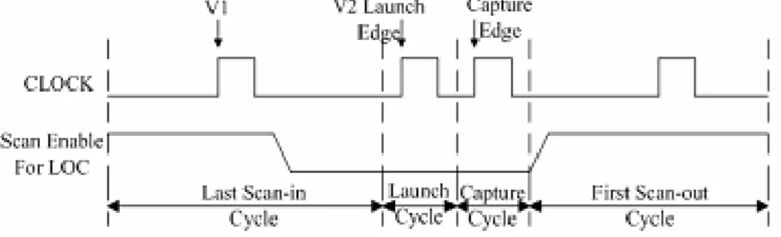
2.3.1 Launch on Capture ... 25
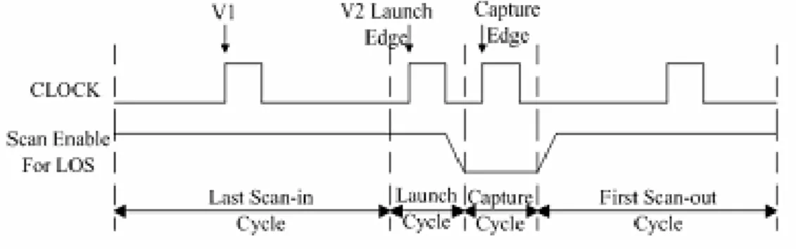
2.3.2 Launch on Shift ... 27
3. Aging Effects in CMOS Nano Technologies ... 29
3.1 Negative Bias Temperature Instability ... 30
3.2 Time Dependent Dielectric Breakdown ... 31
3.3 Hot Carrier Injection ... 33
3.4 Electromigration ... 34
3.5 Stress Induced Voids ... 36
3.6 Total Ionizing Dose ... 37
4. BIST for Delay-Faults ... 41
4.1 Scan Based BIST for Delay-Faults ... 42
4.1.1 Mux Block ... 43
4.1.2 LFSR PI Block ... 44
4.1.4 LFSR Scan Counter ... 49 4.1.5 MISR Block ... 51 4.1.6 Comparators... 52 4.1.7 CUT ... 54 4.1.8 BIST Controller ... 55 4.2 BISTGen Software ... 61 4.2.1 Data Entry ... 61 4.2.2 Application Flowchart ... 62
4.2.3 Database Architecture and Composition ... 63
4.2.4 LFSR’s Configuration ... 64
4.2.5 Application Forms Function and Hierarchy ... 69
5. Aging Sensor Methodology ... 73
5.1 Background and Previous Work ... 73
5.2 Aging Sensor Methodology For Scan-Based BIST Circuits ... 75
5.3 Aging Analysis and Circuit’s Degradation with Aging... 77
6. Results ... 79
6.1 Simulation Environment and Test Procedures ... 79
6.1.1 VHDL Simulation Procedure ... 79
6.1.2 Verilog, AgingCalc, and SPICE Simulation Procedure ... 80
6.2 Results for BIST Circuitry and BISTGen Tool ... 81
6.2.1 CUT_example Circuit... 82
6.2.2 B01, B06 and Pipeline Multiplier Circuits ... 91
6.3 Results for the Aging Sensor Methodology ... 92
6.3.1 CUT_example Circuit... 92
6.3.2 B01 Circuit Simulation Results ... 93
6.3.3 B06 Circuit Simulation Results ... 94
7. Conclusions and Future Work ... 97
7.1 Conclusions ... 97
7.1.1 Conclusions on Scan-Based BIST and BISTGen Tool ... 97
7.1.2 Conclusions on Aging Sensor Methodology ... 99
7.2 Future Work ... 100
xvii
L
IST OFF
IGURESFigure 1: Test Cost vs Manufacturing Cost (From Semiconductor Industry
Association [2]) ... 2
Figure 2: A Scan design schematic. ... 11
Figure 3: Basic BIST Architecture ... 13
Figure 4: Linear LFSR External ... 15
Figure 5: Modular LFSR Internal ... 17
Figure 6: Modular LFSR as Response Compacter ... 20
Figure 7: Linear Multiple Input Signature Register ... 22
Figure 8: Modular Multiple Input Signature Register ... 23
Figure 9: Modular Multiple Input Signature Register with 3 bit Input Pattern ... 24
Figure 10: Launch on Capture ... 26
Figure 11: Launch on Shift ... 28
Figure 12: Relationship between TDDB and Leakage Current [49]. ... 32
Figure 13: Relationship between TDDB and the Electric Field [49]. ... 32
Figure 14: Substract and Gate Currents in a NMOSFET at Low VG ... 33
Figure 15: Substract and Gate Currents in a NMOSFET at High VG ... 34
Figure 16: Schematic Representation of the Damage Induced by Radiation in a MOS Structure [64]. ... 38
Figure 17 : Parent BIST Block Structure ... 43
Figure 18: Switch Multi MUX ... 43
Figure 19: LFSR PI ... 45
Figure 20: LFSR Scan ... 47
Figure 21: LFSR Scan Counter ... 49
Figure 22: MISR Block Diagram ... 51
Figure 23: Comparator Block ... 52
Figure 24: Insertion of a Scan Chain into a CUT ... 54
Figure 25: BIST Specific State Machine ... 56
Figure 26: BIST Controller Block Diagram ... 57
Figure 28: Database Components Architecture ... 64
Figure 29: Comparator block for LFSR PI Patterns ... 66
Figure 30 : LFSR Stop Limit and Rotation ... 67
Figure 31: Global File Structure ... 69
Figure 32: Set of signatures of the XTRAN circuit for two different samples (Monte Carlo analysis), as a function of VDD (1.8 ; 3.3) V [76]. ... 74
Figure 33: Top diagram of the multi-VDD self-test scheme. ... 75
Figure 34: VHDL Simulation Steps ... 80
Figure 35: Verilog, AgingCalc and HSpice simulation steps. ... 80
Figure 36: CUT_example circuit schematic. ... 82
Figure 37: VHDL CUT Signature through ModelSim ... 90
Figure 38: Verilog CUT Signature through HSpice (CosmosScope) ... 90
Figure 39: CUT_example’s BIST signatures for VDD and aging variations (VSC evolution with aging). ... 93
Figure 40: B01’s BIST signatures for VDD and aging variations (VSC evolution with aging). ... 94
Figure 41: B06’s BIST signatures for VDD and aging variations (VSC evolution with aging). ... 95
xix
L
IST OFT
ABLESTable 1: Linear LFSR System of Equations ... 15
Table 2: Modular LFSR System of Equations ... 17
Table 3: Five bits Modular LFSR Circuit Response ... 20
Table 4: LFSR Polynomial Division Result ... 21
Table 5: Linear MISR System of Equations ... 23
Table 6: Modular MISR System of Equations ... 24
Table 7: Modular MISR System of Equations with 3 Input bits ... 24
Table 8: Mux code slice in Verilog ... 44
Table 9: Mux code slice in VHDL ... 44
Table 10: LFSR PI Linear and Modular code slice in Verilog ... 46
Table 11: LFSR PI Linear and Modular code slice in VHDL... 46
Table 12: LFSR Scan Linear and Modular code slice in Verilog ... 48
Table 13: LFSR Scan Linear and Modular code slice in VHDL ... 48
Table 14: LFSR Scan Counter Linear and Modular code slice in Verilog ... 50
Table 15: LFSR Scan Counter Linear and Modular code slice in VHDL ... 50
Table 16: MISR Linear code slice in Verilog ... 51
Table 17: MISR Linear code slice in VHDL ... 52
Table 18: LFSR Comparators code slice in Verilog ... 53
Table 19: LFSR Comparators code slice in VHDL ... 53
Table 20: VHDL CUT before and after Scan insertion... 55
Table 21: Verilog Controller code in Launch-on-Shift ... 58
Table 22: VHDL Controller code in Lunch-on-Shift ... 61
Table 23: Linear type Verilog LFSR PI File ... 65
Table 24: Comparator Block Code for LFSR PI Patterns ... 67
Table 25: LFSR Scan Counter Stop Counting Process ... 68
Table 26: VHDL vs Verilog Entity ... 70
Table 27: Inputs and Outputs different Names ... 71
Table 28: Generic CUT Hardware Description either VHDL or Verilog ... 83
Table 30: Main module from VHDL LOS based BIST Aggregate File ... 85 Table 31: Verilog LOS based BIST File ... 89 Table 32: Config features for Verilog BIST B01 File ... 91 Table 33: Config features for Verilog BIST B06 File ... 91 Table 34: Config features for Verilog BIST Pipeline Multiplier 4-2 File ... 91
xxi
A
CRONYMSASIC Application Specific Integrated Circuit
ATE Automatic Test Equipment
BIST Built-In Self-Test
CAD Computer Aided Design
CHC Channel Hot Carrier
CRC Cyclic Redundancy Check
CUT Circuit Under Test
DFT Design for Testability
DVS Dynamic Voltage Scaling
EDA Electronic Design Automation
FSM Finite State Machine
HDL Hardware Description Language
HTOL High Temperature Operating Life
ICs Integrated Circuits
JTAG Joint Test Action Group
LFSR Linear Feedback Shift Register
MISR Multiple Input Signature Register
NBTI Negative Bias Temperature Instability
ORA Output Response Analysis
RM Response Monitor
RTL Register Transfer Level
SIV Stress Induced Voiding
SoC System on Chip
SRAM Static Random Access Memory
STF Slow to Fall
STR Slow to Rise
TDDB Time Dependent Dielectric Breakdown
TF Transition Fault
VHDL Very high speed integrated circuits (VHSIC) Hardware Description Language
VHSIC Very High Speed Integrated Circuits
VLSI Very Large Scale Integration
xxiii
L
IST OFD
EFINITIONS[Aliasing] – During circuit response compaction, because of the information loss, it is
possible that a signature of a bad circuit may match the good circuit signature, which is called aliasing. In such cases, a failing circuit will pass the testing process.
[Compaction] – A method of drastically reducing the number of bits in the original
circuit response during testing in which some information is lost.
[Compression] – A method of reducing the number of bits in the original circuit
response during testing in which no information is lost, so the original output sequence can be fully regenerated from the compressed sequence.
[Delay Fault] – A delay-fault is a fault that causes the combinational delay of a circuit
to exceed the clock period.
[Negative Bias Temperature Instability] – Translate an increase in the absolute threshold
voltage causing a degradation of the mobility, drain current and transconductance of P-channel MOSFETs. It is almost universally attributed to the creation of interface traps and oxide charge by a negative gate bias at elevated temperature.
[Path Delay Fault] – A delay defect in a circuit is assumed to cause the cumulative
delay of a combinational path to exceed some specified duration. The combinational path begins at a primary input or a clocked flip-flop, contains a connected chain of gates, and ends at a primary output or a clocked flip-flop. The specified time duration can be the duration of the clock period (or phase), or the vector period. The propagation delay is the time that a signal event (transition) takes to traverse the path. Both switching delays of devices and transport delays of interconnects on the path, contribute to the propagation delay.
[Signature] – A statistical property of a circuit, usually a number computed for a circuit
from its responses during testing, with the property that faults in the circuit usually cause the signature to deviate from the signature of the non-faulty circuit.
[Signature Analysis] – A method of circuit response compaction during testing, whereby
the entire good circuit response is compacted into a good circuit signature. The actual circuit signature is generated during the testing process on the CUT, and then compared with the good machine signature to determine whether the CUT is faulty.
[Transition Delay Fault Model] – “It is assumed that in the fault-free circuit all gates
have some nominal delay and the delay of a single gate has changed. The gate-delay, usually an increase over the nominal value, is assumed to be large enough to prevent a passing transition from reaching any output within the clock period, even when the transition propagates through the shortest path. Possible transition faults of a gate are slow to-rise and slow-to-fall types and hence the total number of transition faults is twice the number of gates. Transition faults model spot defects and are also called gross-delay-faults” (excerpted from [27]).
1
1. I
NTRODUCTIONElectronic systems have increased its complexity in the last years in nano technologies, which leads to a growth of system functionalities integrated in a single chip. High performance applications with Integrated Circuits (IC) are commonly found in the networking, banking, aerospace/defence, automotive, computer, telecommunications and healthcare industries, and have greatly increased in usability and complexity. Such, evolution requires additional fault control in the test environment, as testing of IC has a crucial importance to ensure a high level of quality in product functionality. Due to the increased complexity in modern ICs, the impact of testing affects both IC design and manufacturing. Moreover, given this range of design involvement, a major concern is, definitely, how to achieve a high level of confidence in IC operation and this desire to attain high quality levels, conflicts with the demand for reduced costs and shorten time involved in the development process. These two design considerations are at constant odds.
The traditional solution to achieve a high level of confidence is ruled by advanced testers denominated Automated Test Equipment (ATE). Traditionally ATE’s cost is only measured using a simple digital cost pin approach which leads to a lack of considerations making the cost per-test in many ways disproportionate. In the last years other calculations have been made and proposed [1] to improve the traditional test cost measurement, considering also base system costs associated with equipment infrastructure, central instruments and the beneficial scaling that occurs with increasing pin count. As an example, Figure 1 shows the test cost evolution vs. manufacturing cost in the last 30 years.
Therefore, it became essential to find/implement alternative test methods to reduce financial costs. Among these methods is Built-In Self-Test (BIST), and has become a major design consideration in Design for Testability (DFT) methods. BIST has many advantages. This technique can drastically reduce the external test equipment dependency. If external test equipment is a part of the enterprise legacy, BIST will reduce the global cost and test time even more, making possible to re-direct the test equipment towards other devices in the current design, if necessary.
Figure 1: Test Cost vs Manufacturing Cost (From Semiconductor Industry Association [2])
Moreover, new technology products need high speed testers, not always available, as ATE is usually a few years behind the latest technology products. Considering that testing represents a key cost factor in the production process (up to 70% of total product cost is reported in [3] [4] [5]), an optimal test strategy can be a substantial competitive advantage in a market comprising billions of electronic components and systems. It is therefore not a surprise that the International Technology Roadmap for Semiconductors (ITRS), in its last report (2012) has placed the design for self-test on the future opportunities in the “Test and Test Equipment” group report [6].
Another important advantage is that BIST allows not only circuit tests during production, but also to test the circuits during their entire lifetime, which is an important feature when long-term degradation effects start to limit circuits expected life-cycle for nanotechnology ICs. This opens a new concept and a new era in system quality and testing. In addition, BIST can overcome pin limitations due to packaging, make efficient use of available extra chip area, and provide more detailed information about the faults present.
The main disadvantages for BIST usability are, commonly, the increased die size and design complexity. However, the addition of BIST features to IC design nowadays doesn't significantly increase a product's size, cost, and production time, as was the case in the past. All the benefits are plentiful motivations for BIST technique to become an important DFT technique in the future.
The present work deals with the automatic generation of BIST structures and studies its behaviour during circuit’s expected lifetime, using statistical predictions for aging degradations. The accelerated aging effects observed in new technologies ICs are also a motivation to develop new techniques to enhance circuit’s reliability. In fact, aging effects caused by phenomena like Negative Bias Temperature Instability
(NBTI) (the dominant long-term effect in nanometer CMOS technologies [72]), Hot Carrier Injection (HCI), or Time Dependent Dielectric Breakdown (TDDB), among others, are gaining increase relevance in new nanometer technologies and degrade circuit performance over time [73]. These aging effects are cumulative and cause circuit’s safety margins (time slack) to be shrinked, reducing the expected circuit’s life time. Therefore, new technology products have a smaller expected lifetime than previous technology’s products, imposing the need for auto-test during on-field operation (and not only in the production stage), along circuit’s lifecycle.
1.1 O
BJECTIVESWith the previous motivations in mind, this work tries to put a milestone in the development of ICs with BIST capability. The goal is to develop automatic BIST structures for generic sequential ICs, aiming the detection of delay-faults, and re-use on-chip variable power supply voltage source to implement an aging aware test strategy to detect long-term degradations during circuit’s lifetime.
The objectives for this work are, mainly, twofold:
1. Implement a software tool to generate BIST structures automatically in a circuit under test (CUT), aiming the detection of delay-faults;
2. Show that a set of auto-tests using a variable VDD power-supply voltage source
(a set of BIST runs, each run using a different power-supply voltage value) can be used as an aging and performance sensor for long-term degradations (during circuits’ lifespan).
The first main objective is a pre-requisite to the second one. It is important to have a tool to insert in a general sequential CMOS circuit BIST structures to allow the auto-test of the circuit. Starting from a HDL (Hardware Description Language) netlist (or behavioural description), the tool must generate automatically a new HDL netlists (or behavioural description) of the new circuit with BIST structures and functionality. To accomplish this first objective, the BIST structures have to be defined, using VHDL (Very high speed integrated circuits Hardware Description Language) and
Verilog languages, and defining the structures in a behavioural and netlist representation, using a CMOS generic standard cell library designed in a previous M.Sc. thesis in ISE-UAlg). The BIST controller defined should also implement LOS and LOC based BIST approaches, aiming the detection of delay-faults.
The second main objective will use as a test vehicle the BIST structures defined with the proposed software tool (from the first objective), already inserted in a Circuit Under Test (CUT), and the purpose is to show by simulation (SPICE simulations) that using by reusing a variable power-supply already present in the IC, it is possible to identified a set of BIST signatures (known as Voltage Signatures Collection, VSC), from a set of BIST sessions performed each one at a different power-supply voltage. This VSC is unique for each sample circuit, and as aging degradations start to occur during circuit’s lifetime, this unique VSC will differ, allowing to detect not only gross delay-faults but also to define an aging sensor methodology for BIST circuits.
1.2 C
ONTEXTThis research work was conducted at the Instituto Superior de Engenharia (ISE), University of Algarve (UAlg), in close collaboration with INESC-ID Lisbon and with the industrial partner Silicongate in Lisbon. The work team formed in the Portuguese institutions are working in collaboration with other foreigner R&D institutes and universities, namely University of Vigo in Spain, the INAOE institute in Mexico and
PUCRS University in Brazil. The team has been developing in the last 5 years some
research work on aging sensors, both for ASIC (Application Specific Integrated Circuit) and for emulated circuits in FPGAs (Field-Programmable Gate Array). Moreover, in this context, 2 M.Sc. thesis were already finished, and another one is currently being developed, in ISE-UAlg, and furthermore M.Sc. and Ph.D. thesis were finished and are currently being developed in partner institutions.
1.3 O
UTLINEThis thesis is organized as follows:
Chapter 2 reviews basic concepts on Fault Modelling, conventional
BIST methodology and its architecture. Emphasis is placed on scan design for delay-fault detection, namely Launch on Capture and Launch on Shift techniques.
Chapter 3 outlines the main phenomena and effects that contribute to the
aging of digital CMOS integrated circuits like NBTI phenomenon.
The fourth chapter describes the new proposed dynamic BIST
methodology. It gives the details about the new methodology, the proposed BIST architecture and the characteristics of all their structural components.
Chapter 5 explains the BISTGen Application Software, its composition
and hierarchy levels.
Chapter 6 presents the test results.
Chapter 7 concludes the work with a summary of the proposed
methodology, its achievements and limitations. It also outlines directions for future work.
7
2. D
ESIGN FORT
ESTABILITYThe design of a feasible system solution for a given problem is only half of the task. Considering that the production stage in the IC design process involves very complex procedures, it is very important to be able to test the system to a degree which ensures a high confidence level that it is fully functional and this is generally not a straight forward task. In very small digital systems scale, it is possible to test it exhaustively, and the system can exercise over its full range of operating conditions. However, in a larger scale system, it is no longer possible to do this procedure and therefore other strategies has to be found to ensure that the system will properly be tested.
When testing a digital logic device, stimulus are applied to its inputs and check its response at the outputs to identify if it is performing correctly. The set of input stimulus is referred as a test pattern. In general, the response of the device is observed at its normal output pins. However, it is possible that the device is specially configured during the test, to allow observing some internal nodes, which generally would not be accessible to the user. The response of the device is evaluated by comparing it to an expected response, which may be obtained by saving the response of a known good device, or using simulation on a computer. If the CUT passes the test, isn’t possible to say categorically that it is a good device. The only possible conclusion is that the device does not contain any of the faults for which it was tested. It is important to grasp this point; a device may contain a huge number of potential faults, some of which may even mask each other under specified operating conditions. The designer can only be sure that the device is 100% good if it has been 100% tested, this is rarely possible in real life systems.
2.1 D
ELAYF
AULTSPhysical failures and fabrication defects cannot be easily modeled mathematically. As a result, these failures and defects are modeled as logical faults.
interconnections among components of a design. Functional faults relate to a functional model, for example an RTL/HDL (Register Transfer Level / Hardware Description Language) model, and these affect the nature of components operation in a design. Testing for functional faults validates the correct operation of a system, while testing of structural faults targets manufacturing defects.
The faults can be static, if represent a defect that is always present and is independent of circuit operation and performance, and dynamic, if the fault only manifests itself in pre-determined circuit operating conditions and, therefore, it is not always present. Delay faults are dynamic faults related with the delay of paths. In other words, if a given timing response is not met, due to a dynamic defect or even due to an excessive clock frequency operation, an error is captured by a memory cell (usually a flip-flop or latch), and is conclusive that a delay-fault occurred.
Two popular structural fault models are prevalent in the industries today which are the stuck-at fault model and the transition fault model. Stuck-at faults affect the logical behaviour of the system and are a representation of static faults. However, transition faults affect the timing/temporal behaviour of the system and are a representation of dynamic faults. An additional fault model being used is the path
delay-fault model, which is also based on the timing behaviour of the system, but
cumulative delays along paths are considered, instead of delays at each net as in the transition fault model. This previous fault model is also a representation of dynamic faults. Therefore, transition and path delay-fault models are commonly mention as two delay-fault models.
2.1.1 TRANSITION FAULTS
The transition fault model is similar to the stuck-at fault model in many ways. The effect of a transition fault at any P point in a circuit is that any transition at P will not reach a scan flip-flop or a primary output within the stipulated clock period of the circuit. According to the transition fault model [28], there are two types of possible faults on all lines (nodes) in the circuit: a slow-to-rise fault (STR) and a slow-to-fall fault (STF). A slow-to rise fault at a node means that any transition from ‘0’ to ‘1’ on the node does not produce the correct result when the device is operating at its
maximum operating frequency. Similarly, a slow-to fall fault means that a transition from ‘1’ to ‘0’ on a node does not produce the correct result at full operating frequency. In any circuit, the time slack can be defined as the difference between the clock period and the propagation delay of the path under consideration (i.e. the remaining and unused time of the clock period, in signal propagation). For a gate level delay-fault to cause an incorrect value to be latched at a circuit output, the size of the delay-fault must be such that it exceeds the slack of at least one path from the site of the fault to the site of an output pin or flip-flop. If the propagation delays of all paths passing through the fault site exceed the clock period, such a fault is referred to as a gross delay-fault [29].
Any test pattern that successfully detects a transition fault comprises of a pair of vectors {V1, V2}, where V1 is the initial vector that sets a target node to the initial value, and V2 is the next vector that not only launches the transition at the corresponding node, but also propagates the effect of the transition to a primary output or a scan flip-flop [30]. In other words, a set of test vectors that test for a delay-fault at the output or input of a gate are such that:
A desired transition is launched at the site of the fault
If the fault is a slow-to rise fault, the final pattern is a test for a corresponding stuck-at-0 fault, and if the fault is a slow-to fall fault, the final pattern is a test for a corresponding stuck-at-1 fault.
When compared with tests for stuck-at faults, it can be seen that the only additional requirement to test for transition faults is the presence of a pattern that initializes a node to the required value, just before the application of a stuck-at fault pattern. One might expect that the fault coverage attained by testing transition fault patterns will be close to that attained by testing stuck-at fault patterns. However, should be remembered that the fault coverage obtained for transition fault patterns represent only gross delay-faults. More detailed analysis will be necessary to evaluate for smaller delay-faults [31].
2.1.2 PATH DELAY FAULTS
The path delay-fault model [34] takes the sum of all delays along a path into effect, while the transition fault model accounts for localized faults (delays) at the inputs and outputs of each gate. There may be cases where the gate delays of individual faults are within specified limits, but the cumulative effect of all faults on a path may cause an incorrect value to be latched at the primary outputs, if the total delay exceeds the functional clock period. The transition fault model cannot account for such defects, but the path delay-fault model can. However, in a design containing
n lines, there can be a maximum on 2n transition faults (a slow-to rise and slow-to
fall fault on each line), but there can potentially be 2n path delay-faults (considering
all possible paths) [29]. Since all the paths cannot be tested, the path delay model requires identification and analysis of critical paths in the design. This makes it more complicated to use on large designs and hence, the transition fault model has been accepted as a good method to test for delay-faults in the industry [35] [36].
2.2 D
FT
T
ECHNIQUES FORS
TATICF
AULTSDfT techniques have been used in digital ICs to achieve, fault detection, test circuit insertion, fault coverage analysis and test pattern generation, among other things related to test. Digital circuits are usually tested using the stuck-at fault model, which considers all faults in a digital IC as either tied up to logic ‘1’ or down to logic ‘0’. All digital faults can be categorized into either stuck-at-0 or stuck-at-1 faults and can assume that every node can have either one of these two possible faults. For any given combinational circuit, a truth-table can be generated by simulation of all possible inputs. For a certain single-fault existing in the circuit-under-test (CUT), it is called a detectable fault if a different truth table is generated by the simulation of all possible inputs. For a test sequence, the ratio of detectable faults to all possible faults of a digital circuit is called fault coverage. The input values that can detect at least one fault are considered test patterns. Thus, test patterns are generated to detect faults in a digital device and the testability of the given device can be measured by fault
coverage. A path sensitization technique [7] is used to find proper test patterns for any given detectable fault. Finally, fault collapsing techniques [8] are used to remove many stuck-at faults and to reduce the total number of test patterns. Over the years, two major methods have been widely adopted by integrated circuit (IC) industry to address the digital testing issues: Scan Path and BIST.
2.2.1 SCAN PATH
Since the inception of IC design in the mid-1960s, IC test has been an integral part of the manufacturing process. Initially, tests were either randomly generated or created from verification suites. But as chips got larger, this process required a more targeted approach, one that needed to be easily replicated from one design to another. This led to the invention of scan, which made designs combinational and simplified the test generation process.
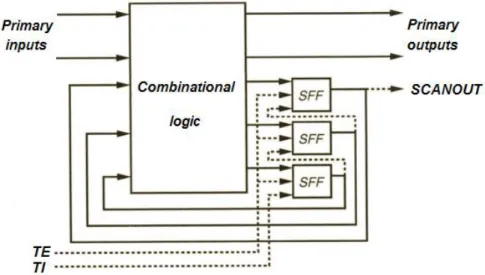
Scan path is a method to set and observe every flip-flop inside a digital IC chip by replacing all regular flip-flops (FF) with scan FFs and two additional input pins, test enable (TE) and test input (TI). All SFFs are in a chain which is connected through TI pin and SCANOUT pin, as shown in Figure 2.
Figure 2: A Scan design schematic.
When TE pin is enabled which means shift mode, the scan chain can be accessed by standard JTAG I/O [9] pins to read and set all SFFs. After all SFFs are
settled into a desired state, TE pin is disabled (capture mode) and output of combinational logic can be captured in SFFs. Then TE pin is enabled again to shift out the Q pin of SFFs, bit by bit through the scan chain to SCANOUT, and at the same time, a new pattern is shifted in to set all SFFs to the next desired state (through TI). Scan chain makes it possible to assign an arbitrary internal state to a digital IC and thus may achieve higher test coverage with fewer test patterns.
In the modern System-on-Chip (SoC) design, many cores are integrated into a single chip. Some of them are embedded, and cannot be accessed directly from the outside of the chip. Such SoC designs make the test of these embedded cores become a great challenge.
2.2.2 BIST
BIST is one of most popular test solutions to test embedded cores [10]. As the digital circuit technology is moving to high densities of integration, BIST has become
a primary issue in the realm of VLSI (Very Large Scale Integration) circuit design.
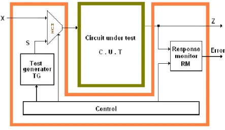
Techniques for design for testability and BIST consider the testing problem during the design stage of digital devices and have been found to be extremely effective. The central idea behind BIST is to have the chip to test itself. This technique generates test patterns and evaluates output responses inside the chip [11] [12] [13]. Built-in Self-test is gaining popularity as a means to address Self-test issues at the different packaging levels of digital systems. One of the benefits of BIST is the fact that no patterns need to be stored in the test equipment, which is simply required to provide a clock and a few control signals. This is especially important when high performance systems are being tested. BIST also makes the chip/board/system more independent of the specific test resources available at each manufacturing stage. BIST is also a convenient way of applying more test patterns, to compensate for the weaknesses of the stuck-at fault model [14]. BIST can significantly improve the testability of VLSI chips and save testing time as well [15]. BIST is a DFT technique that places the testing functions physically with the CUT, as illustrated in the Figure 3.
Figure 3: Basic BIST Architecture
In normal operating mode, the CUT receives its inputs X from other modules and performs the function for which it was designed. In test mode a test generator (TG) through a Linear Feedback Shift Register (LFSR) applies a sequence of test patterns to the CUT, and the response monitor (RM or Output Register Analyser (ORA)) using a multiple input signature register (MISR) for the effect compact test responses received from primary output. The response signatures are compared with reference signatures generated or stored on-chip, and the error signal indicates any discrepancies detected. The basic blocks that forms the BIST are: TG (LFSR), CUT, RM (SISR/MISR, Single/Multiple Input Signature Register), BIST controller and signature analyzer. BIST techniques make testing of a digital IC chip easier, faster, more efficient and less costly. At the cost of approximate by 20% – 30% overhead in the chip area and a small penalty in performance due to additional BIST hardware [16], the IC chip can now perform testing through internal scan chains without an external automatic testing equipment (ATE).
2.2.2.1 TEST PATTERN GENERATION
BIST is a DFT technique which allows the circuit to test itself without any external equipment [23]. BIST implementation requires primarily two components: a pseudo-random test pattern generator (for test vector generation) and a data compactor (for output response analysis) [24]. There are several types of test patterns that can be used
in BIST: deterministic, algorithmic, exhaustive, pseudo-exhaustive, or even random. However, due to hardware costs, the most commonly used are the pseudo-random test patterns. These components are mostly implemented using LFSRs and Cellular Automata (CA).
LFSR is constructed using flip-flops connected as a shift register with feedback paths that are linearly related using XOR gates. An LFSR can be used for generation of pseudo-random patterns, polynomial division, and response compaction. The CA is very similar to the LFSRs except that the registers in CA have a logical relationship with their neighbours only. This leads more randomness in the pattern generated. LFSR is more popular for implementation of both TPG and ORA due to its compact and simple structure. However, CA is gaining popularity in many cases because of their characteristics and ease of modification.
Linear Feedback Shift Register or LFSR is a shift register whose output is the result of XOR of some of its inputs [22]. There are two ways to implement LFSRs: internal feedback and external feedback. These techniques differ in the way feedback is applied. All the flip-flops that feed a XOR gate are known as taps. These taps decide the pattern generated by the LFSR and hence define the characteristic polynomial of an LFSR, where n is the degree of the polynomial which is defined by
the number of bits/nodes of the LFSR. Notice that the terms ‘x ’ and ‘0 xn1’ are
always present and the remaining terms indicate the location of the taps in the circuit. The degree of the polynomial n is equal to the number of bits in an n-bit LFSR pattern. An all zeroes state is invalid for an LFSR with XOR gates (the same for all ‘1’ bits for an LFSR with XNOR gates), as the state would never change if all the bits are ‘0’ or ’1’. Therefore, the maximum number of unique patterns an n-bit LFSR can
generate is2n 1, where n is the number of bits. Special LFSRs can be constructed to
generate the all zeroes (ones) state also, but they have a larger area overhead associated with them, as described in [25]. In case of an external feedback LFSR, the XOR gates are in the feedback path and the input to the shift register is the XOR of all the taps.
Figure 4: Linear LFSR External
But let’s take a close look with a mathematical model support and start with the
standard type (Linear LFSR or external). In the Figure 4 each tap of the coefficient C i
indicates the presence or absence of feedback from that particular flip-flop position into flip-flop positionXn1. This is indicated by setting Ci(0in1)to ‘1’ if the
feedback exists, and to ‘0’ if there is no feedback in that particular position. In the
actual hardware, if C is ‘0’, then there is no XOR gate in the feedback network for i
that bit position; otherwise, the XOR gate is included. Multiplication by x is
equivalent to a right shift in the LFSR register by one bit, and the addition operation is
the XOR () operator. Therefore, addition is equivalent to XOR subtraction,
so000,011,101,110. This is because there are no carries or borrows
in XORing arithmetic. The following matrix describes the system of equations:
) ( ) ( ) ( ) ( ) ( C -C C C 1 1 0 0 0 0 0 1 0 0 0 0 0 1 0 0 0 0 0 1 0 ) 1 ( ) 1 ( ) 1 ( ) 1 ( ) 1 ( 1 2 3 1 0 1 -n 2 -n 2 1 1 2 3 1 0 t X t X t X t X t X t X t X t X t X t X n n n n n n
Table 1: Linear LFSR System of Equations
This system is written as:
X(t1)TsX(t )
The first column of Ts is ‘0’, except for the last row, to indicate that the flip-flops shift
to indicate that X receives input from0 X , and so one. Finally, the 1 th
n element in the
first column is ‘1’ to indicate that X always feeds back into 0 Xn1 through the XOR
feedback network. The remaining elements in the nth row are the feedback
coefficientsC , which indicate whether the remaining flip-flops feed back into i Xn1
or not. We also see why this LFSR cannot be initialized to all zeros. If that were done, the feedback network and the right shifts of the flip-flops would always produce all zeros, and the LFSR would hang in the all-zero state. Note that the + operator implied
in this matrix system is actually the XOR () operator. If X is the LFSR initial state,
the LFSR will progress through the states: X,TsX,Ts2X,Ts3X,.... The matrix period
is the smallest integer k such that:
I Tsk
Where I is the identity matrix, k is the LFSR cycle length (k = 0 for X = 0), and Tsis
known as the companion matrix. Recall that multiplication by x is equivalent to
shifting a bit through the D flip-flop register of this LFSR. Therefore, we view X as 0
the constant 1 and X1 x.X0 x, X2 x.X1x2, ... ,Xn x.Xn1 xn .This hardware system can be described by the characteristic polynomial:
n i i i n n n n n s I X c x c x c x c x x c x T x P 0 1 1 2 2 2 2 1 ... 1 . ) (The modular, internal exclusive-OR, or Type 2 LFSR is described by a companion
matrixTM TST, which is the transpose of TS. It is called an internal XOR LFSR
because the feedback XOR gates are located between adjacent flip-flops. The modular LFSR can run somewhat faster than the standard LFSR because it has at most one XOR gate delay between adjacent flip-flops. However, this is not a serious consideration in testing because actual circuits always have more logic gates between flip-flops than there are XOR gates in the feedback network of the external XOR LFSR. Moreover, for practical tests the test patterns generated by LFSRs are not more than 22-25 bits wide, so bigger circuits are partitioned into small sub-circuits of
less than 25 primary inputs [26]. The Figure 5 shows the modular LFSR circuit implementation.
Figure 5: Modular LFSR Internal
The mathematical respective system of equations is presented in the next matrix.
) ( ) ( ) ( ) ( ) ( ) ( C 1 0 0 0 0 C 0 1 0 0 0 C 0 0 0 0 0 C 0 0 0 1 0 C 0 0 0 0 1 1 0 0 0 0 0 ) 1 ( ) 1 ( ) 1 ( ) 1 ( ) 1 ( ) 1 ( 1 2 3 2 1 0 1 -n 2 -n 3 -n 2 1 1 2 3 2 1 0 t X t X t X t X t X t X t X t X t X t X t X t X n n n n n n
Table 2: Modular LFSR System of Equations
This system is written as:
X(t) )
1
(t TM
X
This hardware system can be described by the characteristic polynomial:
n i i i n n n n n M I X c x c x c x c x x c x T x P 0 1 1 2 2 2 2 1 ... 1 . ) (In the LFSR of the Figure 5, a right shift is equivalent to multiplying the register
contents by , and then dividing its value by the characteristic polynomial and storing x
Every LFSR can be realized either in standard or modular form. Both use m XOR
(or XNOR) gates, where m is the number of non-zero C feedback coefficients in the i
LFSR.
2.2.2.2 OUTPUT RESPONSE ANALYSIS
During BIST, it is necessary to reduce the enormous number of circuit responses to a manageable size that can be stored on the chip. For example, consider a circuit with a hardware pattern generator that computes 5 million test patterns during testing, and
where there are 300 P OS. The total number of resulting responses will be:
000 000 500 1 300 000 000 5 bits!
This huge amount of information cannot be economically stored, so the circuit responses must be compacted.
In this matter, we must distinguish between compression and compaction. Circuit
response compression is lossless, because the original output sequence (1.5109bits
in the previous example) can be completely regenerated from the compressed sequence. Compaction, however, results in information loss, so regenerating the original circuit response information is not possible. Compression schemes, at present, are impractical for BIST response analysis, because they inadequately reduce the huge volume of data, so only compaction schemes are used. In mathematical words, compression functions are invertible, but compaction functions are not.
Signature analysis is the process of compact the circuit responses into a very small bit length number, representing a statistical circuit property, for economical on-chip comparison of the behaviour of a possibly defective chip with a good one. Frohwerk [81] invented signature analysis in 1977 at Hewlett-Packard. Also, the signature must preserve as much as possible of the fault information contained in the circuit output response before compaction, and the circuitry used to implement the compacter should be small [31]. All compaction techniques require that the fault-free circuit signature be known.
Some schemes for response compaction are; (i) Parity checking, where parity is formed across all circuit responses; (ii) Ones counting, where the number of ones is counted in the output responses from the circuit. Savir [82] pioneered syndrome testing, in which pattern generation must be exhaustive, and ones counting is used for response compaction.
Aliasing occurs when the compacted response of the bad circuit matches the compacted response of the good circuit, and there is always a problem with compaction because information is lost. In parity checking, aliasing frequently happens. Also, with ones counting, it is possible to permute the placement of ones in the circuit’s Karnaugh map, and still obtain a correct ones count, so it is also very prone to aliasing and also requires significant arithmetic hardware.
Hayes [83] described transition count testing. The transition count, C(R), is the number of times signals in the circuit response R change during BIST. Transition count test aliases less than ones counting, because it not only checks for the correct number of ones and zeros in the circuit output response, but also partially test for the correct ordering of the ones and zeros in the response.
2.2.2.2.1 LFSR FOR RESPONSE COMPACTION
Frohwerk [81] introduced the LFSR for response compaction by signature analysis. The signature is any statistical property of the circuit that is used for checking its correct operation. He used the data compaction method of the Cyclic Redundancy Check (CRC) code generator, which requires an LFSR hardware device. In this method, the circuit output data stream is treated as a descending order coefficient polynomial. The output response compacter LFSR performs polynomial division of this data stream polynomial by the characteristic polynomial of the LFSR. The Figure 6 shows a specific modular LFSR as a response compacter. The Table 3 presents the response of the circuit as the bits (01010001) are shifted into the LFSR through the XOR gate and the respective mathematical support for remainder generation.
Figure 6: Modular LFSR as Response Compacter Inputs X0 X1 X2 X3 X4 Initial State 0 0 0 0 0 [1º] 1 1 0 0 0 0 [2º] 0 0 1 0 0 0 [3º] 0 0 0 1 0 0 [4º] 0 0 0 0 1 0 [5º] 1 1 0 0 0 1 [6º] 0 1 0 0 1 0 [7º] 1 1 1 0 0 1 [8º] 0 1 0 1 1 0
Table 3: Five bits Modular LFSR Circuit Response
Data stream polynomial = (0 1 0 1 0 0 0 1)
Data stream polynomial = 0.x0 1.x10.x21.x30.x40.x50.x61.x7
Data stream polynomial = x x3 x7
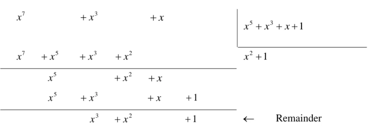
Remainder = (1 0 1 1 0)
Remainder =1.x0 0.x1 1.x2 1.x3 0.x4
![Figure 6: Modular LFSR as Response Compacter Inputs X 0 X 1 X 2 X 3 X 4 Initial State 0 0 0 0 0 [1º] 1 1 0 0 0 0 [2º] 0 0 1 0 0 0 [3º] 0 0 0 1 0 0 [4º] 0 0 0 0 1 0 [5º] 1 1 0 0 0 1 [6º] 0 1 0](https://thumb-eu.123doks.com/thumbv2/123dok_br/18038482.861926/46.892.160.681.136.313/figure-modular-lfsr-response-compacter-inputs-initial-state.webp)

![Figure 16: Schematic Representation of the Damage Induced by Radiation in a MOS Structure [64].](https://thumb-eu.123doks.com/thumbv2/123dok_br/18038482.861926/64.892.254.582.267.477/figure-schematic-representation-damage-induced-radiation-mos-structure.webp)