2017
UNIVERSIDADE DE LISBOA
FACULDADE DE CIÊNCIAS
DEPARTAMENTO DE ENGENHARIA GEOGRÁFICA, GEOFÍSICA E ENERGIA
The role of different crucible materials on silicon ingots
contamination
Gonçalo Rafael Ferreira Dias
Mestrado Integrado em Engenharia da Energia e do Ambiente
Dissertação orientada por:
i
Acknowledgments
The present work is part of a common effort between NTNU, SINTEF, IFE - Institutt For Energiteknikk, REC Solar, REC Silicon, Steuler Solar and The Quartz Corp to understand how impurities can be better controlled in high performance multicrystalline silicon for solar cells, gathering more knowledge about their sources, transport mechanisms and the repercussions in cell performance.
Throughout it, the encouragement and guidance of my supervisor at NTNU, Prof. Marisa di Sabatino, has been fundamental. I deeply appreciate her recommendations and the trust put in me for working and learning in Trondheim, at a prestigious university where I have been well received and supported. I would also like to express my appreciation towards my supervisor at FCUL, Prof. João Serra for his advice and aid on being able to do this dissertation in Norway. Furthermore, I am thankful to Dr. Gaute Stokkan, for his constructive criticism and suggestions, and Dr. Kai Erik Ekstrøm, for his sympathy and time spent when training me on lab equipment. The help from the technical staff of the Department of Materials Science and Engineering and SINTEF has also allowed me to develop skills in sample preparation and heat treatment, making this experience more fruitful and enjoyable.
In addition, I want to mention my friends, colleagues and the good people I have met in Norway for their kindness, opinions and motivation. Lastly, I am extremely grateful to my parents, who have been tireless when providing me with this opportunity.
ii
Resumo
Esta dissertação apresenta uma revisão sobre a influência do material constituinte do cadinho, entre outros componentes, na quantidade de impurezas presente em lingotes de silício multicristalino, obtidos por solidificação direcional. Seguidamente, são apresentadas medidas propostas para a sua mitigação. Na obtenção de lingotes com baixas concentrações de impurezas, parâmetros como o nível de pureza do cadinho e do filme de nitreto de silício são apontados. O filme é tipicamente aplicado nesta prática de para evitar a adesão do lingote ao cadinho. Juntamente, as condições de escoamento do silício em fase líquida e da atmosfera circundante são assinaladas como relevantes.
Também neste trabalho, é desenvolvido um procedimento experimental através de tratamentos térmicos de pares de difusão, realizado na NTNU. O seu objetivo é a caraterização das difusividades de ferro e titânio num cadinho comercial de nitreto de silício. Este é uma alternativa reutilizável que tem vindo a ser proposta aos mais estabelecidos cadinhos de quartzo, que sofrem transições de fase na gama de temperaturas do processo, levando a uma súbita redução de volume que põe em causa a sua integridade. Para além do nitreto de silício permitir o crescimento de vários lingotes, é ainda, tipicamente, melhor condutor de calor. Tais aspetos levam a considerar uma redução dos custos de produção dos lingotes, do ponto de vista do investimento em cadinhos, bem como do gasto energético durante o processo. É, porém, necessário assegurar que as células fotovoltaicas sintetizadas a partir destes lingotes não são afetadas no ponto de vista da sua eficiência de conversão. Face a células de silício monocristalino, tem vindo a ser demonstrado que as perdas em silício multicristalino se devem à presença de defeitos na rede cristalina, que promovem a recombinação dos portadores de carga, principalmente sob a forma de deslocações e impurezas eletricamente ativas, onde se destacam o ferro e outros metais de transição. Por forma a reduzir a sua presença, diversas práticas são aplicadas durante a sintetização de matéria-prima e componentes auxiliares de elevada pureza, no decorrer da recristalização e nas seguintes etapas. No contexto do trabalho experimental, o mecanismo de difusão de impurezas do cadinho para o silício ocorre durante a solidificação direcional. O estudo das difusividades no cadinho, por intermédio de pares de difusão, evita a deposição do filme antiaderente, assim como os gastos relativos à obtenção de lingotes.
Estes são constituídos por uma amostra do cadinho, em contato com outra de silício monocristalino. Os materiais foram facultados pela STEULER SOLAR e o SINTEF, respetivamente. Para se manterem unidos durante o tratamento térmico, os pares são envolvidos com fio de kanthal, numa fase preliminar, permitindo o estudo do titânio, enquanto que para o ferro este fio é substituído por um peso de silício, obtido da porção do lingote de Czochralski, de onde se cortam as referidas amostras.
As espessuras adequadas para as amostras de silício foram estimadas de acordo com a 2ª lei de Fick para temperaturas até 1350 ºC, com base na difusividade e solubilidade dos elementos referidos, descrita em silício por vários autores. Todavia, tal não se verifica para nitreto de silício, para o qual as publicações geralmente abordam filmes, resultantes da deposição química de vapor em substratos de silício, onde atuam como barreiras de difusão. Consequentemente, a sua estrutura cristalográfica difere consideravelmente da cerâmica em análise, levando a por em causa a sua aplicabilidade neste caso de estudo. Além disso, estes coeficientes ainda não foram publicados tanto para ferro, como para titânio. Após o tratamento térmico, os perfis de concentração das impurezas são analisados em corrente contínua através de espetrometria de massa por descarga luminescente (GD-MS), ao longo da espessura das amostras de silício. O mesmo não é feito para o cadinho que, por tratar-se de um isolante elétrico, requer outro método não disponível no decorrer dos trabalhos. Deste modo, com um ajuste à 2ª lei de Fick é
iii
possível estimar quantidade de impureza transportada para a amostra de silício, a partir da qual se obtém indiretamente o coeficiente de difusão na cerâmica. Eventualmente, pode também ser verificado o limite de solubilidade e a difusividade à temperatura do tratamento.
Outro aspeto preponderante para determinar a difusividade no cadinho, é sua composição elementar, principalmente no que toca a ferro e titânio. A análise por espetrometria de massa por plasma acoplado indutivamente (ICP-MS) adequa-se ao limite de deteção exigido, pelo menos na ordem das ppbm. Todavia, a dissolução do nitreto de silício em soluções de ácido nítrico e fluorídrico resulta numa quantidade de sólidos superior à imposta pela técnica. Por esse motivo foi considerada a ficha técnica do fabricante.
Os requisitos para estudos semelhantes com pares de difusão são sublinhados, seguidos de uma melhor descrição do mecanismo de difusão de titânio no cadinho. Os resultados sugerem que o procedimento experimental ainda carece de ajustes por forma a estudar ferro com sucesso, uma vez que há indícios de contaminação por fontes indesejáveis.
A observação das amostras aponta para a presença duma fonte desconhecida, desde o instante anterior ao tratamento térmico. Esta possibilidade surge já que a difusão para as amostras ocorre a uma taxa muito mais rápida com temperaturas elevadas, do que durante o período de arrefecimento. Questionando se os refratários no interior do forno fossem a fonte, a contaminação deveria ser mais percetível nos tratamentos com períodos mais longos, devido à exposição prolongada. No entanto, este não é sempre o caso. Como causas mais prováveis assinalam-se a hipotética presença de partículas com ferro nas superfícies do laboratório, onde se realizam outros tratamentos térmicos. O contato com os pares de difusão ocorreu antes do aquecimento, devido às medidas de segurança impostas pelas elevadas temperaturas, justificando o uso de luvas de proteção e pinça.
Um método de diferenças finitas foi criado para estimar a difusividade de titânio a partir dos perfis de concentração em função da espessura. Este simula o efeito das condições de tratamento no par de difusão, de acordo com a 2ª lei de Fick, até que a quantidade de titânio encontrada na amostra de silício corresponda à contaminação estimada a partir dos valores detetados pela técnica de pulverização catódica. No entanto, a importância duma análise de reprodutibilidade emerge da possibilidade de existir uma fonte de contaminação não considerada e da ocorrência de fraturas nas amostras do cadinho, coincidentes com o uso do fio de kanthal.
Partindo das especificações do fabricante para a composição do cadinho (1 ppmm para titânio), três cenários são propostos para obter coeficientes de difusão de titânio. Um primeiro cenário, de estimativa por defeito, considera a concentração média de titânio no silício segundo as medições de GD-MS e assume regiões não detetadas como zeros. Deste calculam-se coeficientes de difusão entre 10-15 e 10-13
m2/s, na faixa de 1200 a 1350 °C. Isto significa que a difusão de titânio no cadinho é provavelmente
superior a esses valores, caso o seu conteúdo no cadinho se situe entre 0,5 e 1,5 ppmm. Tal deve-se à quantidade de impurezas não contabilizada numa secção junto à interface, removida durante a pré-pulverização, que visa excluir contaminantes que possam ter vindo a depositar-se após o tratamento térmico. Um segundo cenário usa o primeiro valor detetado, o mais próximo da interface, para descrever pontos em falta junto à superfície, sendo conservador relativamente ao perfil decrescente sugerido pela 2ª lei de Fick. Finalmente, o terceiro recorre a um ajuste dos perfis de GD-MS com a solução particular desta lei para uma fonte inesgotável. De ambos resultam difusividades entre 10-14 e 10-12 m2/s, no mesmo
intervalo de temperatura.
iv
Abstract
This work reviews the role of crucibles made from different materials in the addition of impurities to multicrystalline silicon ingots produced by the directional solidification technique. Moreover, it comprises efforts made on the characterization of the solid-state diffusion mechanism of iron and titanium impurities in a slip-cast silicon nitride crucible, as a substitute for the currently used silica crucibles. This is done by heat-treating diffusion couples at NTNU, with samples from the crucible, without coating, behaving as an impurity source, and from Czochralski silicon, provided by SINTEF. Glow discharge mass spectrometry (GD-MS), also facilitated by NTNU, is employed to obtain concentration vs depth profiles of the impurities. By this means, the intent is to figure out indirectly how the impurities diffuse inside the crucible material.
The requisites for future similar diffusion couple studies are underlined, followed by a better understanding of the titanium diffusion in this silicon nitride crucible. A finite difference method, simulating the effect of the treatment conditions in the diffusion couple, solves Fick’s 2nd law until the
resulting amount of titanium found in the silicon sample matches the contamination estimated through the sputtering technique.
Challenges regarding crucible cracking and eventually unaccounted contamination call for a reproducibility analysis, preferably comprising annealing periods longer than 1 hour at 1200 ºC or higher.
Relying on deductions from the manufacturer’s specifications for the crucible’s composition, three scenarios are proposed to achieve diffusivity estimates for titanium in the crucible material. A first low end scenario, considering the average titanium concentration in silicon, based on the GD-MS measurements and assuming non-detected regions as zeros, suggests diffusion coefficients among, at least, 10-15 and 10-13 m2/s, in the range of 1200 to 1350 ºC.
A second scenario uses the detected value nearest to the interface to describe the missing data near the surface, being conservative regarding the decreasing profile suggested by Fick’s 2nd law. Finally, the
third resources to curve fitting of the GD-MS profiles with the particular solution of this law for an inexhaustible source. Both lead to diffusivities of 10-14 and 10-12 m2/s, for the same temperature interval.
v
Table of contents
Acknowledgments ... i
Resumo ... ii
Abstract ... iv
Table of contents ... v
List of tables ... vii
List of figures ... viii
1
Introduction ... 1
1.1 Motivation ... 1
1.2 Aim of this work ... 1
2
Theory ... 2
2.1 Silicon solar cells ... 2
2.2 Directionally solidified silicon ... 2
2.3 Contaminants in mc-Si ... 3
2.3.1 Schockley-Read-Hall recombination ... 5
2.3.2 Impact of Fe and Ti in feedstock for DS mc-Si ... 7
2.4 Directional solidification crucibles ... 8
2.4.1 Silica ... 8 2.4.2 Silicon nitride ... 12 2.5 Impurity Transport ... 14 2.5.1 Macroscopic diffusion ... 14 2.5.2 Solubility ... 18
3
Method ... 19
3.1 GD-MS ... 19 3.1.1 Quantification method ... 19 3.1.2 Insulator analysis ... 203.2 Diffusivity and solubility data ... 21
3.3 Heat treatment ... 22
3.4 Remarks on concentration vs depth profiles ... 23
3.4.1 Other considerations ... 24
3.5 Impurity transport estimation ... 24
3.6 Sample preparation ... 26
3.6.1 Cutting ... 26
vi 3.6.3 Couple assembly ... 28
4
Results ... 29
4.1 Preliminary results ... 29 4.1.1 Nabertherm N17/HR ... 29 4.1.2 Nabertherm LHT 04/18 ... 30 4.2 Diffusion couples ... 324.3 Ti diffusivity in the crucible ... 35
5
Discussion ... 39
5.1 Analysis of the Fe profiles ... 39
5.2 Analysis of the Ti profiles ... 40
5.2.1 Diffusion couple cracks ... 41
5.2.2 Scenarios ... 41
5.2.3 Impurity amounts ... 44
5.2.4 Correction for the constant temperature assumption ... 45
5.2.5 Iterative method results ... 47
5.2.6 Comparison with published data ... 50
5.3 Reheating and cooling ... 53
5.4 Validation of the unidimensional diffusion approach ... 55
6
Conclusion and further work ... 61
7
Appendixes ... 73
Appendix A ... 73
Diffusivity in silicon ... 73 Solubility in silicon ... 75Appendix B... 78
Auxiliary functions ... 81Appendix C ... 94
Appendix D ... 97
Auxiliary functions ... 101Appendix E... 105
vii
List of tables
Table 3.1 - GD-MS discharge parameters used for analysis of silicon samples ... 20
Table 3.2 - RSF and abundance factors employed in the quantification of GD-MS analysis of
silicon samples ... 21
Table 3.3 - Technical specifications of the advanced RBSN crucible conceded by Steuler Solar
... 24
Table 3.4 - Silicon nitride grinding and polishing procedures ... 27
Table 3.5 - Silicon grinding and polishing procedures ... 28
Table 4.1 - Annealing conditions of the couples, whose silicon parts were analysed by GD-MS
... 32
Table 4.2 - Estimates of the diffusion coefficients at the annealing temperature for each sample,
considering different amounts of Ti in the crucible and the three scenarios ... 36
Table 5.1 - Calculated amount of Ti in the mono-Si samples for each scenario ... 45
Table 5.2 - Relative change of the estimates for Ti amount in silicon, for the varying profile in
comparison with the constant temperature assumption ... 46
Table 5.3 -
𝑑𝑥 values for 𝑑𝑡 = 1/100 minutes, according to the heat treatment temperature,
applicable to every sample ... 47
Table 5.4 - Maximum diffusivities of Ti in silicon, from 20 to 1350 ºC, according to Figure 7.2
... 50
Table 5.5 - Diffusivity values determined from Figure 5.10, through equation (5.5) ... 50
Table 7.1 - Iron diffusivity in silicon [85] ... 74
Table 7.2 - Titanium diffusivity in silicon [85] ... 75
Table 7.3 - Solubility of iron in silicon ... 76
Table 7.4 - Solubility of titanium in silicon [77] ... 77
Table 7.5 - Extrapolated diffusion coefficients of each sample, for the GD-MS depth spacing
of 0.8 μm, considering different amounts of Ti in the crucible and the three scenarios ... 108
Table 7.6 - Relative change of the estimates for Ti amount in silicon, for the varying profile in
comparison with the constant temperature assumption, resulting from the extrapolations ... 111
viii
List of figures
Figure 2.1 - Directional solidification of a mc-Si ingot by the Bridgman technique [6]. ... 3
Figure 2.2 - Lifetimes in a cross section of a mc-Si ingot. The red colour highlights areas with
shorter lifetimes [13]. ... 4
Figure 2.3 - Scheme of the processes in SRH recombination [23]. ... 6
Figure 2.4 - A p–n junction in steady state with no applied voltage. The grey regions represent
neutrally charged parts of the semiconductor [24]. ... 6
Figure 2.5 - Solar cell efficiency versus ingot position from the bottom: a) Cells from the ingots
contaminated with 53 and 200 ppmw of Fe; b) Cells from the ingot contaminated with 10 ppmw
of Ti. Cu 100 was also studied in the work, an ingot contaminated with 100 ppmw of Cu
(adapted from [13]). ... 8
Figure 2.6 - Fused silica ceramic crucible manufactured by SOLAR CERA Co., Ltd. for
directional solidification of mc-Si [31]. ... 9
Figure 2.7 - A small mc-Si ingot grown in a fused silica crucible without coating. The wetting
by molten silicon caused considerable sticking [32]. ... 9
Figure 2.8 - Phase diagram of the silica polymorphs, based on Swamy and Saxena (1994) [35].
... 10
Figure 2.9 - a) Ingot solidified in the silicon nitride crucible, under the optimized thermal
conditions; b) shows the detachment was successful, without major signs of wetting [50]. ... 13
Figure 2.10 - Infinitesimal test volume, with the incoming and exiting diffusion fluxes in the y
component [56]. ... 16
Figure 2.11 - Relationship between concentration profile and diffusion time. ... 18
Figure 3.1 - Schematic of the glow discharge process [61]. ... 19
Figure 3.2 – Typical temperature profile during the heat treatment. ... 22
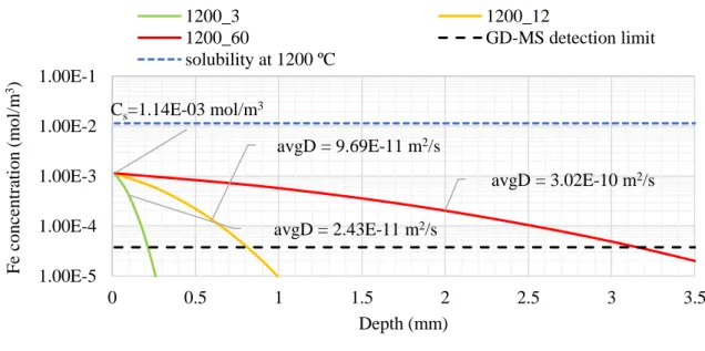
Figure 3.3 - Fe concentration profile, determined based on equation (2.14) starting at 15 μm.
1200_3, 1200_12 and 1200_60 represent a sample treated during 3, 12 and 60 minutes,
respectively, up to 1200 ºC... 25
Figure 3.4 - Ti concentration profile, determined based on equation (2.14), starting at 15 μm.
1350_180 represents a sample treated during 180 minutes, respectively, up to 1350 ºC. ... 26
Figure 3.5 - Representation of the prepared diffusion couples - a) used for Ti; b) focused on
avoiding Fe external sources, with a mono-Si weight replacing the kanthal wire. ... 28
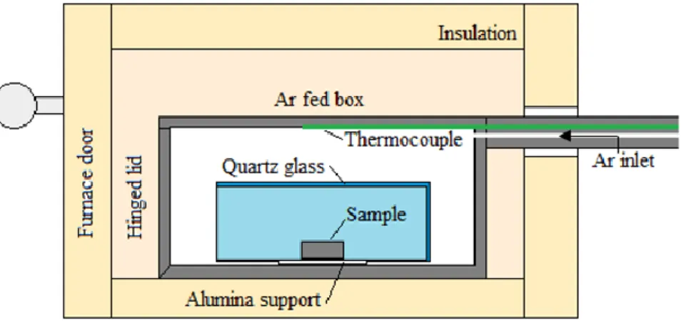
Figure 4.1 - Schematic by Ekstrøm of Nabertherm N17/HR with the sample and quartz glass
crucible inside the argon fed box. ... 29
ix
Figure 4.2 - Iron concentration profiles analysed by Ekstrøm through GD-MS. ... 30
Figure 4.3 - Silicon test samples annealed in Nabertherm LHT 04/18 up to 1200 ºC, during 60
minutes with an argon flow of a) 250 L/h (20 ºC, 300 mbar) b) 500 L/h (20ºC, 300 mbar). .. 31
Figure 4.4 - Schematic of the apparatus with previously used quartz glass crucible: a)
illustration of the argon inlets and components inside the furnace; b) side view for length
comparison of the crucible and furnace interior. ... 31
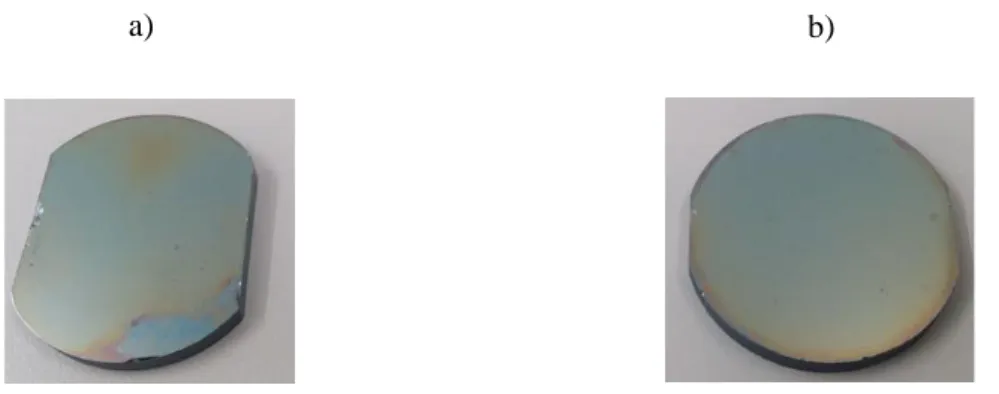
Figure 4.5 - a) Representation of the apparatus with quartz plate; Aspect of the silicon samples
annealed during 60 minutes b) up to 1200 ºC c) until 1350 ºC. ... 32
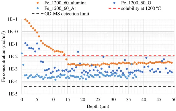
Figure 4.6 - Iron concentration profiles obtained by GD-MS, of couples treated for 60 minutes
up to 1200 ºC. Contains the following samples: Fe_1200_60_KW – diffusion couple held with
kanthal wire; Fe_1200_60 – diffusion couple held with silicon weight. ... 33
Figure 4.7 - Iron concentration profiles obtained by GD-MS of the diffusion couples held with
silicon weight, heated up to 1200 ºC. The following samples are considered: Fe_1200_3 -
treated for 3 minutes; Fe_1200_12 - treated for 12 minutes and Fe_1200_60 - treated for 60
minutes. ... 33
Figure 4.8 - Titanium concentration profiles obtained by GD-MS of the diffusion couple held
with silicon weight: Ti_1200_180 – heated up to 1200 ºC; Ti_1275_180 - heated up to 1350
ºC. Both during 180 minutes and put together with kanthal wire. ... 34
Figure 4.9 - Titanium concentration profiles obtained by GD-MS of the diffusion couple held
with silicon weight: Ti_1350_12 – heated for 12 minutes; Ti_1350_60 - heated for 60 minutes.
Both up to 1350 ºC and put together with kanthal wire. ... 34
Figure 4.10 - Arrhenius fit of scenario 1, for three different Ti compositions in the crucible:
low estimate (0.027 mol/m
3), proposed by manufacturer (0.054 mol/m
3) and high estimate
(0.082 mol/m
3). ... 37
Figure 4.11 - Arrhenius fit of scenario 2, for three different Ti compositions in the crucible:
low estimate (0.027 mol/m
3), proposed by manufacturer (0.054 mol/m
3) and high estimate
(0.082 mol/m
3). ... 37
Figure 4.12 - Arrhenius fit of scenario 3, for three different Ti compositions in the crucible:
low estimate (0.027 mol/m
3), proposed by manufacturer (0.054 mol/m
3) and high estimate
(0.082 mol/m
3). ... 38
Figure 5.1 - Ti concentration profile, determined based on equation (2.14), starting at 15 μm,
for a sample treated during 12 minutes, up to 1350 ºC. ... 40
Figure 5.2 - Curve fitting results of equation (2.14) for the GD-MS profile of the sample heated
up to 1200 ºC during 180 minutes. The curve fit refers to every data point. ... 42
x
Figure 5.3 - Curve fitting results of equation (2.14) for the GD-MS profile of the sample heated
up to 1275 ºC during 180 minutes. Fit refers to every data point, but for fit 2 the profile starts
at the first considered concentration value, taken as the surface. ... 42
Figure 5.4 - Curve fitting results of equation (2.14) for the GD-MS profile of the sample heated
up to 1350 ºC during 60 minutes. The curve fit refers to every data point. ... 42
Figure 5.5 - Curve fitting results of equation (2.14) for the GD-MS profile of the sample heated
up to 1350 ºC during 12 minutes. The curve fit refers to every data point. ... 43
Figure 5.6 - Ti concentration profiles for scenario 1 (GD-MS analysis), scenario 2 (GD-MS
analysis with extrapolation) and scenario 3 (GD-MS analysis with fit). ... 44
Figure 5.7 - Extrapolation of the diffusivity estimates at the GD-MS depth increment, for
scenario 1 and a Ti content in the crucible of 0.027 mol/m
3, by curve fitting a power function.
... 48
Figure 5.8 - Extrapolation of the diffusivity estimates at the GD-MS depth increment, for
scenario 1 and a Ti content in the crucible of 0.054 mol/m
3, by curve fitting a power function.
... 48
Figure 5.9 - Extrapolation of the diffusivity estimates at the GD-MS depth increment, for
scenario 1 and a Ti content in the crucible of 0.082 mol/m
3, by curve fitting a power function.
... 49
Figure 5.10 - The depth profile spectrum of a) a deposited sample; b) a sample annealed at 700
ºC for 1 h in a high vacuum; c) a sample annealed at 650 ºC for 1 h in a high vacuum; d) a
sample annealed at 650 ºC for 8 h in a high vacuum; ACP stands for atomic concentration
percent [78]. ... 51
Figure 5.11 - Comparison of diffusivity estimates from this work (scenario 3 with the high
estimate of Ti in the crucible) and Zhu, et al. 2001 [78]. ... 52
Figure 5.12 - Nabertherm LHT 04/18 rapid heating profile, adapted from [79]. ... 53
Figure 5.13 - Reheating and cooling curves for the different heat treatment temperatures. ... 55
Figure 5.14 - Schematic of the diffusion couple considered in the script. The depth and radius
axis have zeros set in the interface and the dashed centre line, respectively. ... 56
Figure 5.15 - Unidimensional analysis for Ti diffusion in the couple, for the most demanding
scenario. ... 57
Figure 5.16 - Unidimensional analysis for Fe diffusion in the couple, for the most demanding
scenario. ... 58
xi
Figure 5.17 - Comparison of the Fe concentration profiles in the silicon sample, for a wider
interface (20 mm of half-width or radius) where diffusion is unidimensional, relatively to the
effectively employed couples (10 mm of half-width or radius). ... 59
Figure 5.18 - Comparison of the Fe concentration profiles in the silicon sample for the
effectively employed couples, relatively to the average concentration for a circular surface of
7.5 mm radius. ... 59
Figure 7.1 - Diffusion data for iron in silicon. The red profile represents the mean value of the
profiles described in Table 7.1. ... 73
Figure 7.2 - Diffusion data for titanium in silicon. The red profile represents the mean value of
the profiles described in Table 7.2. ... 74
Figure 7.3 - Solubility of iron in silicon. The red profile represents the mean value of the
profiles described in Table 7.3. ... 76
Figure 7.4 - Solubility of titanium in silicon. The red profile represents the mean value of the
profiles described in Table 7.4. ... 77
Figure 7.5 - Extrapolation of the diffusivity estimates at the GD-MS depth increment for
scenario 2 with a Ti content in the crucible of 0.027 mol/m
3, by curve fitting a power function.
... 105
Figure 7.6 - Extrapolation of the diffusivity estimates at the GD-MS depth increment, for
scenario 2 with a Ti content in the crucible of 0.054 mol/m
3, by curve fitting a power function.
... 105
Figure 7.7 - Extrapolation of the diffusivity estimates at the GD-MS depth increment, for
scenario 2 with a Ti content in the crucible of 0.082 mol/m
3, by curve fitting a power function.
... 106
Figure 7.8 - Extrapolation of the diffusivity estimates at the GD-MS depth increment, for
scenario 3 with a Ti content in the crucible of 0.027 mol/m
3, by curve fitting a power function.
... 106
Figure 7.9 - Extrapolation of the diffusivity estimates at the GD-MS depth increment, for
scenario 3 with a Ti content in the crucible of 0.054 mol/m
3, by curve fitting a power function.
... 107
Figure 7.10 - Extrapolation of the diffusivity estimates at the GD-MS depth increment, for
scenario 3 with a Ti content in the crucible of 0.082 mol/m
3, by curve fitting a power function.
... 107
xii
Figure 7.11 - Arrhenius fits of the extrapolated values at scenario 1 and the different Ti
compositions in the crucible: low estimate (0.027 mol/m
3), proposed by manufacturer (0.054
mol/m
3) and high estimate (0.082 mol/m
3). ... 109
Figure 7.12 - Arrhenius fits of the extrapolated values at scenario 2 and the different Ti
compositions in the crucible: low estimate (0.027 mol/m
3), proposed by manufacturer (0.054
mol/m
3) and high estimate (0.082 mol/m
3). ... 109
Figure 7.13 - Arrhenius fits of the extrapolated values at scenario 3 and the different Ti
compositions in the crucible: low estimate (0.027 mol/m
3), proposed by manufacturer (0.054
mol/m
3) and high estimate (0.082 mol/m
3). ... 110
1
1 Introduction
1.1 Motivation
The objective is to characterize the impact of different crucible materials on the contamination of directionally solidified, p-type silicon ingots and study the solid-state diffusion of iron and titanium in a commercial reaction bonded silicon nitride (Si3N4) crucible, a substitute for fused silica crucibles,
currently used in directional solidification (DS).
Silica crucibles are often limited to a single use, since they crack due to a phase transformation while cooling down. Si3N4 crucibles however, can withstand reutilization, present a thermal expansion
coefficient more similar to silicon and are more thermally conductive, which may lessen the energy requirements.
If the crucible is put in contact with other materials, e.g. molten and solid silicon, it may act as a contamination source. When defects such as transition metals are introduced in the silicon crystal lattice, they can enable trap levels between the conduction and valence bands of the semiconductor, promoting the recombination of light generated charge carriers and leading to a curtailment in the conversion efficiency. So far, the knowledge for the diffusion of impurities in Si3N4 is lacking when compared to
more widespread materials. Therefore, achieving data regarding this crucible can support its application in the photovoltaic industry and provide more information for future studies.
1.2 Aim of this work
The study aims to review the current literature on the contamination of DS ingots originating from different crucibles and to determine diffusion coefficients for Fe and Ti in the stated crucible for a range of temperatures by heat treatment of diffusion couples, with Si3N4 and monocrystalline silicon from a
Czochralski ingot, according to Fick’s 2nd law. This method works around ingot casting, while still
aiding the description of the contamination in the solid phase of the ingot during crystallization and subsequent cooling. Concentration vs depth profiles are obtained through direct current - glow discharge mass spectrometry for the silicon sample. The data is taken as an indirect measurement of the amount of impurities originating from the crucible. The resulting profiles are analysed in order to estimate the diffusivities.
2
2 Theory
2.1 Silicon solar cells
The Earth’s crust is mainly constituted by oxygen, followed by silicon, representing 26% of its weight. Its free form does not occur in nature, being instead associated with oxides and silicates, such as in quartz and sand. For solar cells, silicon is preferred with low impurity amounts. Currently, the Siemens deposition can yield 9N (99.9999999%) electronic grade silicon, although purity grades of 6-7N [1] are also produced by feeding monosilane (SiH4) into a fluidised bed reactor with heated silicon particles.
The gas is continuously decomposed, covering each particle’s surface with more silicon, increasing their diameter. These granules can be extracted and added to the bed continuously, while the Siemens deposition is batch reliant, allowing decreased costs [2].
The current methods for silicon feedstock recrystallization are quite extensive and often present specific designs. Nonetheless, silicon based photovoltaic (PV) cells can be solidified in monocrystalline (mono-Si), multicrystalline (mc-Si) or amorphous (a-Si) forms. Mono-Si is presently the most efficient solution (25.3% - FhG-ISE), above mc-Si (21.9% - Fraunhofer-ISE), while excluding concentrator or heterostructure technologies [3].
Single crystal cells derive from the Czochralski (Cz) process, where an ingot is grown by slowly pulling a previously dipped seed in molten silicon. This production rate can be about 2 kg h−1, making the directional solidification of mc-Si an attractive method, since its overall productivity rounds 7 kg h-1.
Other advantage of using DS is lower energy consumption, about 10 kWh kg−1 with Cz surpassing it by more than three times. This incentivizes interest towards mc-Si solar cells due to cost-effectiveness and it is, in fact, the highest market share holder (about 70% of the global PV production in 2015) [4]. To stay competitive, mono-Si needs improvements in the energy demanding manufacture or in the solar cells conversion efficiency, where an increase of 1% could reduce the cell production cost about 7%. The efforts usually focus around hot-zone designs, multiple charges, cheaper and long-lasting crucibles and reduced argon consumption [5].
2.2 Directionally solidified silicon
DS follows the principles of the Bridgman crystallization and is how most mc-Si ingots are produced, in quartz crucibles coated with a mix of α and β-Si3N4 to avoid ingot sticking. This method consists in
inductively heating the silicon charge inside the crucible, followed by a nucleation stage starting at the bottom of the crucible, which is regulated by slowly lowering the crucible out of the hot zone. Mean grain size increases along the ingot height, as result of the competitive growth between adjacent grains, parallel to the thermal gradient (Figure 2.1). Other techniques are also used to make the liquid silicon solidify in a single direction due to a temperature gradient [6].
3
Figure 2.1 - Directional solidification of a mc-Si ingot by the Bridgman technique [6].
Defects in mc-Si from DS can originate from the feedstock, crucible and coating or due to process conditions. These can induce dangling bonds and deep states in the silicon bandgap, promoting the recombination of light generated charge carriers and, therefore, curtailing the conversion efficiency [7]. Dislocations can be found in clusters formed at grain boundaries, spreading into considerable areas of the ingot due to thermal stress while solidifying [6]. They constitute the main source of recombination centres, while stacking faults and twins are usually negligible [7]. Engineering techniques to decrease their amount, during and after crystal growth, were summarized in [7]. The correlation between grain size and minority carrier lifetime is also uncertain, since the grain diameters in mc-Si are usually in the order of mm to cm, larger than the typical minority carrier diffusion length of 100 μm [7].
High performance multicrystalline silicon (hpmc-Si) focuses on generating smaller grains, in the mm2
range, by controlling the nucleation stage. These provide relaxation under thermal stress, supressing the generation and proliferation of dislocations [8]. Fewer dislocation clusters, which improve the gettering efficacy [9], a high fraction of random angle boundaries and a lower twin proportion, contribute to an increase of at least 0.5% in efficiency over traditional mc-Si [10].
2.3 Contaminants in mc-Si
The lower efficiency in mc-Si solar cells, comparatively to mono-Si, is often associated to the limited charge carrier diffusion length, consequence of the increased recombination effect brought by crystalline structural defects and a higher amount of electrically active impurities.
The prevalent impurities are oxygen, carbon and nitrogen [11], but metallic atoms are also common. Sometimes these associate with other defects, aggravating the electrical performance of the cells even further [7], so that the studies focus not only in reduction of the impurity amounts, but also on the density of crystalline defects. As the presently available solar grade silicon feedstock and argon gas, which is employed to provide an inert atmosphere, meet the high purity requirements, the crucible and its coating are regarded the primary sources of contamination for DS mc-Si ingots [12]. Boron doped ingots typically present low minority carrier lifetimes in the top, edge zone and bottom (Figure 2.2):
4
Figure 2.2 - Lifetimes in a cross section of a mc-Si ingot. The red colour highlights areas with shorter lifetimes [13]. At the top, the reduced lifetime is caused by the segregation of transition metals [14], resulting from their typically higher solubility in liquid rather than in solid silicon. As the solid-liquid interface progresses, the concentration in the melt increases, carrying the majority of the impurities towards the top of the solidified ingot [15].The segregation of substitutional impurities (B and Al) has been reported to depend on the grain morphology, according to Scheil's equation (presented in page 7), whilst the melt and the grain boundaries were described as diffusion enhancing paths for interstitial impurities (Fe, Ti, Cu, and Ni), increasing their effective segregation and concentration in irregular grains [16].
Recombination activity at the edges is given by dissolved or diffused impurities, from the crucible walls and coating [14]. When these are kept at high temperatures, faster diffusers, including Fe, are known to migrate into the solid phase [17]. While cooling, both contaminants can spread further into nearby regions, depending on the cooling rate and respective diffusion coefficients [18]. The affected zone also broadens towards the bottom (see Figure 2.2), implying that the earlier solidified sections are subjected to impurity diffusion for longer periods.
Interstitial iron, as well as iron complexes, introduce deep levels in the band gap,increasing the carrier recombination rate. However, the first is more detrimental. Dissolved iron in boron doped silicon primarily occurs as interstitial iron - at temperatures above 200 ºC and boron concentrations below 1016
at/cm3 - and Fe-B pairs - at room temperature and boron concentrations above 1014at/cm3. Interstitial iron precipitates on high angle grain boundaries and dislocations by internal gettering, depleting adjacent areas [14]. In the border region, the dislocation density is much lower than in the vicinity, therefore the content of Fe-B is significantly higher, possibly explaining the low lifetime [7].
A reduction in contamination of fast or moderately fast diffusers, such as Fe, can be achieved by gettering techniques. However, posterior removal is more difficult for slow diffusers incorporated in the ingot, like Ti [13].
In the bottom, lifetime is often affected by oxygen-related defects [14]. Single interstitial oxygen atoms are not electrically active [11], but oxygen precipitates damage the electrical performance, act as internal gettering sinks for other impurities and affect the mechanical properties of the silicon wafers [19]. Oxygen and carbon incorporation has been described to occur according to the following sequence [19]:
5
i. Dissolution of the silica (SiO2) crucible by the melt, introducing oxygen and silicon atoms;
ii. The dissolved oxygen reaches the gas/melt interface, evaporating as silicon monoxide (SiO); iii. The argon gas flow brings SiO to react with the graphite components in the furnace, producing
gaseous carbon monoxide (CO);
iv. These return to the melt surface by diffusion or convection, followed by dissolution; v. Lastly, the dissolved C and O atoms are segregated into the crystal.
Although there are several furnace configurations, the cited graphite components participating in the previous process are usually the heaters, crucible covers and a box that serves to mechanically stabilize the silica crucible, as it softens above 1200 ºC [20], before reaching the silicon melting temperature [21].
The concentration of carbon can influence oxygen precipitation, although, it has been demonstrated that carbon is not detrimental for recombination in substitutional sites [19]. On the other hand, nitrogen has been reported to result from the partial dissolution of the silicon nitride coating by the liquid silicon.It may form lifetime limiting complexes with oxygen near the crucible walls and bottom [11], even though it is usually electrically inactive [19].
The melt flow influences their distribution and also whether the solubility limit of carbon and nitrogen is reached. At that stage, precipitation of silicon carbide (SiC) and Si3N4 can occur [11], eventually
promoting the nucleation of new grains [19]. SiC can cause severe ohmic shunts in solar cells and sometimes grow several mm along the direction of crystallization, therefore harming several wafers. Due to their hardness, they can also affect the sawing process and the production yield. Si3N4 precipitates
are insulating, but might be decorated by impurities and surrounded by decorated dislocations, affecting the electric performance of solar cells [21].
2.3.1 Schockley-Read-Hall recombination
When introduced in the silicon crystal lattice, defects can enable trap levels between the conduction and valence bands of the semiconductor.
Research in interstitial titanium has identified an acceptor level at 𝐸𝑐– (0.08 − 0.09) eV with the charge state Ti𝑖−/0and two donor levels at 𝐸𝑐– (0.27 − 0.28) eV with Ti𝑖
0/+
and at 𝐸𝑣+ (0.25 − 0.28) eV with Ti𝑖+/++. Interstitial iron introduces a donor level at 𝐸𝑣+ (0.39 − 0.40) eV for the charge state Fe𝑖0/+ and in p-type silicon, mobile atoms with positive charge are captured by negatively charged substitutional acceptor atoms to form iron-acceptor pairs. The frequent Fe-B pairs introduce a donor level at 𝐸𝑣+ 0.19 eV [22]. These states promote an indirect recombination mechanism of electron-hole pairs, designated as Shockley-Read-Hall (SRH), where an electron (or hole) is captured at the trap level and a hole (or electron) moves into the same energy level, before the first carrier thermally returns to its previous state. Figure 2.3 illustrates the recombination in four parts [23]:
i.
Electron capture – an electron from the conduction band moves to the trap level;ii.
Electron emission – an electron from the trap level jumps to the conduction band;iii.
Hole capture - an electron from the trap level moves to the valence band (the hole disappears);iv.
Hole emission – an electron from the valence band jumps to the trap level (a hole is formed).6
Figure 2.3 - Scheme of the processes in SRH recombination [23].
When light is absorbed in the solar cell, within or at a certain distance from the depletion region, electron-hole pairs are generated. For a p-n junction in a steady state, this depletion region is formed by the diffusion of holes towards the n-doped side (excess of free electrons), leaving their respective negative acceptors behind, whilst electrons move in the opposite sense, towards the p-doped side (excess of holes), also leaving their respective holes. These diffused oppositely charged carriers eventually meet in their way across the junction and recombine, creating an interface without free holes and electrons, designated depletion region (Figure 2.4).
Figure 2.4 - A p–n junction in steady state with no applied voltage. The grey regions represent neutrally charged parts of the
semiconductor [24].
The remaining charges stay separated by this region, since they create an electric field that provides enough opposing force to stop recombination and is responsible for the built-in voltage [25].
To contribute to the useful current, these carriers must then be collected by the p-n junction. If the pair splits within the depletion region, the electric field quickly pulls them apart and collection occurs. However, in the other sections the charge carriers must diffuse towards the p-n junction. The average length they are able to cross within the material until recombining is termed diffusion length, a parameter influenced by carrier lifetime, which is partially affected by the recombination rate. Therefore, the
7
presence of SRH recombination centres, diminishes the likelihood of a carrier reaching the junction and consequently decreases the conversion efficiency of the solar cell [26].
2.3.2 Impact of Fe and Ti in feedstock for DS mc-Si
Several ingots were prepared to evaluate the impact of transition metals on solar cell performance, including iron and titanium [27]. A reference ingot was doped with boron (0.13 ppmw) and compared to others, to which certain amounts of impurities were added intentionally. Unintentional contamination was assumed to be minimal and the same for every ingot, since high purity polysilicon feedstock, fused quartz crucibles and silicon nitride coating were used.
Fe was introduced before melting with the feedstock but Ti was added after complete melting, given its susceptibility to form oxides at lower temperatures.
The contamination levels were chosen targeting typical amounts present in silicon ingots. Two ingots, labelled Fe 50 and Fe 200, were grown with added concentrations of 53 ppmw and 200 ppmw of Fe, respectively. Similarly, another was prepared with 9.3 ppmw of Ti and labelled Ti 10. Wafers were cut from selected positions of the ingots and went through similar state-of-the-art solar cell industrial processing, regardless of the contamination.
The experimental data was fit successfully to two validated models based on Scheil’s distribution1, to
describe the whole ingots. Cell performance was determined as a function of base-bulk and emitter-bulk recombination, as shown in Figure 2.5.
All contaminated cells, including others prepared with Cr, Cu, and Ni, have performances comparable to the reference in the 40-70% ingot height section. The regions below (ingot bottom) and above (ingot top) present lower efficiencies.
Contaminated ingots present an extended degradation near the bottom, while in the reference it reaches about 10% of the height. In a previous report for Fe 50 [28], smaller grains and highly dislocated areas were detected. This work went further, demonstrating that it also happens with Cr, Ni and Cu, with higher feedstock concentrations accentuating the degradation. The performance at the top of the ingots also suffers due to this increase and is result of the phenomena described above. Ti was so detrimental to the efficiency that the curtailments were difficult to discern. Based on the analysis, it was summarized that 8 ppmw of Cr, 11 ppmw of Fe, 0.1 ppmw of Ti, 4 ppmw of Ni or 8 ppmw of Cu resulted in solar cells with similar performances when prepared in the same conditions, regardless of the influence of other parameters. The lower amount of Ti illustrates the need to avoid contamination of the ingot, given the limited getterability brought by the slow diffusivity.
1Solute concentration profile along the ingot, according to the following equation, which describes the segregation during
solidification, assuming that no diffusion exists in the solid phase once it is formed, infinitely fast diffusion occurs in the liquid phase and that the solid-liquid interface is in equilibrium:
𝐶𝑠= 𝑘 𝐶𝑚(1 − 𝑓𝑠)𝑘−1
𝐶𝑠 and 𝐶𝑚 stand for the concentration in the solid phase and in the melt, respectively, 𝑘 is the effective segregation coefficient
8
Figure 2.5 - Solar cell efficiency versus ingot position from the bottom: a) Cells from the ingots contaminated with 53 and
200 ppmw of Fe; b) Cells from the ingot contaminated with 10 ppmw of Ti. Cu 100 was also studied in the work, an ingot contaminated with 100 ppmw of Cu (adapted from [13]).
2.4 Directional solidification crucibles
2.4.1 Silica
As of the day, silica crucibles, also often designated as quartz or amorphous silica, are the most used in solar cell manufacture, due to the requirements put on by the high melting point (1412 ºC) of silicon, the reactivity of its molten phase, the heat induced stress and the availability of high purity feedstock [29].
They can be synthesized by many procedures, most of them confidential, especially for crucibles not used for directional solidification. For DS crucibles, the chain starts at the extraction of high purity crystalline quartz, usually followed by processing to increase this purity even further. The sand is electrically fused into silica glass which is afterwards turned into a powder that is sintered, meaning that it is mixed with water and a binder to form fused silica slurry [30]. The slurry is moulded and goes through several moisture absorption steps and annealing at high temperatures finalizing the production of the crucibles with the aspect seen in Figure 2.6.
9
Figure 2.6 - Fused silica ceramic crucible manufactured by SOLAR CERA Co., Ltd. for directional solidification of mc-Si
[31].
Although in Cz production the ingot is not contact with the crucible, that does not happen for DS. It solidifies in contact with silica, which might be wetted by the molten silicon, creating such a strong adherence, that the crucible must be broken to free the contained ingot (Figure 2.7).
Figure 2.7 - A small mc-Si ingot grown in a fused silica crucible without coating. The wetting by molten silicon caused
considerable sticking [32].
Furthermore, silicon has a higher thermal expansion coefficient in comparison with silica, which while cooling translates into a more pronounced shrinkage in silicon, than in the crucible. If simultaneously met by wetting, both may induce enough stress to form cracks in the ingot [33]. To avoid this, it is a common practice to apply a uniform coating of silicon nitride (α or β-Si3N4), with specific particle size
and distribution, that decreases the wetting effect and also lowers the contamination from the crucible. The latter justifies its use in crucibles for Cz pulling, in order to achieve better quality ingots [29]. Another factor contributing to crucible failure while cooling is the phase transformation occurring in silica. In the melting stage, with temperatures over 1470 ºC, or others depending on the pressure, part of the silica is transformed from a glassy α-quartz phase into a more stable layer of another silica polymorph in those conditions, β-cristobalite (Figure 2.8). This layer has a cubic crystal structure and a melting point of 1713 ºC, above the peak registered in the furnace, aiding the integrity of the crucible. In the post-solidification cooling, this phase undergoes a new transition, from β to α-cristobalite, with a tetragonal structure, leading to a decrease in volume of around 5% and cracking the layer. In normal conditions, the crucible also deforms due to the cooling stage, both contributing to break the crucible so that it cannot be reutilized [29, 34].
10
Figure 2.8 - Phase diagram of the silica polymorphs, based on Swamy and Saxena (1994) [35].
2.4.1.1 Decreasing contamination during DS in SiO
2crucibles
Several efforts accounting for O and C contamination in DS mc-Si have been published, considering for instance heater positioning and heating power, crucible rotation, argon atmosphere pressure and crucible covers. In addition, the role of crucible and coating purity level and the effect of an alternating magnetic field on metallic elements distribution have been analysed.
Melt convection and diffusion are said to be relatable to the oxygen distribution, both in the silicon melt and ingot [36]. A simulation was carried, suggesting that melt content would be smaller for a side heating system, as opposed to a system with only top heating. This was explained to be consequence of an upwards melt flow near the crucible wall when side heating is used. The dissolved oxygen from the silica crucible quickly reaches the melt surface, followed by evaporation [37].
Another numerical study refers to the influence of the temperatures inside the furnace, during the holding phase, on the melt contents of carbon and oxygen. An increased temperature enhances oxygen evaporation from the melt surface, promoting the reaction of SiO with the graphite components, forming CO. If this gas is not drawn out before reaching the liquid silicon, the carbon content will be higher. An accordingly warmer crucible also accelerates the oxygen dissolution by the melt. This increase is not compensated by the enhanced evaporation rate, leading to a superior oxygen amount in the molten phase. Hence, the furnace temperature should be kept as low as possible to minimize the contamination of the ingot by these elements [38].
The effect rotation speed of the crucible rotation on oxygen concentration was also studied numerically [36, 39] and reported in a cylindrical ingot, with 10 cm of diameter and height [36]. The results show that increasing crucible rotation leads to higher oxygen content in the melt, when taking into account the balance between evaporation from the melt surface and crucible dissolution. The evaporation slows down at a quicker rate than the dissolution, so that the oxygen present in the melt increases [39].
11
Regarding the oxygen distribution in the cylindrical ingot, increasing crucible rotation yields higher concentrations near the top and middle of the ingot, although the distribution should be inhomogeneous among the radial direction. When an ingot was grown at a rotation rate of 1 rpm, the oxygen concentration was homogenized throughout the radius and minimized in the whole ingot, in comparison with another prepared with a rotation rate of 30 rpm [36].
The use of a crucible cover was suggested to reduce the carbon contamination. Based on the multiple previous numerical models for the transport of O and C in DS [40], comprised a transient global simulation of these mechanisms in the melt, furnace atmosphere and the segregation during the solidification, to estimate the impurity distribution in an industrial-size ingot. The numerical predictions illustrated that applying an inert coating to a pure graphite cover could reduce the C concentration in the ingot by about 60%, although there was no significant difference for oxygen. Afterwards, comparisons were made with the C concentration in a prepared ingot, agreeing to a reasonable extent with the simulation results [40]. Additionally, cover usage was reported to diminish the oxygen amount near the top of the ingot, due to an enhanced gas flow promoting the evaporation of oxygen from the melt surface. This was concluded accounting a gradually decreasing distribution, from top to bottom, obtained without cover [19].
Other numerical analysis, verified experimentally, sought to explain the influence of pressure in an industrial furnace. It was found that it affects the argon flow above the melt surface, altering the transport of the SiO and CO gases. Lower pressure yields less O concentration in the grown ingot, while for C it shows a decreasing trend until 200 mbar. For lower pressures, it starts increasing due to CO diffusion through a gap between the crucible and respective cover, present in this furnace. It is then worthy to determine at what point the pressure may be decreased avoiding drawbacks [41].
Not only oxygen is introduced in the melt by dissolution, but also nitrogen and other impurities are likely to be dissolved or diffuse out from the coating and crucible [20]. Addressing crucible and coating purity levels, [15] elucidated that this property is relevant for minority carrier lifetime in the ingot, with experiments depicting a doubled lifetime when a highly-pure quartz crucible and coating were chosen instead of the industrial standard. Applying a sufficiently thick layer of high-purity silica on standard-purity crucible, prior to the deposition of silicon nitride coating, may provide a diffusion barrier and thence improved lifetime measurements. Other configuration was tested with a silica film deposited over of the silicon nitride coating, aiming to supply producers with already coated crucibles. The silicon melt was able to dissolve more oxygen, due to contact with the silica coating, leading to ingots with acceptable lifetimes and higher oxygen content [15].
Increased carrier lifetimes were also achieved in ingots grown with high-purity silica crucibles, as opposed to standard industrial crucibles, using similar silicon nitride coatings. The thickness of the low-lifetime edge region was decreased and the improved regions coincided with lower concentrations of interstitial iron. The Fe content in the crucible seemed to influence diffusion from the silicon nitride coating, determining whether it behaved as an infinite source, for the standard crucible, or depletable source, when using the high-purity alternative [12].
At last, in research done for metallurgical grade silicon, multicrystalline ingots were obtained with and without an alternating magnetic field during an industrial DS process. The less contaminated areas of the ingots showed lower concentration of metallic impurities when the alternating magnetic field was used, since it induced a convection capable of limiting the diffusion of those impurities in the melt, resulting in decreased effective segregation coefficients [42].
12
The stated cons for fused silica crucibles brought attempts to find alternatives that may be reused in DS, ensuring high purity, low chemical reactivity with molten silicon and a thermal expansion coefficient that does not generate mechanical tensions between ingot and crucible while cooling down. The research started decades ago, with interest in many materials, some among them were graphite crucibles coated with SiC or Si3N4 [43], moulded graphite sheets coated with silicon oxynitride [44], Si3N4 crucibles [33,
45, 46, 47] and recently a composite of Si3N4 and SiO2 [48].
The reports on these alternative crucible materials for the DS of silicon ingots do not address the contamination by distinct elements, placing more focus on crystalline structure and resistivity analysis, hindering the comparison with silica crucibles and their role on the electrical performance of the resulting ingots. The graphite crucibles [43, 44] refer to earlier stages of development in the industry, both in terms of material purity and solidification technique. Meanwhile, the composite of Si3N4 and
SiO2 [48] comprises a simulation of the growth process, according to the thermophysical properties of
the crucible, and photoluminescence analysis of the grain structures from prepared ingots. Hence, besides SiO2, most knowledge comprises Si3N4 crucibles.
2.4.2 Silicon nitride
The wide array of configurations aiming to achieve desirable characteristics is evident for quartz based products at our disposal these days. Silicon nitride is not different, as many routes can be taken to meet requirements and multiple inventors came up with their own versions. For this subject, interest is turned towards Si3N4 options who can fulfil the previously enounced requirements.
Most often, reaction bonded silicon nitride (RBSN) is selected for fabrication of crucibles, as these can be produced without requiring a binding agent, thereby avoiding a reported contamination source [20]. It is produced by casting a slurry with silicon powder and heating it in a controlled nitrogen atmosphere at around 1200 ºC [49]. Nitrogen permeates the pores between the grains and reacts with the silicon. Afterwards, the temperature is increased close to the silicon melting point. The process can take up to two weeks, resulting in a ceramic weighing 60% more than the original powder due to the added nitrogen, with almost no volume change. The use of sintering aids in its processing may also provide strength and creep resistance at high-temperatures [49].
The development of RBSN was summarized in [33], started by JP-59-162199, where RBSN crucibles were designed to achieve coefficients of thermal expansion comparable to the silicon ingots. These had 85% of the theoretical maximum density for silicon nitride and good mechanical strength. However, problems with wetting and consequent adherence led to crucible cracking.
This was addressed by [45] where regulated particle size distribution of the silicon particles and pressure during nitriding allowed to produce silicon nitride with a density between 40 and 60% of the theoretical maximum and at least 50% of the pores of the crucible surface with larger diameter than the mean particle size of the Si3N4 particles.
These crucibles showed no tendency for wetting phenomena, except for regions with open porosity below 40%, allowing a relatively easy release of the ingot from the crucible. Reusability was also reported in [46] for 30 cm x 30 cm square cross section RBSN crucibles, with a wall 25 mm thick and a Si3N4 release coating. Sixteen crack-free ingots were cast in a heat exchange method furnace using the
same mould.
The potential of silicon nitride crucibles was studied in [50], verifying the influence of their thermal properties during mc-Si solidification in a Bridgman furnace, demonstrating that the lower thermal resistivity of the silicon nitride, in comparison with silica, led to more heat loss through the crucible
13
bottom, prolonging melting time but accelerating solidification. This conclusion led to the replacement of the two carbon fibre discs underneath the crucible by better insulating alumina fibre material, shortening the melting and solidification times in favour of lower energy requirements. Allied with reusability, as seen in Figure 2.9, a so sought cost reduction might be possible.
Figure 2.9 - a) Ingot solidified in the silicon nitride crucible, under the optimized thermal conditions; b) shows the
detachment was successful, without major signs of wetting [50].
Similar results have been also claimed in [51], but it was also observed that using a crucible with large thermal conductivity may be responsible for a more pronounced concave shape in the melt-crystal interface and a high temperature gradient in the ingot, increasing the chance of thermal stress and propagation of dislocations. Based on further analysis, [48] presented the Si3N4 and SiO2 composite
design based on the knowledge that the crucible bottom wall regulates the vertical heat release, whereas the side wall influences the horizontal heat flux, related to the stated melt-crystal interface shape. Analysis of ingots prepared with Si3N4 crucibles with different purity grades, Si3N4 coating firing
procedures and holding temperatures in the melting stage can be found in [52]. The results were compared to reference ingots cast in silica crucibles, accounting for the dissolved oxygen and dopant elements distributions along the ingot height.
It has been reported that the dissolved oxygen concentration in the bottom of the ingots depends directly on the holding temperature when melting the silicon charge, but no relationship was found between the bottom contamination and the crucible material used. There were although other parameters that could contribute to this, such as the thermal gradient, given that silicon nitride crucibles are more heat conductive than others made of silica. The concentration decreased towards the top in all ingots, however, the decrease was steeper for the silicon nitride crucibles, in comparison with SiO2 crucibles.
The authors’ reasoning for this is the possibility of having different sources for oxygen in the two crucible materials, a silicon oxynitride layer in Si3N4 crucibles, as diffusion seemed to decline over
solidification time, and a silicon oxide layer in the silica counterparts, where the diffusion was more stable.
To avoid wetting, the coating is applied and fired in an oxidizing atmosphere. Trying to keep the oxygen content in the coating layer low, the experiments included firing at 900 and 1100 ºC in a mixture of air and N2, while the remaining parameters were as close to each other as possible. The resulting ingot
contamination made it evident that lower firing temperatures decreased the dissolved oxygen concentration, supporting the claims of [53], however this happened at the cost of severe sticking.
14
The boron and phosphorous contents in the Si3N4 crucibles were considered before applying the coating.
Boron is believed to be present at this stage as boron-nitrides. After coating, the firing can oxidize them partially, forming boron-oxides. Phosphorus oxides should also occur. Both are volatile at the melting temperature of silicon, therefore may diffuse through the coating into the ingot. Conversely, the remaining boron-nitrides should stay solid below 3000 K. The vapour pressure of the phosphorus-oxides is described as significantly superior to the boron-nitrides, respectively in the order of 10-3 atm and 1
atm, so that after some runs, the phosphorus ingot contamination is drastically reduced, due to evaporation from the crucible. Meanwhile, boron is less prone to evaporation, so the variation in the ingot should be less noticeable, justifying the choice of a crucible material with less boron content to limit ingot contamination throughout the crucible reutilization [52].
Improvement of the raw material purity was also pointed out in [20], regarding a nitride bonded silicon nitride (NBSN) crucible. Changes to the crucible manufacturing or a cleaning run were also proposed as alternatives. Six ingots of undoped DS mc-Si were produced, demonstrating similar concentrations of interstitial oxygen and substitutional carbon in comparison to a standard fused silica crucible. The authors underlined that those six runs almost reached the cost efficiency of the fused silica crucibles. The level of ingot contamination also decreased after re-running. In this case, the dominant impurities were boron, aluminium and phosphorus, based on a comparison of measured and calculated resistivities. An estimate of their diffusion length during the growth process ruled out solid state diffusion as the dominant mechanism of contamination for the ingot bulk. Additionally, the volume change, prior and after to the growth process, was too small be responsible for the introduction of the measured impurities, thereby, the dissolution of the crucible by the melt was also not the major form of contamination. It was attributed instead to out-diffusion from the NBSN crucible into the molten silicon, relying in a model, with the melt behaving as an infinite sink. The B, Al and P atoms were transported in the melt by diffusion and convection, followed by segregation into the ingot. Noticeably, the literature lacks data regarding the diffusivity of these elements for materials similar to the NBSN crucible, so the simulation reached those diffusion coefficients considering the impurity concentrations in the ingot. Although the estimated orders of magnitude were plausible, a comparison with more data could further support their claim.
Currently, the silicon nitride crucibles have not been implemented industrially. This is probably because there is no clear evidence that reusability can lead to a cost reduction, in comparison with the widespread fused silica, or due to the effect of these crucibles on ingot contamination [20].
2.5 Impurity Transport
2.5.1 Macroscopic diffusion
In solids, atomic positions are dictated by the most energetically favourable sites. At 0 K, the atoms remain at their lattice sites, but if temperature increases, they will vibrate around the sites due to thermal agitation. Eventually there is enough available energy to allow atoms to move into other energetically favourable site.
In a homogeneous distribution, without applied external forces, this random migration does not disturb the equilibrium, since on average the fluctuations cancel out. Nonetheless, for an inhomogeneous placement, atoms gradually rearrange themselves following the chemical potential gradient until equilibrium is established. This mechanism has been designated diffusion and described both with phenomenological (or macroscopic) and atomistic (or microscopic) approaches.
![Figure 2.1 - Directional solidification of a mc-Si ingot by the Bridgman technique [6].](https://thumb-eu.123doks.com/thumbv2/123dok_br/15613348.1053971/17.892.228.628.120.352/figure-directional-solidification-mc-si-ingot-bridgman-technique.webp)
![Figure 2.4 - A p–n junction in steady state with no applied voltage. The grey regions represent neutrally charged parts of the semiconductor [24]](https://thumb-eu.123doks.com/thumbv2/123dok_br/15613348.1053971/20.892.163.735.551.906/figure-junction-applied-voltage-regions-represent-neutrally-semiconductor.webp)
![Figure 2.6 - Fused silica ceramic crucible manufactured by SOLAR CERA Co., Ltd. for directional solidification of mc-Si [31]](https://thumb-eu.123doks.com/thumbv2/123dok_br/15613348.1053971/23.892.240.653.107.376/figure-fused-silica-ceramic-crucible-manufactured-directional-solidification.webp)
![Figure 2.8 - Phase diagram of the silica polymorphs, based on Swamy and Saxena (1994) [35]](https://thumb-eu.123doks.com/thumbv2/123dok_br/15613348.1053971/24.892.246.646.111.523/figure-phase-diagram-silica-polymorphs-based-swamy-saxena.webp)