Universidade de Aveiro
2010
Departamento de Electrónica e Telecomunicações
Paulo
Miguel
Madureira
Martins
Comunicações e armazenamento de massa em
sistemas embebidos escaláveis
Universidade de Aveiro
2010
Departamento de Electrónica e Telecomunicações
Paulo
Miguel
Madureira
Martins
Comunicações e armazenamento de massa em
sistemas embebidos escaláveis
Communications and mass storage in scalable embedded systems
Dissertação apresentada à Universidade de Aveiro para cumprimento dos requisitos necessários à obtenção do grau de Mestre em Engenharia Electrónica e Telecomunicações (M.I.E.E.T.), realizada sob a orientação científica do Prof. Dr. Manuel Bernardo Salvador Cunha e do Prof. Dr. José Luis Costa Pinto Azevedo, Professores Auxiliares do Departamento de Electrónica Telecomunicações e Informática da Universidade de Aveiro
Dedico este trabalho à minha namorada e filho pelo incansável apoio, e ao Pedro Kulzer por acreditar na capacidade do grupo com quem trabalhei e por ter tido uma atitude sempre positiva face às adversidades que encontramos. Não poderia deixar de agradecer também ao Prof. Doutor Bernardo Cunha pela ajuda prestada no desenvolvimento de soluções e conceitos no decorrer do projecto, cuja contribuição foi fundamental para ultrapassar questões de natureza ténica e cinetífica.
Gostaria de deixar o meu agradecimento ao grupo de trabalho, pelo excelente ambiente e camaradagem que se verificou durante o decorrer do projecto, proporcionando a melhor experiência de trabalho até à presente data.
o júri
Presidente Prof. Doutor António Manuel Brito Ferrari Almeida Professor Catedrático da Universidade de Aveiro
Arguente Prof. Doutor Paulo Francisco da Silva Cardoso
Professor Auxiliar no Departamento de Electrónica Industrial da Universidade do Minho
Orientador Prof. Doutor Manuel Bernardo Salvador Cunha Professor Auxiliar no Departamento do DETI
Co-orientador Prof. Doutor José Luís Costa Pinto de Azevedo Professor Auxiliar no Departamento do DETI
palavras-chave Sistemas Embebidos, Sistemas Integrados, Armazenamento de Massa, Comunicações, USB, FPGA, Xilinx, Spartan 3E
resumo Inserido no projecto ECU2010, este documento visa determinar a melhor
solução possível para implementação de armazenamento de informação e comunicações de elevado débito para aplicações no âmbito do desporto automóvel.
O projecto ECU2010 tem como objectivo a pesquisa de uma nova arquitectura de unidades de controlo electrónico (ECU) para desporto automóvel
especialmente centrado no controlo de motores de combustão interna. A nova arquitectura proposta deverá de ser capaz de fazer o controlo de um motor de combustão interna usando os mais modernos modelos de controlo, mas sendo baseada numa modelo de processamento distribuído, composta por módulos de processamento auto-suficientes ao nível de comunicações e armazenamento e de sensores/actuadores com inteligência capazes de processamento prévio de dados.
A comunicação entre módulos não será abordada neste documento nem a comunicação com os elementos periféricos de actuação e/ou natureza sensorial, mas sim a comunicação entre os módulos de processamento e um dispositivo de controlo e monitorização, doravante chamado de Anfitrião, que tipicamente será um computador pessoal ou PDA.
De igual forma este documento debruçar-se-á sobre uma solução para o armazenamento em massa de informação, principalmente focada no
armazenamento de dados históricos resultantes de variáveis de monitorização, processamento intermédio e de actuação.
O objectivo deste documento será produzir um conjunto de blocos de electrónica digital reconfiguráveis implementando as funcionalidades atrás mencionadas numa FPGA da Xilinx modelo Spartan 3E, que em conjunto com hardware desenvolvido para o efeito fazem a interface com os dispositivos de suporte e comunicação definidos no documento.
keywords Embedded systems, Integrated systems, mass storage, communications, USB, FPGA, Xilinx, Spartan 3E
abstract This dissertation is written in the scope of ECU2010 project, and aims to
determine the best possible solution for information storage and high speed communications for automotive motorsports applications.
The ECU2010 is centred on the research of a new architecture of electronic control units (ECU) for motor sport, focussing on control of internal combustion engines.
The proposed new architecture should be capable of controlling an internal combustion engine using the state-of-the art control models, but based on a distributed processing model consisting on self-sufficient processing modules in terms of communications, storage and intelligent enabled sensors/actuators, which of which is able to produce low-level data processing.
Communication between modules is not discussed herein, neither
communication with the peripheral sensors/actuators. Instead, focus will be given to the communication between the processing modules and a control and monitoring device, hereinafter called the Host, that will be typically a personal computer or PDA.
This document will analyse and propose a solution for information mass storage and retrieval to a host system, mainly focused on historical data produced by variable monitoring and processing. The purpose of this document outcome is to produce a set of reconfigurable digital electronic IP cores,
Table of contents
1 Introduction ...11 1.1 Summary ...11 1.2 Guidelines ...11 1.3 Motivation ...12 1.4 Objectives ...13 1.4.1 General guidelines...13 1.4.2 Non-volatile storage ...15 1.4.3 Wired communications ...15 1.4.4 Wireless communications ...15 1.5 Organization ...162 Analysis of possible solutions ...17
2.1 Summary ...17 2.2 Mass storage ...17 2.2.1 Flash cards ...18 2.2.2 Conclusion...19 2.3 Communications ...20 2.3.1 Wired communications ...20 2.3.1.1 IEEE 1394 Fire-wire ...20 2.3.1.2 USB ...21 2.3.1.3 IEEE 802.3 Ethernet ...21
2.3.2 Wired communications conclusions ...22
2.4 Wireless communications...23
2.4.1 IEEE 802.11 WLAN ...23
2.4.2 Bluetooth ...24
2.4.3 ZigBee ...24
2.4.4 Nordic Semi nRF24L01...25
2.4.5 Wireless communications conclusions ...25
3.1 Mass storage ...29
3.1.1 MMC Electrical Standard, Standard Capacity (MMCA 4.1) ...29
3.1.1.1 Introduction ...29
3.1.1.2 MMC Registers ...30
3.1.1.3 MMC Transfers ...30
3.1.1.4 MMC Token format ...32
3.1.2 Mass storage overview ...35
3.1.2.1 MMC block cache ...36
3.1.2.2 MMC controller ...36
3.1.2.3 Command handler ...37
3.1.2.4 Data handler...37
3.1.3 Mass storage details ...38
3.1.3.1 MMC block cache ...38
3.1.3.2 MMC controller ...42
3.1.3.3 Command handler ...47
3.1.3.4 Data handler...51
3.1.4 Mass storage operation ...55
3.1.4.1 Summary ...55
3.1.4.2 Interface signals ...56
3.1.4.3 Initialization...57
3.1.4.4 Block read ...58
3.1.4.5 Block write ...58
3.1.5 MMC host detailed schematic ...59
3.2 Wired communications ...61
3.2.1 Universal Serial Bus Specification Revision 2.0...61
3.2.1.1 USB Features ...61
3.2.1.2 Bus topology ...62
3.2.1.3 USB Host ...65
3.2.1.5 USB communication model ...67
3.2.1.6 Bus protocol ...68
3.2.1.7 Error detection and handling ...68
3.2.1.8 Device attachment, removal and enumeration ...68
3.2.1.9 Data flow types ...69
3.2.1.10 Device endpoints ...69
3.2.2 Wired communications overview ...71
3.2.2.1 Cellular ECU wired communications scalability ...72
3.2.2.2 USB peripheral IC (CY7C68013) ...73
3.2.2.3 USB interface...74
3.2.2.4 USB client software ...75
3.2.3 Wired communications details ...76
3.2.3.1 USB peripheral IC (CY7C68013) ...76
3.2.3.2 USB interface – FIFO controller ...82
3.2.3.3 USB interface – Slave FIFO read FSM ...83
3.2.3.4 USB interface – Slave FIFO write FSM ...84
3.2.3.5 USB interface – Endpoint FIFO ...86
3.2.3.6 Client software ...87
3.2.4 USB Interface operation ...88
3.2.4.1 Summary ...88
3.2.4.2 Interface signals ...88
3.2.4.3 Initialization...90
3.2.4.4 Endpoint read ...90
3.2.4.5 Endpoint write...90
3.2.5 USB Interface detailed schematic ...91
3.3 Wireless communications...92
3.3.1 nRF24L01 Product Specification ...92
3.3.1.1 Radio features ...92
3.3.2 Wireless communications overview ...93 3.3.2.1 nRF24L01 ...94 3.3.2.2 Payload cache...95 3.3.2.3 Payload flags ...95 3.3.2.4 RF processor ...96 3.3.2.5 SPI master ...97 3.3.2.6 Command parser ...97 3.3.2.7 Setup FSM ...97 3.3.2.8 Configure FSM ...98 3.3.2.9 Receive FSM ...98 3.3.2.10 Transmit FSM ...98 3.3.2.11 Arbiter FSM ...99
3.3.3 Wireless communications details ... 100
3.3.3.1 nRF24L01 ... 100 3.3.3.2 Payload cache... 102 3.3.3.3 Payload flags ... 104 3.3.3.4 RF processor ... 106 3.3.3.5 SPI master ... 109 3.3.3.6 Command parser ... 111 3.3.3.7 Setup FSM ... 113 3.3.3.8 Configure FSM ... 114 3.3.3.9 Receive FSM ... 115 3.3.3.10 Transmit FSM ... 115 3.3.3.11 Arbiter FSM ... 115
3.3.4 Wireless communications operation ... 117
3.3.4.1 Summary ... 117
3.3.5 Wireless communications detailed schematic ... 119
4 Results... 121
4.2 MMC host ... 121
4.2.1 Performance ... 121
4.2.2 Resource consumption ... 122
4.3 USB device ... 123
4.3.1 Performance ... 123
4.3.1.1 Single device @ Root hub ... 123
4.3.1.2 Multiple devices @ Root hub ... 123
4.3.1.3 Multiple devices @ Hub... 123
4.3.1.4 Overall performance ... 124
4.3.2 USB Interface resource consumption ... 125
4.4 Wireless communications... 126 4.4.1 Performance ... 126 4.4.2 Resource consumption ... 126 5 Conclusions ... 129 5.1 Summary ... 129 5.2 MMC Host ... 129 5.3 USB peripheral ... 129 5.4 Wireless communications... 129
Table of figures
Figure 1 - Proposed ECU architecture ...14
Figure 2 - IEEE 802.11g channels (8) ...23
Figure 3 - 802.11g spectral mask (8) ...24
Figure 4 - ZigBee channel distribution (11) ...24
Figure 5 - nRF24L01 channel distribution (1Mbps mode) (11)...25
Figure 6 - nRF24L01 vs. ZigBee communication efficiency (11) ...26
Figure 7 - MMC card architecture (15) ...29
Figure 8 - Sequential reads (15) ...31
Figure 9 - Block reads (15) ...31
Figure 10 - Sequential write (15) ...31
Figure 11 - Block write (15) ...32
Figure 12 - No response and no data transfers (15) ...32
Figure 13 - Command token format (15) ...32
Figure 14 - Response token format (15)...33
Figure 15 – 1-bit, 4-bit and 8-bit data packet format (15) ...34
Figure 16 - Mass storage overview ...35
Figure 17 - MMC host overview ...35
Figure 18 – MMC block cache overview...36
Figure 19 - MMC Controller overview ...36
Figure 20 – Command handler overview ...37
Figure 21 - Data handler overview ...37
Figure 22 - MMC block cache interface...38
Figure 23 – 2048 x 8 bit Dual Port RAM ...40
Figure 24 – Xilinx ISE Block Memory Generator ...40
Figure 25 - MMC cache detail ...40
Figure 26 - MMC block cache read timing ...41
Figure 27 - MMC block cache write timing...41
Figure 29 - MultimediaCard state diagram (card identification mode) ...44
Figure 30 - MMC controller initialization ...45
Figure 31 - Block Read ...46
Figure 32 - Block Write ...46
Figure 33 - Command handler interface signals ...47
Figure 34 - Command handler overview ...48
Figure 35 - CRC7 generator ...49
Figure 36 - Data handler interface signals ...51
Figure 37 - Data handler overview ...53
Figure 38 - CRC16 generator ...54
Figure 39 – MMC host interface signals ...56
Figure 40 - MMC host initialization signal sequence ...58
Figure 41 - Block read signal sequence ...58
Figure 42 - Block write signal sequence ...59
Figure 43 - MMC host schematic ...59
Figure 44 - USB bus topology (3)...63
Figure 45 - USB Physical topology (3) ...64
Figure 46 - Multiple speeds on the same system (3) ...64
Figure 47 - USB logic bus topology (3) ...64
Figure 48 - Client software to function relationship (3) ...65
Figure 49 - Communication model (3) ...67
Figure 50 - Wired communications overview ...71
Figure 51 - Cellular ECU communication concept ...72
Figure 52 - Digilent PmodUSB2 (16) ...73
Figure 53 - Cypress CY7C68013 architecture (17) ...73
Figure 54 - USB Interface overview ...74
Figure 55 - Usb Host software stack ...75
Figure 56 - CY7C68013 pins ...76
Figure 58 – Example Slave FIFO read ...81
Figure 59 - FIFO controller interface signals ...82
Figure 60 - FIFO controller sequence example ...82
Figure 61 - Slave FIFO read FSM interface signals ...83
Figure 62 - Slave FIFO write FSM interface signals ...84
Figure 63 - Endpoint FIFO interface signals ...86
Figure 64 - Client software organization ...87
Figure 65 - USB Interface signals...88
Figure 66 - USB Interface detailed schematic...91
Figure 67 - nRF24L01 reference modules (18) ...92
Figure 68 - Wireless communications overview ...93
Figure 69 - nRF24L01 diagram (12) ...94
Figure 70 - Payload cache ...95
Figure 71 - Bit assignment ...95
Figure 72 - RF processor overview ...96
Figure 73 - SPI master overview ...97
Figure 74 - Command parser overview ...97
Figure 75 - Setup FSM overview ...97
Figure 76 - Configure FSM ...98
Figure 77 - Receive FSM overview ...98
Figure 78 - Transmit FSM overview ...98
Figure 79 - Arbiter FSM overview ...99
Figure 80 - nRF24L01 chip signals (12) ... 100
Figure 81 - Star network example (12) ... 101
Figure 82 – Payload cache Interface signals ... 102
Figure 83 - Payload flags signals ... 104
Figure 84 - RF Processor signals ... 106
Figure 85 - SPI master interface signals ... 109
Figure 87 - Setup FSM interface signals ... 113
Figure 88 - Arbiter FSM interface signals ... 115
Figure 89 - RF Host Interface signals ... 117
Figure 90 - RF Host ... 119
1 Introduction
1.1 Summary
This chapter begins by defining the current thesis guidelines, followed by motivation and an overview of the objectives. It’s completed by a brief description of the thesis organization.
1.2 Guidelines
Current embedded systems have been growing in size and complexity for the past few years, fuelled by the growth of microprocessors/microcontroller computing power, memory and the integration of more complex peripherals. Along with the reduction of production costs and power demands, the SoC is now a reality.
Along with the increase of transistor count in silicon devices, the size and complexity of high-density reconfigurable silicon devices, such as FPGA, have been increasing, allowing a feature rich environment to develop new embedded systems concepts.
The ground is set to promote the development of complex systems using the benefit of fast and reconfigurable digital devices which, after the system is set up and running and depending on the target application, could be beneficial to develop an ASIC based on the reconfigurable logic RTL. If not, the system could benefit from the reconfigurable nature of the devices allowing, for example, future upgrades/revisions.
1.3 Motivation
The need for a seamless ECU that can deliver capabilities such as plug-and-play, seamless usage and scalability is paramount for any prototyping environment.
One of such demanding environments is Motorsports, as racing teams often require fast software development times over cost effectiveness. In general this requires that the hardware platforms to be very flexible and, generally, over dimensioned, leading to hardware specialization, which in turn requires specialized teams for software development in a given platform.
With the multitude of motorsports applications, this specialization often leads to resource multiplication spanned across the multiple platforms, rendering the overall effectiveness low. This leads to situations where, for example, a single bit change in any motorsport ECU firmware generally costs a large hundred Euros, if not thousands, mostly in working hours
With the previous guidelines in mind, the course is set for this document, which focuses in the development of high performance IP cores for a prototype ECU developed in a joint venture with Aveiro University, Kulzer Consultores Técnicos and Bosch
Motorsports. The objective is to provide a system in which calibration algorithm and
1.4 Objectives
1.4.1 General guidelines
The objective was to provide a set of IP cores which allowed easy integration, along with the smallest footprint possible and highest performance available. They had to be also sufficient versatile to empower the complete system to cope with the design parameters. In order to achieve this, it would be preferable to have:
Scalable architecture;
Off-the-shelf components usage;
Usage of open architectures as much as possible;
Reduced core footprint;
High performance;
The goal of the developed work is to have building blocks of two major components in an automotive ECU:
1. Communications, which will in turn yield to separate projects:
a. Wired: High bandwidth, scalable architecture and user-friendly;
b. Wireless: Lower bandwidth than it’s wired counterpart but with increased scalability;
2. Non-volatile storage: Scalable architecture, fast readout speeds (for data download purposes), capable of retaining large amounts of operational data;
The proposed ECU architecture is based on a distributed processing scheme. Each unit will have its own wired and wireless communications core as well as storage capability.
Module Storage Wireless Wired Module Storage Wireless Wired Mo du le Sto ra ge Wir ele ss Wir ed Mo du le Sto ra ge Wir ele ss Wir ed
Figure 1 - Proposed ECU architecture
One of the advantages on the proposed distributed architecture is, for historical data recording purposes, to make the system scalable both in volume as in bandwidth, as the total volume available will be the sum of each module’s volume capacity as with the bandwidth.
Up to some extent, the same is true for the wired and wireless communications, but in this area the overall system performance will greatly depend on the solution implemented. Some of the important aspects will be the transmission medium, sharing efficiency, maximum bandwidth and robustness to external interferences.
This is all true while there’s the possibility to divide the overall functionality into several small blocks, which make the ECU control functions. The higher the subdivision, the higher the number of modules can process the same ECU control function collection.
1.4.2 Non-volatile storage
Non-volatile storage will be where the historical data, or datalogging, will be stored. It will be necessary to deploy a solution that is flexible enough to accommodate various combinations of number of variables to log and variable logging rate. Depending on the module capacity and logging rate, datalogging capacity can vary from the few hundreds of megabytes to a few gigabytes; nevertheless it would be beneficial to reduce datalogging download times as much as possible. Typical datalogging volumes would be on the thousands of variable range with a typical rate of one second for an accumulated time of a few hours, each variable will be a structure with timestamp, identifier and value totaling 10 bytes of length. A good assumption would be of about 35MB/ (hour × 1000 variables/sec).
1.4.3 Wired communications
Wired communications aim to be the primary communication mode with the ECU, being extensively used with ECU programming and control functions development. Being a distributed architecture, the global performance is the difference of accumulated module performance and inevitable interconnection losses. While trying to maintain interconnection losses to an absolute minimum, the whole system must be able to allow as much bandwidth as possible, because being a distributed architecture, the total amount of data to transfer could easily reach the dozens of Gigabytes. Optimal performance would allow downloading a typical datalog stream with one hour of records, ≈35MB, in less than 10 seconds; therefore it should have a minimum bandwidth of 7 MB/sec. This would assure that high volumes of data would be transferred within an acceptable time span.
1.4.4 Wireless communications
In contrast to wired communications, wireless communications do not aim to high performance, but to high scalability. This is so because of the need of low interoperation losses of multiple devices in close range, that could reach a few dozens in a single motorsport vehicle, once again due to the distributed nature of the system. Also, a low power solution would be preferable, as there is the need to have battery operated systems using the developed solution. Optimal specifications should have enough bandwidth to receive a datalogging stream of 35MB/ (hour × 1000 variables/sec) ≈ 80 Kbit/sec.
1.5 Organization
This document is organized in an introductory section, which defines de scope and constraints of the developed work.
It is then followed by an analysis of possible solutions to the presented problem, each one of them addressing a specific topic, and a comparison is made between them.
After the previous step, a functional description of each IP core developed is performed, as well a description of the solutions found to its implementation.
This document has a final section where the results are presented, discussed and from which conclusions are made.
All of the specific details about implementation, such as VHDL or C# code are present at the Annexes. Due to the sensitivity of the information, the Annexes are considered as confidential and may not be distributed with the rest of the documentation.
2 Analysis of possible solutions
2.1 Summary
In this section it will be described a set of different approaches available to each functional area. It is divided in two main focuses, one is the mass storage and the other is the external communications.
The analysis will try to evaluate the implications of each solution in the complexity of the associated IP core, given the designs constraints and application environment.
2.2 Mass storage
This functional area is of paramount importance for any motorsports ECU, providing precious data feedback to the Motronic engineering, so they can adapt and fine tune their algorithms.
The number of variables to monitor (either physical values from sensors, actuators or even intermediate calculation steps) grow exponentially with the ever increasing complexity of ECU algorithms, sensors and actuators.
Along with the growth of the number of variables to monitor, the sample rate also increases as the error threshold decrease and the demands for an ever increasing performance output from the Motronic systems increase.
The distributed architecture of this prototype ECU reduces the design constraints regarding the read/write bandwidth and capacity; nevertheless they should be as high as possible.
As such, the design constraints for mass storage IP core are:
It must provide sufficient read/write bandwidth. Typical values will be on excess of 1MBps, for a centralized architecture. Exceeding this objective with some degree of scalability will leverage to the level of the most advanced ECUs available today.
It must use a physical medium resilient to Motorsports environments; solid state support is strongly suggested, as the vibrations involved will typically destroy the fragile components of most mechanical storage devices.
It must be as cost effective as possible: The usage of standard consumer mass storage devices is preferable. Such approach will increase the architecture survivability with mass storage technology evolution;
2.2.1 Flash cards
Since the introduction of the first commercial Flash chip by Intel Corporation in 1988 that we’ve seen the flash chips becoming a ever increasing common storage medium
Nowadays, and driven by the need of a high capacity, fast and cheap removable storage mediums, there’re numerous of deployed formats as CompactFlash, SmartMedia, MultimediaCard, Secure Digital, Memory Stick and xD-Picture Card, with capacities ranging from 64MB to 32GB.
Any of the formats above described provide more than enough data retention and capacity, the following describes the pros and cons of each format for this application:
1. CompactFlash: Easy yet bulky parallel processor interface. Available cards are expensive and the edge that NOR technology gave in the early days of Flash media is now mitigated as the available Compact Flash cards in the market are in fact NAND devices with some interface to host microprocessor bus.
2. SmartMedia: Obsolete interface, hard to acquire new media.
3. MultimediaCard: Open standard reduces the cost of development of new IP cores as no royalty is required. High capacity new media available today, with interface bus bandwidth up to 52MBps (8 parallel data bits at 52 MHz);
4. Secure Digital: Closed standard greatly increases development costs, as royalties are enforced for non-SDA members. Not as fast as MultimediaCard, but with larger market penetration, making the acquisition of new media easier;
5. Memory Stick: Sony proprietary standard makes the development expensive, out of the scope of the project.
6. xD-Picture Card: just as Memory Stick, royalties make the development expensive, not supported by the scope of this project
As seen in the summary above, either CompactFlash or MultimediaCard could be used, mainly due to the tight budget of the project but, although CompactFlash is a well documented interface and still with a fair amount of devices available today, they’re plain expensive medium.
In opposition to this, there’s MultimediaCard, an open standard, with many available devices still in the market with no foreseeable obsolescence in the near future. The format in its latest revision supports high speed host bus interfaces, allowing a burst bandwidth of 52MBps, with standard (< 4GB) or high capacities ( up to 32GB).
2.2.2 Conclusion
The MultimediaCard format offers all the needed characteristics, as the high capacity (for this application, anything over 1GB per processing cell is an overkill; 1GB would be enough to store over 268Msamples of 32 bit variables, this is over 3 days of data for a 1k samples/second application), the high speed attainable along with the availability of devices in the market and expectable lifespan of this format make it the obvious choice, fitting perfectly in the scope of this project.
Furthermore, the MMC protocol stack up to the application interface (MMC bus interface, read and write caches, macro command unit and power management) are relatively easy to implement, as will be discussed in section 3.1.
2.3 Communications
Communications with an ECU is a universal requirement, it would be impractical any kind of ECU that would not implement even the crudest communication technology.
Focusing on the objectives of this project, one of the main challenges of this chapter is to devise a communication scheme that, using available technologies, can reach proposed objectives.
Through careful design it is intended to provide the system with a communication system that is agnostic to the different implementations.
2.3.1 Wired communications
The main purpose of wired communications is to provide high bandwidth connectivity to the ECU. As such there’s only a few number of technologies that could cope with this, as will be further analyzed.
2.3.1.1 IEEE 1394 Fire-wire
This is a multi master serial bus interface standard for high-speed communications and isochronous real-time data transfer and can connect up to 63 peripherals in a tree chain topology, supporting multiple hosts per bus. (1)
It allows peer-to-peer communications in order to reduce host load when performing peripheral to peripheral transfers, and designed to support plug-and-play as well as hot-swapping. (1)
FireWire devices implement the ISO/IEC 13213 specification model for device configuration and identification, commonly referred as the Configuration and Status Registers for microcomputer buses, to provide plug-and-play capability, including an IEEE EUI-64 unique identifier in addition device type and protocol support. (1)
Maximum cabling length is 4.5 meters with signal velocity at 5.05 ns per meter, and in the six circuit version, it supports any power configuration device, such as:
Self-Powered Nodes
Power Consumer
Power Provider
Alternate Power Provider
With the latter two configurations being capable to provide peripherals power up to 45 watts, with a maximum output voltage of 33 volts (1).
Release IEEE 1394-1995 specified FireWire 400 capable of data transfer rates up to 393.216 Mbps half-duplex. Later revisions of the specification include release IEEE
1394-2002 which defines FireWire 800, 1600 and 3200, providing 786.432 Mbps, 1.6 Gbps and 3.2Gbps half-duplex transfer rates. (1)
The lack for manufacturer adoption, software support and implementation costs impaired this standard to penetrate a market other than high-end computing and professional applications. Consumer level implementations are scarce, and vendors usually prefer a cheaper and marginally less efficient solution – USB2.0
Further market penetration was impaired as Microsoft announced in December 4, 2004 that it would discontinue the support for IP networking over the FireWire interface in all future versions of Microsoft Windows (2). As a consequence, Microsoft’s operating systems from Windows Vista onward lacked this support.
2.3.1.2 USB2.0
Universal Serial Bus aims to establish communication between peripheral devices a host controller which are agnostic to the peripheral device and transfer characteristics, while complying with bandwidth, latency and priority requirements. “The goal is to enable such devices from different vendors to interoperate in an open architecture” (3).
Early specifications of USB 1.0 defined a data rate of 12Mbps and 1.5MBps aimed for low bandwidth peripherals such as mice, printers and modems, as consumer electronics increased in performance and data storage capacity, USB 2.0 specification was released adding a new transfer rate of 480Mbps along with other major improvements.
Up to 127 devices can be attached to a single host controller in a tiered star topology, each tier having a hub, providing extra attachment points. All communications are initiated by the host, thus simplifying the device architecture as it does not need to know no other information about the remaining devices in the bus other than its assigned address. On the other hand, this strategy impairs the whole system as the host is required directly take part on all transfers, even if they’re intended to be between devices, thus increasing its load between transfers.
This simplicity on the device implementation was of paramount importance to leverage USB over competitor’s specifications, as FireWire. “USB has been the most successful interface in history of personal computing. Over 6 billion products are in the market, and over 2 billion ship a year now.” (4)
Alongside with broad market adoption to the standard is a broad availability of microcontrollers, microprocessors and specialized interface integrated circuits, development tools and drop-in solutions. Extended operative system level support is also available, as there are standardized device classes that do not even require 3rd party drivers as major operative system already implements those functionalities.
Ethernet is, as all other packet based communications, a frame-based technology, aiming to computer networking technologies for local area networks introduced by Xerox PARC at 1975 after developments started from 1973 by Robert Metcalf (5) inspired by the ALOHAnet.
In its first revision of 1980 provided 10Mbps bandwidth and 48 bit addressing capability and rapidly made its competitors, Token Ring and Token Bus, obsolete. By 1986 the largest computer network was ready with over 10000 nodes built around DEC’s Unibus to Ethernet adapter (6).
The standard evolved from its first form 802.3 – 10BASE-5 providing 10MBps half duplex over an expensive RG-8/U coaxial cable to today’s widely used 100BASE-TX and 1000BASE-T over inexpensive CAT5 twisted pair cable. In its latest form (June 2010), 802.3ba standard supports for example 100GBASE-ER4 which provides 100Gbps MAC speed over a 40Km single mode optical fiber with CWDM using four wavelengths channels around 1310nm of 25Gbps each.
This is the most widespread communication standard for computer networks, so availability of products as Ethernet modules, processor support, protocol stacks and operative system support is largely available.
2.3.2 Wired communications conclusions
FireWire was a good candidate, as it was able to deliver top notch capabilities to the system, but implementation costs, low availability of drop-in solutions and long development cycles impaired this solution to be adopted. Also, the level of peripheral complexity required greatly increases in order to take full advantage of the multi-master point-to-point communication scheme that FireWire empowers. Needless to say that every device needs to know the network topology and its attached devices in order to properly address their shared memory spaces and such approach would negate the simplicity of the module in favor of the whole system performance.
The Ethernet solution was very appealing at the beginning, and for simplification purposes a TCP/IP protocol stack was considered, as it would allow a seamless connection to most targeted Hosts, but that same stack demanded either the implementation of a reduced microprocessor running some proprietary firmware or even a reduced kernel such as Linux or the use of a embedded system bridging the gap between the ECU and the computer, both of them would be out of the scope of this project, as the latter would easily add a level of complexity that could easily become hard to manage as the system scalability started to grow. From all the solutions analyzed, this seemed to be the one that presented the most demanding technical challenges.
On the other hand, USB has shown to be sufficiently flexible and cost effective to broad deployment on consumer electronics, and is also capable of delivering high
performance connectivity. Its plug-and-play and hot-swap characteristics play an important role in the scope of this project, and on top of that, it’s extremely easy to use from the end-user’s point of view (7).
Given all of the above mentioned reasons, the path chosen to develop a wired communication solution is USB 2.0.
2.4 Wireless communications
This section acts as a complement to the communications module of our ECU, because wireless communications are not mandatory, they do have an advantage over wired communications regarding mobility and accessibility. Sometimes having a wire connecting to a laptop in a pit stop is just not an option.
2.4.1 IEEE 802.11 WLAN
This standard was first introduced at 1997 and supported two modes of operation, 1 Mbps and 2 Mbps, operating at the 2.4 GHz ISM band. Latest revisions to this standard include 802.11g that support transmission channels up to 54 MBps with forward error correction codes.
In general, 802.11g define 14 overlapping channels, of 22 MHz bandwidth:
Figure 2 - IEEE 802.11g channels (8)
Channel usage is regulated by each country, although in Europe the adopted model uses channels 1 through 13.
Although de available bandwidth is high, the scalability is relatively limited by such adoption of overlapping channels. Theoretically only channels 1, 6 and 11 or 3, 8 and 13 can be used with minimum interference. Furthermore, 802.11g Clause 17 specifies a spectral mask that defines spectral power distribution, requiring the signal to be limited to -30 dB of its peak center power at ±11MHz from its center frequency, as represented on Figure 3.
Figure 3 - 802.11g spectral mask (8)
Further enhancements were introduced in 802.11n amendment such as MIMO (multiple input multiple output) features, among others.
As it concerns to range, 802.11 is very dependant of the transmission power and transmission losses, but typical figures are in the 35m/140m for indoor/outdoor 802.11g to 70m/230m for 802.11n.
2.4.2 Bluetooth
Bluetooth uses the 2.4GHz ISM band, and in its simplest implementation, uses GFSK modulation with FHSS. This early versions had a Data rate of 1Mbps, although the most recent implementations allow up to 3MBps using 8DPSK modulation and has a range up to 100m under optimal conditions. It is based on the IEEE 802.15.1 standard. (9)
Bluetooth defines several profiles, each adapting the communication channel to a specific application, giving some degree of guarantees of available bandwidth and latency, thus allowing operating a multitude of devices under the same controller while minimizing the impact of data air time share.
Whereas 802.11 aims to replacing cabling in local area networks requiring higher setup complexity, Bluetooth aims to replace cabling of personal devices simplifying the setup procedure by using profiles. One of the simplest profiles is the SPP in which Bluetooth acts as a transport channel to a RS232 serial bus (9).
2.4.3 ZigBee
This protocol is based in the 802.15.4 and operates as 802.11 and Bluetooth in the ISM band, supporting low-power devices and simpler protocols than, for example, Bluetooth. (10)
Most implementations are available with integrated cost effective microcontrollers, allowing easy and rapid deployment in any design, being one of the most attractive features of ZigBee to have a small (in the order of a few milliseconds) wakeup time, thus reducing latencies for small transfers in contrast with, for example, Bluetooth.
With transfer rates up to 250kbps, ZigBee devices can easily deliver basic low-rate communications at a reduced price and power consumption.
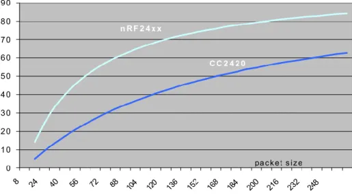
2.4.4 Nordic Semi nRF24L01
This is a single chip transceiver, operating in the 2400 to 2483.5 MHz band with GFSK modulation and an air data rate up to 2Mbps. With integrated baseband protocol engine enabling packet communication, reducing the number of link-layer functions to be implemented by the application. Although the predefined output power range (-18dBm to 0dBm) is sufficient to most applications, it is possible to couple a RF amplifier to the chip in order to achieve transmission powers above 0dBm. (12)
Figure 5 - nRF24L01 channel distribution (1Mbps mode) (11)
Being a highly integrated chip provides almost all of the necessary functions to operate. It has integrated voltage regulators that ensure a high PSRR allowing it to operate over a broad range of voltages. Also this device is able to operate from an inexpensive 60ppm 16MHz crystal which further reduces BOM costs. (12)
As referred above, this chip integrates baseband protocol engine enabling packet communications, referred as Enhanced ShockBurst™. It is a data packet link layer application, providing automatic packet assembly, timing, acknowledgement and retransmission of packets. It allows 1 to 32 byte dynamic packet size, and boasts 6 data pipe MultiCeiver™ for up to 1:6 node star networks. (8)
2.4.5 Wireless communications conclusions
The possibility to build peripherals with 802.11 standards is limited to the system capabilities, as the protocol stack is relatively complex and most implementations require the peripheral to run, at least, an embedded operating system.
Also the previous limitations of the allowable channels further impair the adoption of 802.11 as a wireless solution for this application, as it would be required that a few dozens of devices to operate in close proximity range. Such approach would increase
development cycles and costs and adding the scalability issues mentioned earlier makes 802.11 impractical to this application.
Bluetooth in the other hand aims to reduce peripheral complexity, but still require the host to be act as a master, increasing the host’s complexity, thus impairing the implementations of inter-peripheral communications as needed in a wireless datalogger. Further impairments arise from the fact that in its basic form, Bluetooth master can only communicate with 7 slaves in a given network, limiting the number of devices that could be simultaneously connected to, for example, a personal computer, and therefore limiting system scalability.
Further improvements to Bluetooth impairments regarding latencies and setup complexity are made by ZigBee, sacrificing bandwidth and profiles. One interesting aspect of ZigBee is the availability of devices operating with transmission of 20dBm or more (10), which would allow communications between two devices to the a few kilometers range, being useful for telemetry for example.
The main issue in ZigBee is that the price range of such modules does not allow a solution to be cost effective, and the higher consumption/lower bandwidth efficiency of 802.15.4 DSSS make it less attractive than simpler protocol stacks. (11)
Figure 6 - nRF24L01 vs. ZigBee communication efficiency (11)
While being a proprietary stack, the Nordic solution, the nRF24L01 chip, is the solution of choice, as it delivers the needed functionalities while keeping software complexity to a minimum. Its low power characteristics, while not being paramount in this application, are desirable as to provide high mobility for a battery powered, datalog capable module.
The high scalability provides an advantage in this application, as it is possible to operate this device in 1MHz or 2MHz bands over the 2.4GHz ISM band, allowing up to 41
non overlapping channels to be deployed in close vicinity with a resolution of 1MHz. Even with overlapping channels, the Enhanced ShockBurst™ ensures packet transmission and retrial and, at the limit, takes full advantage of the fact that each device occupies roughly the channel at 60.6% capacity (maximum 164µs air time, with 130µs interval until acknowledgement is sent with 36,5µs air time minimum), thus easily accommodating two different communication channels. (12)
This device also has the capability to transmit data on the acknowledgment packets, although packet transmission is not guaranteed, which is very suitable for bidirectional signalization algorithms, and in addition to this, the nRF24L01 is able to rapidly change frequency and perform carrier sensing (about 300µs for a complete cycle), which allows to deploy frequency hopping solutions and/or or frequency spread spectrum capabilities. (12) (13) (14)
3 Description
Summary
This section describes the cores developed in this paper. It is divided by area of research and each area is described with a top-down approach.
3.1 Mass storage
3.1.1 MMC Electrical Standard, Standard Capacity (MMCA 4.1) 3.1.1.1 Introduction
“The MMC card is a universal low cost data storage and communication media” (15).
Figure 7 - MMC card architecture (15)
Based on a ten-wire bus topology, with speeds up to 52MHz yielding a maximum throughput of 416Mbps and is able to operate either at 1-bit, 4-bit or 8-bit bus width. It also supports lower bandwidth SPI bus (100-300 kbps).
The MMC bus lines are as follows: CLK Bus clock provided by the host CMD Bidirectional command line DAT[0:7] Bidirectional data line
3.1.1.2 MMC Registers
The MMC implements 6 mandatory registers, as described below:
CID Card IDentification number, a card individual number for identification
RCA Relative Card Address, is the card system address, dynamically assigned by the host during initialization.
DSR Driver Stage Register, to configure the card’s output drivers.
CSD Card Specific Data, information about the card operation conditions.
OCR Operation Conditions Register. Used by a special broadcast command to identify the voltage type of the card.
EXT_CSD Extended Card Specific Data. Contains information about the card capabilities and selected modes. Introduced in specification v4.0
Table 2 - MMC registers
3.1.1.3 MMC Transfers
Bus transfers are defined in the bus protocol as an exchange of messages between the host controller and the card, composed by tokens. These tokens are defined as:
Command A command is a token which starts an operation. A command is sent from the host to a card. A command is transferred serially on the CMD line.
Response A response is a token which is sent from the card to the host as an answer to a previously received command. A response is transferred serially on the CMD line.
Data Data can be transferred from the card to the host or vice versa. Data is transferred via the data lines. The number of data lines used for the data transfer can be 1(DAT0), 4(DAT0-DAT3) or 8(DAT0-
DAT7).
Table 3 - MMC tokens
The MMC standard supports two types of data transfers: Sequential
commands
These commands initiate a continuous data stream; they are terminated only when a stop command follows on the CMD line. This mode reduces the command overhead to an absolute minimum. Sequential commands
are only supported in 1-bit bus mode.
Block-oriented commands
These commands send a data block followed by CRC bits. Both read and write operations allow either single or multiple block transmission. A multiple block transmission is terminated when a stop command follows on the CMD line similarly to the sequential read.
Table 4 - MMC supported transfers
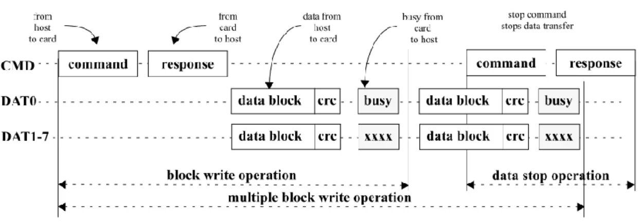
The following section describes these transfers timing diagrams. For sequential reads it is as follows:
Figure 8 - Sequential reads (15)
The block reads have a similar timing diagram:
Figure 9 - Block reads (15)
As for writes, the sequential writes are as follows:
The block write operations are defined as:
Figure 11 - Block write (15)
There are also some transfers that do not involve data transaction or even response, these transfers are as follows:
Figure 12 - No response and no data transfers (15)
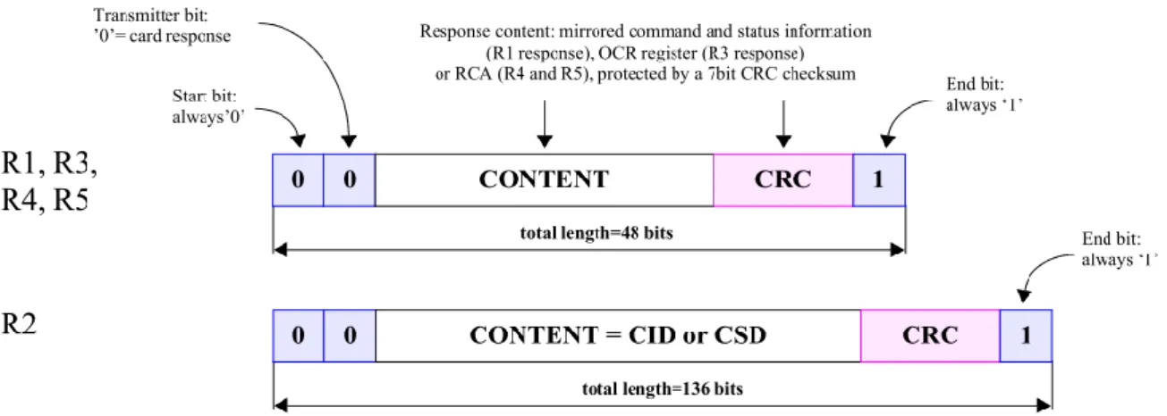
3.1.1.4 MMC Token format
All tokens transfers are CRC protected, using either CCITT CRC7 (except for R3 responses or CID and CSD registers) or CRC16. All data transfers are protected using CRC16, with the exception of sequential data access.
The MMC token format is divided in two categories, command and response. The command format is defined as:
The response token format is defined as:
All data transactions for 1-bit, 4-bit and 8-bit bus widths, regardless of the direction, are defined as follows:
3.1.2 Mass storage overview
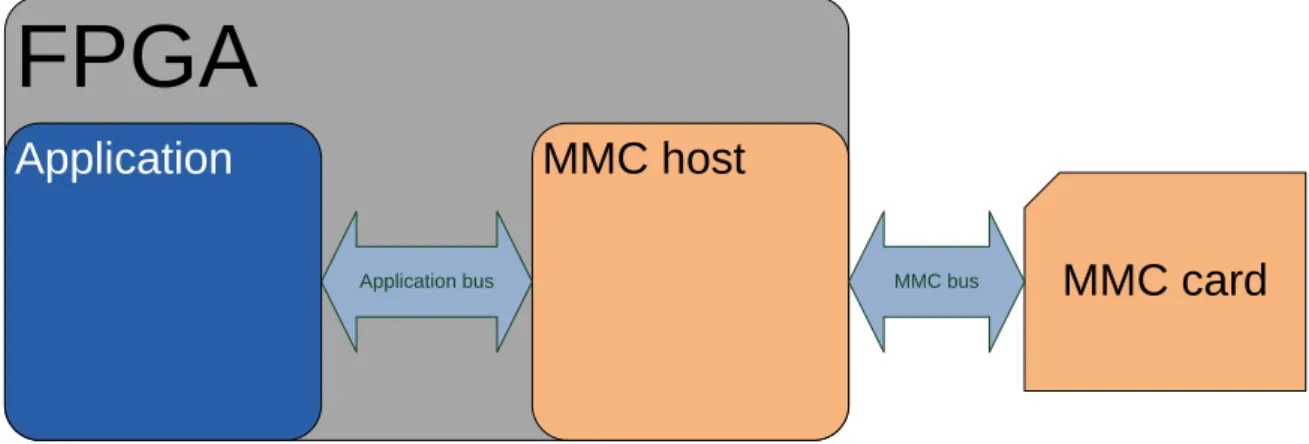
Mass storage was achieved implementing a MMC host on FPGA as follows:
FPGA
MMC card
MMC host
Application busApplication
MMC busFigure 16 - Mass storage overview
The MMC bus offered several advantages over other solutions, such as:
Availability of low cost MMC cards with more than enough performance (up to 52MBps burst bandwidth)
Reduced number of lines needed to interface the FPGA to the MMC card
Availability of documentation and application notes
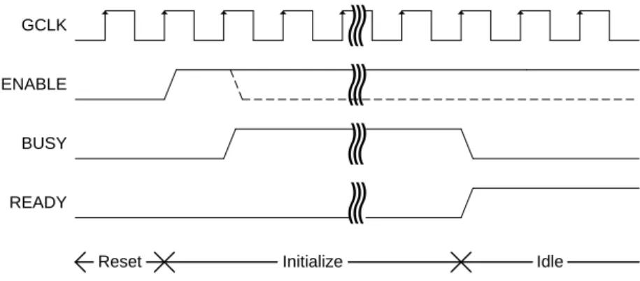
The implemented MMC host has support for 1 bit MMC communications, up to 50MHz clock rate and single block transfers. The host structure overview is illustrated on
Figure 17. MMC host Data handler Command handler MMC controller MMC block cache CMD DAT CLK
Figure 17 - MMC host overview
The MMC host has the following blocks:
MMC block cache
MMC controller
Command handler
3.1.2.1 MMC block cache
MMC block cache
Dual port RAM (BLOCK Read)
2048x8bit
Dual port RAM (BLOCK Write)
2048x8bit
Figure 18 – MMC block cache overview
The MMC block cache has a total of 4kByte of RAM and is the ECU cell interface providing direct access to the MMC sectors.
In order to interleave read and write operations, as well as allowing having concurrent process to perform read and write operations on the MMC card, the MMC block cache has two independently addressable Dual Port RAM units. This leads for increased performance as the ECU cell using the MMC host is able to interleave read and write operations, transferring data from/to one half of the cache as the other is in use by the MMC host.
Each of the Dual Port RAM units has 2kByte address space (2048x8bit), so up to 2kByte block reads/writes are allowed. 3.1.2.2 MMC controller MMC controller Idle Initialize Read block Write block Reset Success Failure Read Write
Figure 19 - MMC Controller overview
The MMC controller manages all aspects of the MMC bus such as Card Management, Card Interface Macros and MMC bus clock.
It also controls the remaining blocks of the MMC host during read or write operations.
After a system reset or power on reset, the card is initialized before usage, as the card state is unknown.
After successful initialization, the MMC controller idles until a read or write operation is requested by the ECU cell.
Any read or write operation is issued by the ECU cell to this block and the respective handshake signals are driven by this block, implementing basic handshaking to the ECU cell.
3.1.2.3 Command handler COMMAND handler CMD CRC Logic Rx Logic Tx Logic ENB Q Q SET CLR D Q QSET CLR D State machine Q Q SET CLR D Q QSET CLR D MMC Clk Q Q SET CLR D CRC7 S1 S2 D C ENB Multiplexer Q Q SET CLR D
Figure 20 – Command handler overview
The command handler implements the bus level MMC protocol such as CRC
calculation and generation, data inflation, data deflation and handshaking.
For this purpose, a small but fast finite state machine was implemented in hardware, in order to control all aspects referred above.
The advantage of this scheme is to encapsulate all of the bus level functions in one block to reduce complexity of the MMC host.
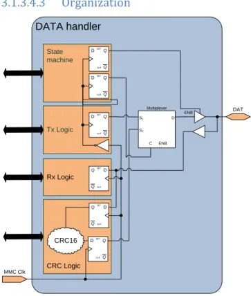
Note that the same CRC generator is used for both incoming/outgoing messages in order to reduce resource consumption. 3.1.2.4 Data handler DATA handler DAT CRC Logic Rx Logic Tx Logic ENB Q Q SET CLR D Q QSET CLR D State machine Q Q SET CLR D Q QSET CLR D MMC Clk Q Q SET CLR D CRC16 S1 S2 D C ENB Multiplexer Q Q SET CLR D
Figure 21 - Data handler overview
Data handler is similar to the command handler as the main difference is in the CRC block that is changed to match MMC specifications, and the data frames total length requires a more subtle approach for serial – parallel conversion.
Nevertheless, the similarity of the structures allows code reuse to some extent, reducing the overhead time to develop this block, maintaining the small footprint and fast responsiveness of the system.
3.1.3 Mass storage details 3.1.3.1 MMC block cache 3.1.3.1.1 Interface signals
The MMC block cache interfaces with the ECU cell with the following signals:
RD_ADDR[10:0] RDADD[10:0] RD_DOUT[7:0] RDDOUT[7:0] RDWEN WR_ADDR[10:0] WRADD[10:0] WR_DOUT[7:0] WRDOUT[7:0] WR_DIN[7:0] CLK WR_EN RDDIN[7:0]
Figure 22 - MMC block cache interface
This block’s interface signals summary is available on Table 5 - MMC block cache signals.
Signal Name Width Direction Description
RD_ADDR 11 IN Read block port a address
RD_DOUT 8 OUT Read block port a data out
RDADD 11 IN Read block port b address
RDDOUT 8 OUT Read block port b data out
RDDIN 8 IN Read block port b data in
RDWEN 1 IN Read block port b write enable
WR_ADDR 11 IN Write block port a address
WR_DOUT 8 OUT Write block port a data out
WR_DIN 8 IN Write block port a data in
WRADD 11 IN Write block port b address
WRDOUT 8 OUT Write block port b data out
CLK 1 IN Clock in
Table 5 - MMC block cache signals
The block read operations have an 11 bit address bus (RD_ADDR[10:0]) and an 8 bit width data bus (RD_DOUT[7:0]).
To access the address space reserved for write operations it’s available a 11 bit address bus (WR_ADDR[10:0]), a 8 bit data bus for write operations (WR_DIN[7:0]) and a 8 bit data bus for read operations (WR_DOUT[7:0]) along with a write enable signal (WR_EN).
The block read/write operation completion is signaled by the MMC controller, described further ahead, as such, during a block read/write operation it’s not recommended to change the contents of the write block address space as written data will be unknown, as well the read block address space should only be read after the read operation completes successfully.
3.1.3.1.2 Building blocks – the Dual Port RAM
The implementation of the MMC block cache was based on the Dual Port RAM blocks available in the Spartan 3E FPGA. This allows greater throughput, and smaller footprint than a discrete solution.
ADDRA[10:0] DINA[7:0] DOUTA[7:0] WEA 2048 x 8 CLKA ADDRB[10:0] DINB[7:0] DOUTB[7:0] WEB CLKB
Figure 23 – 2048 x 8 bit Dual Port RAM
The Spartan 3E Dual Port RAM was synthesized by using the Block Memory Generator at Xilinx® CORE Generator™ program, which is a design tool that delivers parameterized IP core optimized for Xilinx® FPGAs
Figure 24 – Xilinx ISE Block Memory Generator
ADDRA[10:0] DINA[7:0] DOUTA[7:0] WEA 2048 x 8 CLKA ADDRB[10:0] DINB[7:0] DOUTB[7:0] WEB CLKB ADDRA[10:0] DINA[7:0] DOUTA[7:0] WEA 2048 x 8 CLKA ADDRB[10:0] DINB[7:0] DOUTB[7:0] WEB CLKB RD_ADDR[10:0] RD_DOUT[7:0] WR_DOUT[7:0] WR_ADDR[10:0] WR_DIN[7:0] WR_EN RDDOUT[7:0] RDADD[10:0] RDDIN[7:0] RDWEN WRDOUT[7:0] WRADD[10:0] WR_EN
Figure 25 - MMC cache detail
As a dual-port RAM, the MMC block RAM allows both ports to simultaneously access the same memory cell. Potentially, conflicts arise under the following conditions:
1. If the clock inputs to the two ports are asynchronous, then conflicts occur if clock-to-clock setup time requirements are violated.
2. Both memory ports write different data to the same RAM location during a valid write cycle.
3. If a port uses WRITE_MODE=NO_CHANGE or WRITE_FIRST, a write to the port invalidates the read data output latches on the opposite port.
The clock domain is the same for each port, so condition 1 is not met.
In this specific application, for each memory module there’s only one process that modifies the contents of the memory cells, so the condition 2 is not met.
As the read/write operations are signaled to the ECU cell by handshaking signals, read and write operations should be mutually exclusive in read or write block address areas. This is an assumption, as the ECU cell has to guarantee that there’s no read / write collisions.
This leads to the conclusion that as long as the previous conditions are met, Dual Port RAM conflicts are not an issue in this design.
3.1.3.1.3 Signal sequence introduction
The implemented RAM is based on synchronous, positive edge triggered dual port RAM’s, so read and write operations have the following sequence:
3.1.3.1.4 Read block address space signal sequence
RD_CLK
RD_ADDR[10:0] X A B C D
RD_DOUT[7:0] X R[A] R[B] R[C] R[D]
Figure 26 - MMC block cache read timing
As it can be seen, the RD_DOUT data changes after RD_ADDR is stable during a RD_CLK positive edge, thus introducing one cycle data latency.
This is the behavior of a standard synchronous RAM.
3.1.3.1.5 Write block address space signal sequence
WR_CLK WR_ADDR[10:0] X A B C D WR_DOUT[7:0] X R[A] R[B] R[C] R[D] WR_DIN[7:0] X 0x80 0xFF 0x4F 0x28 WR_WEN A B C C 0x80 0xFF 0x4F 0x28 X
As long as WR_WEN is logical ‘0’, the block RAM behaves has seen in the read sequence, being the WR_DOUT updated with the contents of the RAM with one cycle data latency. As the WR_WEN is driven to logical ‘1’, the addressed space in the RAM is written with the data present at WR_DIN bus at the next WR_CLK positive edge.
Also, this is the behavior of a standard synchronous RAM.
3.1.3.2 MMC controller 3.1.3.2.1 Interface signals RDBLK[22:0] MCLK RDEN #MCLKEN RDBUSY RDERROR CMDEN CMDBUSY WRBLK[22:0] CMDERROR WREN CMDINDEX[5:0] WRBUSY CMDARG[31:0] WRERROR CMDDOUT[31:0] CMDADD[2:0] ENABLE BUSY DATEN DATBUSY CLK DATERROR RSTIN WRBLK RSTOUT READY MMC controller
Figure 28 - MMC controller interface signals
The MMC controller provides the interface between the ECU cell and the command and data handler. Its signals are described on Table 6 - MMC controller interface signals.
Signal Name Width Direction Description
RDBLK 23 IN MMC block to read (23 MSB of 512 byte aligned address)
RDEN 1 IN Drive logic ‘1’ for one clock cycle to start block read
RDBUSY 1 OUT Logic ‘1’ while reading
RDERROR 1 OUT Logic ‘1’ if read fails, reset at next block read
WRBLK 23 IN MMC block to write (23 MSB of 512 byte aligned address)
WREN 1 IN Drive logic ‘1’ for one clock cycle to start block write
WRBUSY 1 OUT Logic ‘1’ while writing
WRERROR 1 OUT Logic ‘1’ if write fails, reset at next block write
BUSY 1 OUT Logic ‘1’ while not in Idle state
CLK 1 IN Master clock input
RSTIN 1 IN Reset input
RSTOUT 1 OUT Reset output
READY 1 OUT Logic ‘1’ after successful initialization
MCLK 1 OUT MMC clock output
#MCLKEN 1 OUT MMC clock output tri-state buffer control
CMDEN 1 OUT Command handler enable signal
CMDBUSY 1 IN Command handler busy signal
CMDERROR 1 IN Command handler error signal
CMDINDEX 6 OUT Command index
CMDARG 32 OUT Command argument
CMDDOUT 32 IN Command response
CMDADD 3 OUT Internal register address
DATEN 1 OUT Data serializer enable signal
DATBUSY 1 IN Data serializer busy signal
DATERROR 1 IN Data serializer error signal
3.1.3.2.2 MMC card Initialization
The MMC controller block implements the control finite state machine required for card initialization after power-up or reset and transfer management at each read/write cycle.
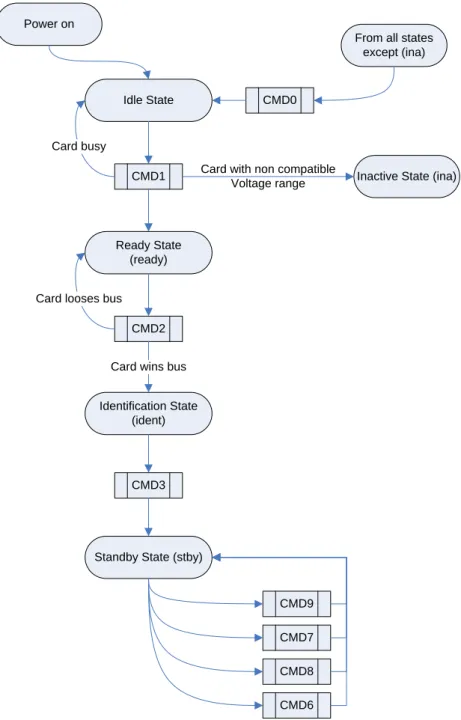
The MMC card initialization state diagram is defined as follows:
Idle State CMD0
Power on
From all states except (ina)
CMD1 Card busy
Inactive State (ina) Card with non compatible
Voltage range
Ready State (ready)
Identification State (ident)
Standby State (stby) CMD2
Card wins bus Card looses bus
CMD3
CMD9
CMD8 CMD7
CMD6
Figure 29 - MultimediaCard state diagram (card identification mode)
As the card state is unknown upon reset / power up, software reset (CMD0) is issued after a minimum of 1 millisecond of waiting time. After the software reset, the CMD1 is sent to the card, with the argument indicating that this is a high voltage card. Upon
successful completion of this command, the MMC card’s OCR register is read using CMD2, followed by the card’s CID (Card Identification Data) register readout using CMD3. As this is a single MMC card bus, the RCA (Relative Card Address) is assigned to 2 by default.
After successful initialization, the CSD (Card Specific Data) and the EXT_CSD (Extended Card Specific Data) are read from the MMC card and the card is switched to High Speed mode.
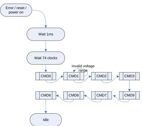
Synthesizing into a flowchart, the implemented initialization is as follows:
Wait 74 clocks CMD1 Wait 1ms CMD0 Invalid voltage range CMD2 CMD3 CMD9 CMD8 CMD7 CMD6 Error / reset / power on Idle
Figure 30 - MMC controller initialization
During initialization the CMD6 reads the EXT_CSD register from the MMC card. This register is not read as all the other registers (via CMD line), but as a data block (via DAT lines).
As such, and in order to reduce resource consumption and system complexity, the EXT_CSD register is read into the MMC Block Cache during the execution of CMD6.
This leads to if the ECU cell has the need to access the EXT_CSD data, the later is available right after initialization in the MMC Block cache lower 512 bytes address space (0x0000 – 0x01FF).
Note that the MMC block cache address space holding the EXT_CSD data is lost on the first block read operation, such data can be retrieved anytime by resetting the MMC controller, forcing the controller to re-initialize the MMC card.
3.1.3.2.3 MMC card basic operations - Block read Idle CMD17 RDEN = 1 Update flags Update flags Exit Operation not complete RDEN = 0
Figure 31 - Block Read
To start the block read sequence, the ECU cell drives the 23 MSBs of the target sector into the RDBLK bus, and asserts the RDEN signal, clearing the RDERROR bit and setting the RDBUSY bit.
Upon operation completion the RDBUSY flag is reset and the RDERROR
flag is set accordingly to the operation result.
To initiate a second transfer the RDEN bit needs to be reset for at least one clock cycle.
During this operation the block read address space at the MMC block cache is being written as the data is shifted from the MMC bus, as such it is not recommended to read it until operation completion, otherwise data is likely to be corrupted.
The block write address space at the MMC block cache can be read at any time during this operation.
3.1.3.2.4 MMC card basic operations - Block write
Idle CMD17 RDEN = 1 Update flags Update flags Exit Operation not complete RDEN = 0
Figure 32 - Block Write
To start the block write sequence, the ECU cell drives the 23 MSBs of the target sector into the WRBLK bus, and asserts the WREN signal, clearing the WRERROR bit and setting the WRBUSY bit.
Upon operation completion the WRBUSY flag is de-asserted and the WRERROR flag is set accordingly to the operation result.
To initiate a second transfer the WREN bit needs to be reset for at least one clock cycle.
During this operation the block write address space at the MMC block cache is being read as the data is shifted to the MMC bus, and it is not recommended to modify it until operation completion, otherwise data corruption is most likely to occur at the MMC card.
The block read address space at the MMC block cache can be read at any time during this operation.
3.1.3.2.5 Error handling
The MMC controller block monitors the Command and Data handler error lines, and in any error event the current operation is aborted and the error is signaled to the ECU cell.
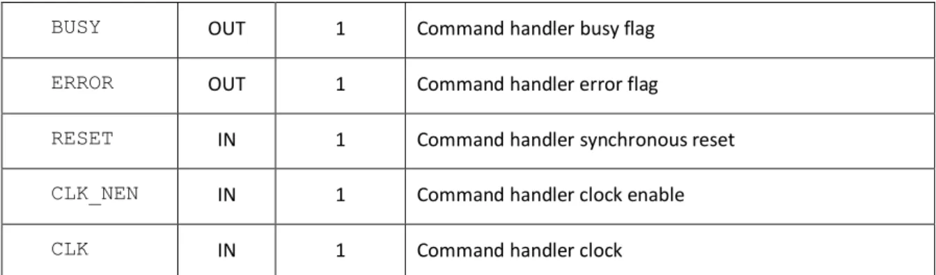
This allows for the ECU cell to decide whether to retry or to move on, based on the implemented algorithm. 3.1.3.3 Command handler 3.1.3.3.1 Interface signals CMD_INDEX[5:0] CMDIN CMD_ARG[31:0] CMDOUT CMDRX REGDOUT[31:0] REGADD[3:0] DAT0 ENABLE BUSY CLK CLK_NEN RESET ERROR
Figure 33 - Command handler interface signals
The signals available to control the Command handler are available on Table 7 - Command handler interface signals
Signal Name Width Direction Description
CMDIN IN 1 CMD line output – tie directly to IOB
CMDOUT OUT 1 CMD line input– tie directly to IOB
CMDRX OUT 1 CMD line output enable – tie directly to IOB
DAT0 IN 1 DAT0 line input – tie directly to IOB
CMD_INDEX IN 6 Command index bus
CMD_ARG IN 32 Command argument bus
REGDOUT OUT 32 Response cache data out
REGADD IN 4 Response cache address
BUSY OUT 1 Command handler busy flag
ERROR OUT 1 Command handler error flag
RESET IN 1 Command handler synchronous reset
CLK_NEN IN 1 Command handler clock enable
CLK IN 1 Command handler clock
Table 7 - Command handler interface signals
3.1.3.3.2 Organization COMMAND handler CMD CRC Logic Rx Logic Tx Logic ENB Q Q SET CLR D Q QSET CLR D State machine Q Q SET CLR D Q QSET CLR D MMC Clk Q Q SET CLR D CRC7 S1 S2 D C ENB Multiplexer Q Q SET CLR D
Figure 34 - Command handler overview
The command handler is built around two shift registers (one for incoming command frames and the other for
outgoing command frames) and a common CRC generator with serial data output for both incoming and outgoing frame transfers.
A state machine binds all the components and provides for:
- Response type and length management
- Handshaking - Error management - Card register caching
3.1.3.3.2.1 State machine
This block has the task of building the transmission frame, switching the CMD output between the transmission frame shift register and the CRC generator output accordingly, detect the response length and handshaking for any given command index, verify incoming transmissions CRC.
3.1.3.3.2.2 TX Logic
This block is a simple shift register that holds the frame built by the state machine as the command was queued, and shifts-it out to the CMD line.
As the TX Logic block, this block is a simple shift register and holds the complete received frame from the CMD line.
3.1.3.3.2.4 Response cache
This block is a 512 byte RAM used to cache the latest responses. This can be useful as the MMC host gets more complex and a broader range of MMC cards compatibility is desired. In this stage this cache can be used in order to configure the MMC parameters for optimal performance to a given MMC card.
The Response cache memory map is as follows:
Start Address Register Length (bits)
0x00 R1 32 0x01 R3 32 0x02 R2 (CMD2 or CMD10) 128 0x06 R2 (CMD9 only) 128 0x0A R4 32 0x0B R5 32
Table 8 - Response cache memory map
3.1.3.3.2.5 CRC Logic
The implemented CRC algorithm is standard CCITT-CRC7, as defined in the MMC Specification v4.1.
The CRC input is driven directly from the CMD line, so the same CRC generator can be used for both incoming and outgoing transmissions, thus reducing the logic consumption.
Figure 35 - CRC7 generator
In order to append the calculated CRC into the CMD line as the last part of the command frame being transmitted, the Command handler implements a multiplexer to the CMD line that takes the output from the Tx Logic as well the CRC generator output and is controlled by the state machine.