Journal of Engineering Science and Technology Review 8 (3) (2015) 14-20
Research Article
A Novel Approach to Synchronous Image Acquisition from Near Infrared Camera in
Optical-Surgery Navigation System
Rongqian Yang 1, Peifeng Guan 1, Ken Cai 2,*, Weihu Xiao 1, Xuan Si 1, and Zeng ZhaoFeng 3
1Department of Biomedical Engineering, South China University of Technology, Guangzhou 510006, China
2School of Information Science and Technology, Zhongkai University of Agriculture and Engineering, Guangzhou 510225, China 3Department of Mathematics and Computer Science, California State University, CA 94542, U.S.A
Received 14 February 2015; Accepted 23 October 2015
___________________________________________________________________________________________
Abstract
The positional accuracy of an optical-surgery navigation system is significantly affected by two factors. One is the acquisition synchronism of the two cameras in the system, and the other is the phase difference in image transmission acquired by these cameras. To further enhance image-acquisition synchronism, a field programmable gate array (FPGA)-based synchronous-acquisition method is introduced in this paper. The FPGA control circuit board is independently designed to equalize the length of all data lines, thereby reducing differences in image transmission. Two Complementary Metal Oxide Semiconductors (CMOS) image sensor chips of MT9V032 are also adopted to enable synchronous acquisition in passive acquisition mode. Moreover, the control of exposure time and frame number of MT9V032 under the passive acquisition mode is discussed. Finally, the proposed method is validated and the experimental results the two cameras show high synchronicity and performance in image-acquisition and have good adaptability in different circumstance.
Keywords:Optical-surgery navigation, Synchronous Acquisition, Passive sequential, Equilong
__________________________________________________________________________________________
1. Introduction
Surgery navigation systems (SNSs) [1-3] can enable accurate real-time tracking and positioning during surgery by providing the relative position and direction of surgical instruments to the nidus area for surgeons. The quality of an SNS is directly determined by its positioning technology. Optical positioning technology is presently the most widely used positioning technique because of its high accuracy and flexibility. The theory of optical positioning, which is mainly dominated by infrared optical positioning, states that through a two-camera visualization system formed by two near-infrared cameras, the images of specific marks on a target surface or in a target can be acquired. Subsequently, their surface shapes and 3D positions are re-established, and stereotaxic positioning is carried out according to the mutual relation between the coordinates of the images and the World Coordinate System. Thus, two cameras can acquire target images (i.e., acquisition synchronism of two cameras) while significantly affecting the positional accuracy of the optical navigation system. However, the phase difference in images transmission acquired by the two cameras [4, 5] may influence the accuracy of positioning and processing speed of the system.
Studies on optical positioning mainly focus on the registration of surgical instruments, camera orientation, location tracking of pinpoint, and other research on algorithm. For example, Wittmann et al. [6] proposed the
registration method of surgical instruments, which can automatically and continuously improve registration accuracy during surgeries. En Peng et al. [7] introduced the camera-calibration method by using the simple one-dimensional line segment. Cheng Yanmei et al. [8] studied the registration technique of patients and surgical robots. Huang Min et al. [9] also studied the pinpoint fully automatic tracing algorithm. Meanwhile, Shen Tong et al. [10] considered the camera calibration of a two-camera visualization system, stereo rectification, matching, and other technologies. In the aspect of hardware building of optical positioning system, the Polaris series of Canadian NDI whose positional accuracy is 0.25 mm dominate the market. However, the Polaris series is disadvantageous because of its expensive costs and complicated operation. Qi Weiming et al. [11] used a stepping motor to establish an optical tracking system. Lv Jiaguo et al. [12] studied the tracking system of surgical robots and found that these systems neglect the issue of camera synchronous acquisition because of the low position accuracy of only about 2 mm. With regard to camera synchronicity, Wen Xiaoyan et al. realized the synchronous acquisition of two cameras by using the passive mode [13] of an OV7620 imaging sensor chip through field programmable gate array (FPGA) development board, which is used to control the time series of two cameras. This approach considerably improves the synchronicity of image acquisition but fails to solve the problem of phase difference during the data transmission of images. However, the passive mode of OV7620 chip can control only the simultaneous starting of two cameras rather than their time of exposure and frame number, which has significantly decreased the expandability of the system.
______________
* E-mail address:[email protected]
ISSN: 1791-2377 © 2015 Kavala Institute of Technology. All rights reserved.
J
estr
Engineering Scienceand Technology Review
Accordingly, in the present work, all data and signal lines are designed to have equal length through the independently designed FPGA control board to decrease the influence of phase difference during image transmission. With a higher level of passive control, MT9V032 as a CMOS image sensor chip is adopted to realize the following functions based on realizing synchronous acquisition: (1) control of exposure time, which allows the optical navigation system to adapt to the light changes in various environments; and (2) control of the frame number of image acquisition to inhibit the glitter phenomenon of the fluorescent lamp.
2. FPGA control circuit design
2.1 Structural design of the control circuit
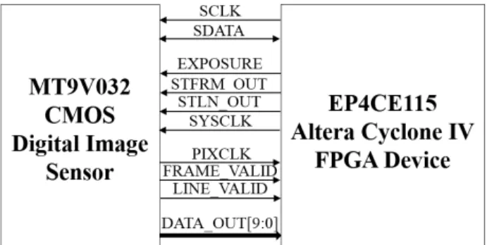
The EP4CE115 and CY7C68013 are adopted as the FPGA control chip and USB transmission controller, respectively. Two sets of IS42S16320B are used as SDRAM buffer to match the speed between USB and image collection. To realize synchronous control of two cameras, FPGA parallel processing is used to produce synchronous, control signals, to control the start of two cameras, and to upload image data through USB, which are returned by the two cameras separately passing two SDRAM buffers into the upper computer (Fig. 1).
Fig. 1. Schematic of synchronous control
2.2 Equal-length line design
The working frequencies of image collection chip, USB, and SDRAM are 27, 48, and 133 MHz, respectively, thereby comprising a high-speed circuit [14]. During the high-speed transmission of data, transport delay may occur throughout the entire process. When the lengths of signal transmission lines differ, phase difference in signal transmission may occur and cause defective signal synchronism. To address this problem, an S-shaped wiring is adopted in the circuit-board design, which ensures that the data lines are equilong and significantly reduce the phase difference during signal transmission.
Table 1. Comparison of the equal length of data lines before and after each module
Line length between FPGA and each module (unit: mil) Before equal length After equal length
FPGA and interfaces of two cameras 3440.3±160.6 3605.8±5.0
FPGA and USB controller 1389.1±423.3 1812.4±0.1
FPGA and two SDRAM buffers 1591.7±556.1 2147.8±0.2
To solve the differences of lengths of data lines, the self-designed control circuit is adopted. S-shaped wirings are adopted in each group of data lines to realize their equal length. Before equalizing the length, the length difference between some data lines exceeds 1000 mil (about 25.4 mm), which is beyond the acceptable range (Tab. 1). After equalizing the length, the length difference between data lines is within 0.1 mil, among which longer ones are within 10 mil. Moreover, an S-shaped wiring is adopted when designing the circuit of an image collection chip to minimize the phase difference in signal transmission.
3. Design of image synchronous acquisition
3.1 Sequential control of passive acquisition mode CMOS image collection chip MT9V032 is used in this paper. This chip has a high-ranking passive control mode with the highest resolution ratio of 752×640, with the highest frame number of 60 frames per second. The chip also has better photosensitive property at the near-infrared part, which can meet the requirement of infrared optical positioning together with infrared filter.
To address the issue of synchronization acquisition of cameras through FPGA, the allocation of MT9V032 internal memory is conducted under the passive collection mode. Subsequently, the synchronous collection of two cameras can be controlled by a sequence signal. Chip MT9V032 can realize the allocation of internal memory through I2C trunk. Furthermore, the synchronous control of two cameras can be
realized by exporting the synchronous control signal through the three pins (EXPOSURE, STFRM_OUT, and STLN_OUT) of MT9V032. Fig. 2 shows the circuit interconnection of FPGA and MT9V032. The third place of internal memory R0x07 of MT9V032 is set as 0 through two I2C trunks (SCLK and SDATA), thereby placing the MT9V032 chip under the passive collection mode.
Fig.2. Circuit interconnection figure between FPGA chip and MT9V032 image collection chip
Fig.3. Passive sequential control figure of MT9V032
Under the passive collection mode, the time for reading one line of the image is TR=(Width+HorBlank) ×SYSCLK. In this formula, “Width” is the window width whose value is the same as that of the internal memory R0x04 of MT9V032 (Allocation, 752), “HorBlank” is the row blank whose value is the same as that of the internal memory R0x05 of MT9V032 (Allocation, 94), and “SYSCLK” is the camera clock with 27 MHz crystal oscillator. The time for reading one frame is TF=TR×Height, where “Height” is the window height whose value is the same as that of the internal memory R0x03 of MT9V032 (Allocation, 480).
The starting and ending times of exposure are controlled by two pin signals, namely, EXPOSURE and STFRM_OUT. The exposure time TE originates from the increasing edge of EXPOSURE signal until 1 TR after the arrival of the increasing edge of STFRM_OUT signal. Moreover, TE<T 0-2×TR, where T0 is the total time of one-frame image. Thus, the exposure time can be controlled by the starting and end time of two signals, namely, EXPOSURE and STFRM_OUT, through FPGA. Moreover, the starting and end times of exposure time are linked only with the increasing edge of the two signals other than the pulse width.
Latency time TW1 is the time quantum from the end of exposure to the start of data transmission, which is decided
by the value of the internal memory R0x05 (row blank, HorBlank) and R0x06 (column blank, VerBlank) of MT9V032. Apart from representing the end of exposure phase, STFRM_OUT signal also represents the start of data reading phase. In other words, the pulse signal of STFRM_OUT may change the STFRM_OUT from the low level to the high level and trigger the readout of one-frame image. Latency time TW2= T0-(TF+TW1) is the time quantum from the finishing time of readout of one-frame image to the end of exposure of the next image. Thus, the total time of each frame image T0 must be larger than the time of readout of one image TF plus latency time TW1; otherwise, image data loss occurs.
For the pin signal of STLN_OUT, each row of image outputs 1 SYSCLK of high level to trigger the readout of each row. In other words, the pulse of 1 SYSCLK of STLN_OUT turns LINE_VALID into a high level and triggers the readout of each image row. When the pulse length of STLN_OUT turns into a high level of n SYSCLK, each n row of the image produces an output of nth row data (only one row data becomes the output, and the n–1 row(s) data of image are lost).
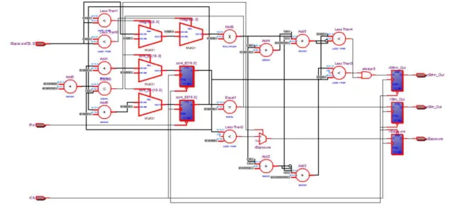
State machine causes FPGA to produce three control signals, namely, EXPOSURE, STFRM_OUT, and STLN_OUT, to realize the synchronous acquisition of two cameras; the total time of each frame image is a×TR, and the exposure time is b×TR (Fig. 4). Thus, the number of image acquisition frames and exposure time can be changed when the value of a and b is modified.
3.2 Control of exposure time under the passive acquisition mode
Under the active acquisition mode of MT9V032, the internal memory can control the exposure time through the allocation
of two I2C trunks of SCLK and SDATA. MT9V032 chip may take the new exposure time from the start of the next frame image according to the updated value. However, under the passive acquisition mode, the issue of sequential variation should be considered.
When the FPGA receives the orders of changing the exposure time from the upper computer through USB, the exposure time cannot be immediately modified. Updated exposure time should be obtained from the next frame image, such as under the active acquisition mode. Otherwise, flicker, black screen, and dislocation may appear under the following three situations (Fig. 5).
Fig.5. Control of exposure time
(1) The exposure time is reduced to A at time point B when the photosensitive element starts and continues to be exposed. Theoretically, a pulse of signal STFRM_OUT is present in the place of time point A, which shows the end of exposure, and the pulse in the place of TE disappears because of the modified exposure time. However, in this situation, the time is at point B, and the pulse of signal STFRM_OUT cannot be detected until the time point A of the next frame comes. This phenomenon causes glitter because of the prolonged exposure time. If the exposure time is lengthened at time point B, the above-mentioned problem would not occur.
(2) The exposure time is increased to D at time point C when the exposure is finished, and the image data can be read or start to be read. In this situation, the time is at time point C, and the signal STFRM_OUT's pulse at the place of TE is detected. Subsequently, the signal STFRM_OUT produces one pulse because of the modified exposure time, which shows the end of exposure, and the start of data readout occurs at time point D. Image shift occurs because of the incomplete image output. Moreover, no EXPOSURE pulse occurs to trigger the photosensitive unit between time points C and D. Thus, the data readout is zero, and the blank screen occurs. If the exposure time is reduced at time point D, the above-mentioned issues would not occur.
The above-mentioned two issues can be solved by postponing the modification of exposure time, that is, by changing the exposure time at time point 0 (the exposure start of the next frame). However, the issue of time series remains because MT9V032 chip provides a method to read out the last frame image data at the time of exposure. Afterwards, a third situation may occur.
(3) The exposure time is changed from TE to A at time point 0. In this situation, signal STFRM_OUT produces a pulse signal at time point A, which shows the end of exposure and the start of next frame image data readout. However, the last frame image data have not been completely read out at this point; thus, data are lost, and the image shifts. The exposure time can be reduced by bringing forward STFRM_OUT’s pulse, which leads to reduced readout time of the last frame image and result in image shift. Thus, to ensure sufficient readout time of the last frame image, the EXPOSURE’s pulse is postponed instead of bringing forward the STFRM_OUT’s pulse when reducing the exposure time.
Fig.6. Process of exposure time modification
3.3 Control of acquisition frame number under the passive acquisition mode
The default acquisition frame number of most image acquisition chips is 60 frames (or 30 frames), which is set due to the influence of 60 Hz power frequency in the USA to inhibit the stroboscopic phenomenon of fluorescent lamp. The theory is simple; if the power frequency is 60 Hz indoor, the lamp would flicker at 60 Hz, which is called stroboflash[15]. This kind of flicker has a fast frequency, which the naked eyes cannot realize (a human’s naked eyes cannot realize flickers with more than 50 Hz frequency) ; hence, the power frequency is set above 50 Hz. However, if the image collection chip does not collect at 60 Hz fluorescent lamp, image brightness would flicker with less than 50 Hz frequency, which can be recognized by the naked eyes. Thus, most of the image acquisition chips are set at the default frames as 60 frames (or 30 frames). The fluorescent lamp brightness becomes the same as that of the last acquisition at each acquisition to inhibit the variation in image brightness.
In some countries such as China, 50 Hz is regarded as the power frequency. Therefore, we need to reallocate the acquisition frame numbers of MT9V032 to inhibit the glitter phenomenon. Under the active acquisition mode, acquisition frame numbers can be set by allocating the internal memory of MT9V032. Nevertheless, under the passive acquisition mode, the corresponding number of rows (factor a) in one-frame time under the rate of 50 one-frames per second should be calculated:
(Width HorBlank) SYSCLK
= + ×
R
T (1)
0=a× R
T T (2)
The integer value of factor a can be obtained, that is, a=638, when the actual number is used in the formula as T0=1/50, SYSCLK=1/27000000, Width=752, and Horblank=94. The exposure time is assumed at 80 TR (b=80); hence, the state machine in Fig. 4 can be used to produce three control signals, namely, EXPOSURE, STFRM_OUT, and STLN_OUT. Subsequently, 50 frames image output can be realized under the passive collection mode.
4. Result and analysis
Fig.7. Simulation figure of a time series. (a) Each STLN_OUT pulse occupies a system clock; a row of image corresponds to one STLN_OUT pulse. (b) The exposure time is from the increasing edge of oExposure to the next row of the increasing edge of oStfrm_Out; the total time of one-frame image is the time between the rising edges of two oExposure
Fig.8. RTL circuit diagram of FPGA sequential control module
Table 2. Resource utilization table of FPGA chip EP4CE115
Total logic elements Total registers Total pins Total memory bits Embedded Multiplier 9-bit elements Total PLLs
2544 (2%) 1337 180 (64%) 30 720 (<1%) 16 (3%) 2 (50%)
4.1 Synchronicity analysis of cameras
MT9V032 chip provides an output pin named as LED_OUT. The chip has a high level under exposure, and a low one otherwise. By judging the synchronism of high and low level of its pin, we can determine whether two image acquisition chips can simultaneously carry out image acquisition. Fig. 9 shows the LED_OUT signals of two MT9V032 acquisition chips, which are obtained by the oscilloscope. Two acquisition chips have very high synchronicity, which can meet the demands of synchronous acquisition.
Fig.9. LED_OUT signals of two cameras
4.2 Stroboscopic effect analysis
To analyze the influence of acquisition frame number on the image brightness, the following experiment is conducted.
Two cameras are used to collect the static images, gain the gray value of the image under different collection frame numbers, and produce the corresponding curve of gray scale change. Fig. 10 shows the image, which is collected by the two cameras, when the collection frame number is 50 under the 50 Hz power frequency. At this time, the image does not glitter, and the grayness curve is a straight line. Tab. 3 is the curve table of gray value variation under the same image and different collection frame numbers. When the collection frame number approaches the 50 Hz power frequency, the gray curve tends to be straight. Thus, the collection frequency of 50 Hz can effectively inhibit the glitter phenomenon of lamps.
Fig.10. Fifty frame images and their gray variation curve
Table 3. The curve table of gray value variation under the same image and different collection frame number Collection frame number Waveform of gray value variation (duration of collection: 5 s)
52 frames
51 frames
50 frames
49 frames
48 frames
40 frames
5 Conclusion
The passive acquisition mode of image collection chip is adopted in this paper to realize the synchronous control of two MT9V032 image collection chips. FPGA control circuit board is independently designed to make all data lines equal in length, which further enhances the synchronism of image acquisition. Based on the passive control mode, the exposure time and frame number of two image acquisition chips can be controlled, and the acquisition performance is further enhanced. Test results show remarkable image-acquisition performance. Under the control of three FPGA signals, namely, EXPOSURE, STFRM_OUT, and STLN_OUT, the synchronous acquisition of two cameras can be realized, and the exposure time can be controlled. Moreover, the acquisition frame number is fixed at 50 by sequential control. The glitter phenomenon of fluorescent lamp is prevented, and the system acquire improved imaging performance.
Therefore, this system can effectively solve a number of problems for the optical navigation system in the image-acquisition process.
Acknowledgements
This research was funded by the Guangdong Natural Science Foundation under Grant No.S2013040014993, the State Scholarship Fund under Grant CSC NO.201408440326, the Pearl River S&T Nova Program of Guangzhou under Grant No.2014J2200049 and No.201506010035, the Guangdong Provincial Science and Technology Program under Grant No.2013B090600057 and No.2014A020215006, the Fundamental Research Funds for the Central Universities under Grant No.2014ZG003D.
______________________________ References
1. Davies, B., "A review of robotics in surgery." Proceedings of the Institution of Mechanical Engineers, Part H: Journal of Engineering in Medicine, 214 (1), 2000, pp. 129-140.
2. Peterhans, M., Oliveira, T., Banz, V., Candinas, D., Weber, S., “Computer-assisted liver surgery: Clinical applications and technological trends”, Critical Reviews in Biomedical Engineering, 40 (3), 2012, pp. 199-220.
3. Yang, R., Wang, Z., Liu, S., Wu, X., “Design of an accurate near infrared optical tracking system in surgical navigation”, Journal of Lightwave Technology, 31 (2), 2013, pp. 223-231.
4. Zhao, J., Yu, S., Cai, H., “A precise method for correcting stereo pairs collected by a new binocular device”, Industrial Robot, 34 (6), 2007, pp. 512-519.
5. Cai, K., Yang, R., Ning, H., Ou, S., Zeng Z., “An automatic algorithm for distinguishing optical navigation markers used during surgery”, DYNA, 90(2), 2015, pp. 203-209.
6. Wittmann, W., Wenger, T., Zaminer, B., Lueth T. C., “Automatic Correction of Registration Errors in Surgical Navigation Systems”, IEEE Transactions on Biomedical Engineering, 58(10), 2011, pp. 2922-2930.
7. Peng, En., Li, L., “Camera calibration using one-dimensional information and its applications in both controlled and uncontrolled environments”, Pattern Recognition, 43(3), 2010, pp. 1188-1198.
8. Chen, Y., Yang, Z., Jiang, S., “Registration technique of robot-aided image guided surgery”, Journal of Computer-Aided Design and Computer Graphics, 27(5), 2015, pp. 953-960.
9. Huang, M., Bao, S., Qiu, W., “Study and simulation of surgical navigation based on binocular vision under visible light”, Robot, 36 (4), 2014, pp. 461-468,476.
10. Shen, T., Liu, W., Wang, J., “Distance Measurement System Based on Binocular Stereo Vision”, Electronic Measurement Technology, 38(4), 2015, pp. 52-54.
11. Qi, W., Zhou, J., Zhang, X., “Optical Orientating and Tracking System Based on Nios II”, ournal of Jianghan University(Natural Science Edition), 41(2), 2013, pp. 18-22.
12. Lv, J., Jiang, X., Zhang P., “Hardware Design and Implementation of Binocular Vision System for a Medical Robot”, Chinese Optics, 7(2), 2014, pp. 307-314.
13. Wen, X., Yang, R., Wu, X., Huang, Y., “Synchronous Image Acquisition of Binocular Stereo Vision System Based on FPGA”, Video Engineering,37(5), 2013, pp. 56-59.
14. Deng, P., Wang, W., Zhang, J., “Signal Integrity Design Based on High Speed Digital Processing Module”, eronautical Computing Technique, 40(2), 2010, pp. 101-104.