Esitetyissä vuoissa yhdistyvät TTA Based Co-design Environment (TCE) -työkalupakin käyttö Kactus2 IP-XACT -suunnitteluympäristöön. Ehdotetuissa työnkuluissa yhdistyvät Co-design Environmentin (TCE) TTA-pohjainen työkalusarja ja Kactus2 IP-XACT -suunnitteluympäristö.
TCE Overview
Principles of a TTA processor
In [10] a performance comparison has been made between a simple TTA processor and different softcore processors for different applications. The TTA processor implemented with the TCE tools and the soft core processors (NIOS II/f and two MicroBlaze configurations) were synthesized and ran on FPGA.
![Figure 3: A sample TTA processor architecture [21, p. 11].](https://thumb-eu.123doks.com/thumbv2/9pdfco/1890851.267017/15.892.171.807.145.633/figure-sample-tta-processor-architecture.webp)
TCE tools
The Automatic Design Space Explorer (Explore) tool can be used to partially automate this iterative process. Other TCE tools include the Operation Set Abstraction Layer Editor (OSEd) which can be used to add information on various custom operations that FUs can perform on the relevant database.
Kactus2 overview
The IP-XACT/IEEE1685 Standard
The final configured IP-XACT design can be seen as "instructions" on how to create an executable file. All VLNV tuples are unique, independent of the type of IP-XACT object they identify.
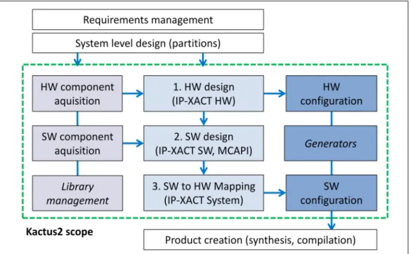
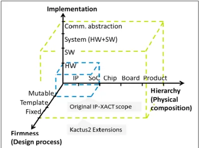
Kactus2 IP-XACT extensions
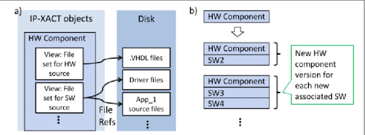
A standard IP-XACT HW component can include references to SW through model views and filesets that point to files on disk. To instantiate HW and SW components in the same IP-XACT design, a system design is defined. Since IP-XACT does not specify HW/SW mappings, a template parameter is added to each SW component for the mapping that is configured in the system design (Figure 13).
IP-XACT standard objects New Kactus2 objects HW component, HW design SW component, SW design HW design configuration API definition* (SW).
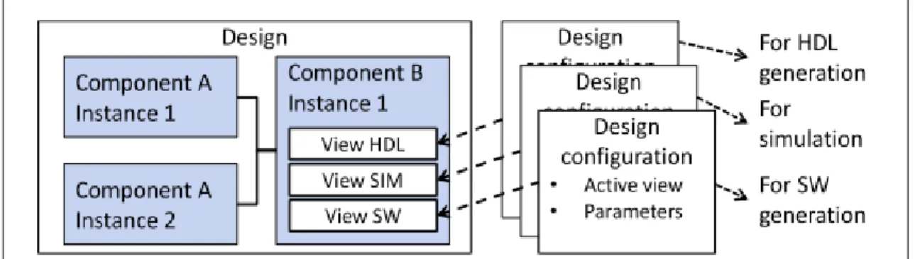
About instance management in IP-XACT
Creating a new IP-XACT component from a template or draft
The necessary interface types are automatically recognized and serve as part of the requirements for the IP development team. In the worst case, however, the library contains as many components as instances in different designs.
Completing instance-specific data into IP-XACT design
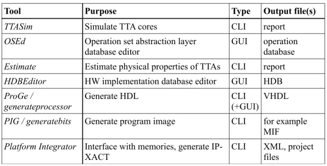
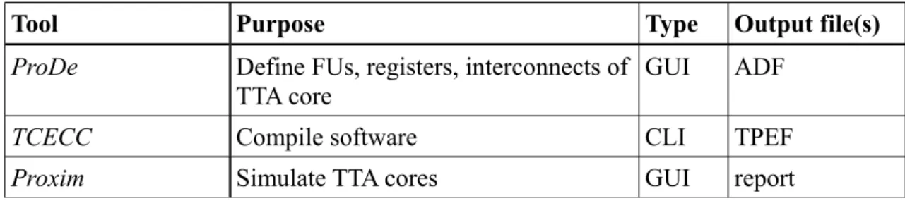
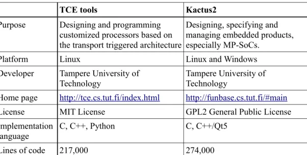
Summary of the Tools
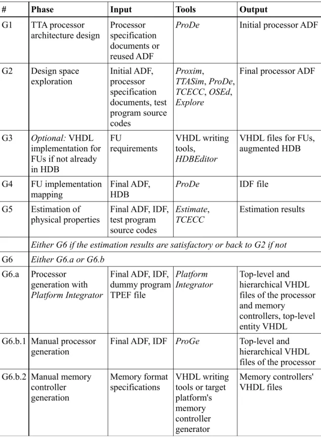
These can be stored in the IP-XACT library and the integrator can drag and drop them into an SoC design like any other IP component. The metadata of the IP-XACT processor component includes the VHDL source files for the HW and SW source code and the memory image maps of the program it executes. Evaluation of evaluation results Either F9 if the evaluation results are satisfactory or return to F4 if not F9 Either F9.a or F9.b.
Final ADF, IDF ProGe Top level and hierarchical VHDL files of the processor F9.b.2 Manual memory.
IP block design
If the Platform Integrator can be used, the final stages of the processor generation are quite easy. The ADF and IDF files are given as parameters and the VHDL implementation of the processor is saved by the tool in the target directory. The Platform Integrator has an option that automatically generates the processor's IP-XACT file.
The user adds the relevant files (VHDL, program code, documentation, and so on) to the file sets and writes a description of the component in the corresponding field.
SoC design
The generated component is stored in the IP-XACT library for integration and use in designs. Therefore, in the library is an IP-XACT component which includes a CPU element, but not a fixed program image. Many of the stages are similar to those in the previous chapter, so they are not explained in as much detail here.
Final ADF, IDF ProGe Top Level and Hierarchical Processor VHDL Files G6.b.2 Manual Memory.
Processor design
In either case, whether you use Platform Integrator or not, this stage locks the memory type format, which should be mentioned in the processor documentation. A list of all the points that should be mentioned in the processor documentation is shown here for reference. The final step in the processor design part of the flow is to create its IP-XACT description.
When using the component creation wizard, all the files related to the processor's implementation and documentation are added to the filesets by the user, and their IP-XACT description is otherwise automatically created from the top-level VHDL file.
SoC design
The designer then adds the memory image files to the filesets in the system design. All the files needed for FPGA synthesis and programming are now in the library. The TTA instances in the SoC design are replaced with those found in exploration.
In this use case, the design considerations are largely the same as in the previous chapter.
Template processor design
The address space depends on the design where the component is instantiated, so dummy values can be used here. Finally, the user defines a CPU for the component and references the address space in it. The component is then stored in the library for use and customization as an ASIP.
ASIP and SoC design
Otherwise, the memory controllers and the top-level VHDL of the TTAs must be created manually. The implementation files are stored in the filesets of the TTA component created for the design. The top-level VHDL file of the HW design can now be created using the Kactus2 VHDL generation tool along with Quartus II project files, if applicable, using the Kactus2 project file generator.
The design presented is quite simple to keep the focus on the flow instead of the intricacies of the design.
Template component creation
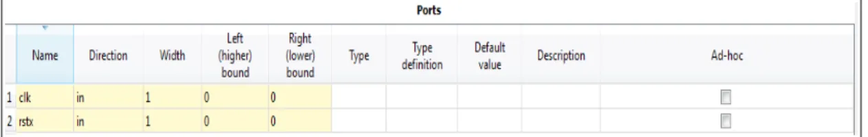
A simple TTA processor template with custom FUs enabling real-time clocking and printing to standard output is first created in the IP-XACT library. The IP-XACT file of the component is now in the library under the folder indicated by the VLNV values, but it requires further editing. The physical clock port is mapped to the bus interface in the "Port Maps" tab.
Finally, a short description of the processor for the user is written in the component description field.
Using the component in a SoC design
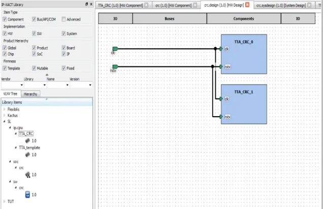
TTA, and is stored in the library as a SW component (SL/sw/crc/1.0) with the source code files in filesets. Each set of TTA files is also added at this point to the component so that they can be referenced in views. In the Kactus2 HW model, instance names are associated with corresponding views.
These are stored in the TTA component filesets in the library, with a separate fileset for each processor instance in the design.
TTA as a fixed accelerator IP block
Based on that, an estimate of the time taken by each phase in the design flows was formed. Phases F7 to F11 consist of creating the processor IP block from the source files generated in the previous steps. Taken together, phases F1 to F11, which consist of the creation of the TTA IP block, take little more than one hour in the best case where the SW application is ready in the library, no custom FUs are added in the design space exploration and Platform Integrator can be used.
It should take less than an hour, even for relatively large designs, provided everything is ready in the library.
TTA as a general purpose processor
On the other hand, while using a GPP will take less time, it will suffer from the problems of using more area, performing worse and consuming more energy. Integrating the TTA IP block into SoC designs is effortless using Kactus2 (phases F12-F15). FPGA synthesis and programming can take anywhere from a few minutes to hours, depending on the target platform and size of the design.
System design of SoC G13 1 to 10 minutes per processor depending on the complexity of the SW and MCAPI channels.
TTA as an ASIP
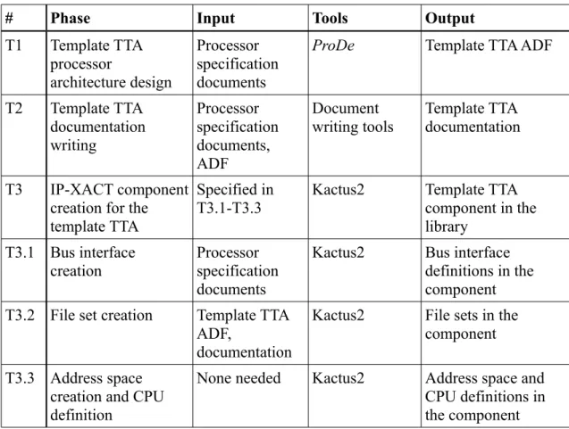
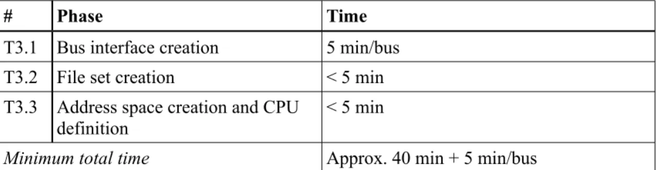
Phase Time T3.1 Creation of bus interface 5 min/bus T3.2 Creation of file set < 5 min. T3.3 Creation of address space and CPU. A6 C-code modification for TTA < 5 min to 1 hour per processor instance depending on the size of the source code and the amount of custom FU usage. The time required to design an SoC using template TTAs depends on the number of TTA instances and whether they use the same or different final processor architecture and FU implementations.
Compared to the previous use case, the ASIP approach puts more design burden on the shoulders of the SoC designer, since he also creates the internal implementation of the processors, but the end result is better optimized for the applications.
General remarks
The design flows presented reduce design time, reduce error-prone tasks, and provide product data management capabilities throughout the entire product lifecycle. For example, without an integrated design flow, the SW code running on a TTA would be "just files on disk", whereas now they can be stored in the IP-XACT library, described with metadata, and uniquely referenced from other designs . Moreover, for more complex applications, an ASIC approach is not even feasible in most cases.
On the other hand, it was found that while using a traditional GPP would save somewhat in design effort, the TTA approach enables a more efficient design with improved performance and reduced area and energy consumption, while avoiding license fees.
Suggestions for future development of the tools
Suggested modifications to the TCE tools
A file set containing the ADF and IDF files and the processor VHDL files must be added to the IP-XACT description. Of course it is impracticable to add support for every existing platform, so a good solution would be a configurable Platform Integrator where one can enter platform dependent key parameters with a graphical user interface.
Suggested modifications to Kactus2
With these additions to Kactus2, there would be little need to explicitly invoke TCE tools from the user, and most of the design flow could be operated from within the Kactus2 environment. The notable exception is the space exploration design tools, which are often used in an iterative fashion and involve several different programs than the TCE tools, and thus are more naturally used outside of the context of Kactus2. It should also be noted that Kactus2 must be running on Linux when calling the TCE tools from it as the TCE tools do not support the Windows operating system.
KAC-TUS2: IP-XACT/IEEE1685-compatible design environment for embedded Multiprocessor System-on-Chip products.