For help in crystallizing the latest topic – nanowires – in the dissertation that you – the reader – are currently browsing, I also have to thank Doctor Teppo Hakkarainen, Doctor Mikael Mulot, Doctor Hua Jiang and Professor Esko Kauppinen. In this thesis, the self-assembled vapor-liquid-solid growth of InP nanowires is studied.
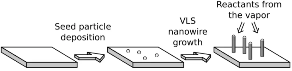
Vapor-liquid-solid growth
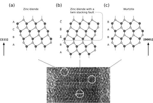
Patterning, on the other hand, can be done using, for example, nanosphere lithography [30, 31], electron beam lithography and lift-off [32], or nanoimprint lithography [33]. A crystal structure of zinc mixture can be considered as a stacked series of three different diatomic layers in the h111i direction: ABCABCABC.

Catalyst-free nanowire growth
In the absence of an In–P eutectic alloy, the liquidus line starts from the melting point of indium (157 ◦C), denoted by TIn, and increases monotonically to the melting point of InP (1071 ◦C), denoted by TInP. On the other hand, if the indium supply is greater than that required for InP precipitation, phosphorus may dissolve from the solid InP phase and indium aggregates in the droplet.
Other growth mechanisms
As more phosphorus is introduced into the liquid droplet from the vapor phase, the phosphorus concentration is momentarily higher than the equilibrium value and a solid InP phase is precipitated at the liquid-solid interface. However, for each precipitated phosphorus atom, one indium atom from the liquid is also incorporated into the lattice. A constant supersaturation, i.e. a phosphorus concentration Cs > Cg, is maintained in the In-P liquid when the consumption of indium and phosphorus in the precipitate of solid InP is balanced by the supply directly from the gas phase and possibly by surface diffusion.
If the indium supply is inadequate, the phosphorus concentration of the entire system increases continuously and, again, the droplet is eventually consumed during nanowire growth. Another effect to take into account is that there is a concentration gradient in the liquid depending on the rate of phosphorus adsorption, precipitation and diffusion. The highest concentration is at the vapor-liquid interface, and at the liquid-solid interface the supersaturation is virtually zero.
During growth, a semi-liquid SiOxlayer acts as a sink for silicon atoms in a similar way than the liquid droplet in VLS growth.
Nanowire devices and applications
The shell is a drawback of the method along with a wide diameter distribution of resulting nanowires. If precise contact of individual nanowires is not required, the statistical nature of the Langmuir-Blodgett films can be exploited for simplified and easily scalable contact [88]. This section provides a brief overview of nanowire fabrication and characterization methods used in this work.
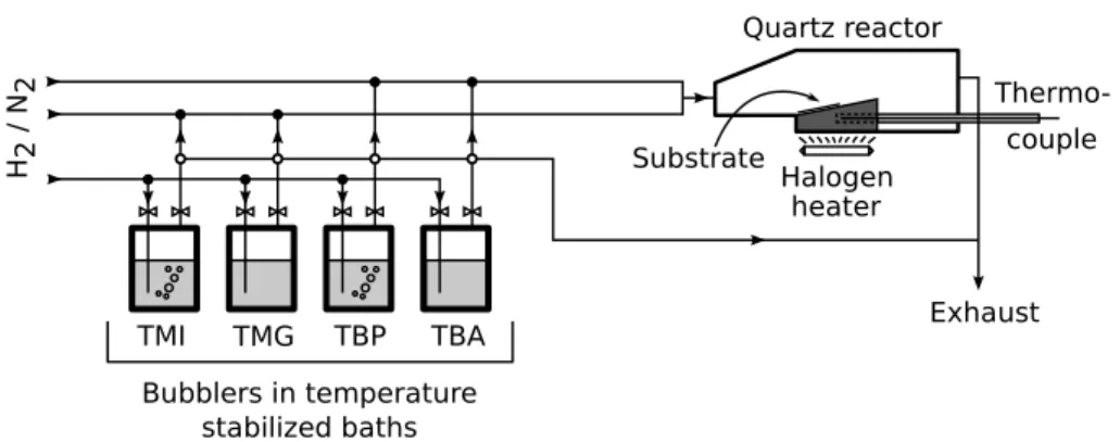
In epitaxial semiconductor growth techniques, the lattice structure of the underlying crystal, such as a substrate, is replicated in the growing layer – ideally. In metal-organic vapor phase epitaxy (MOVPE), the constituent atoms of the layer are supplied by metal-organic precursor vapors. A schematic representation of the MOVPE system used in this work for sample fabrication is shown in Fig.
However, if the true chemical catalytic action of metal nanoparticle catalysts is to be expected, the decomposition temperature of organometallic molecules can be significantly lower [12].
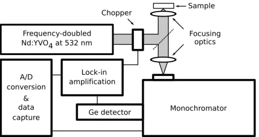
Optical characterization
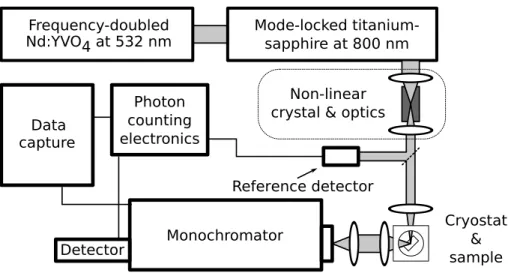
At a typical growth temperature for catalyst-free InP nanowires, 350◦C, the decomposition efficiency of TMI is highly dependent on temperature and most of the TBP molecules do not decompose at all [89]. To obtain better excitation light absorption in the InP nanowires, the pulses at the output of the mode-locked laser were frequency-doubled to 400 nm using an optically nonlinear bismuth triborate (BIBO) crystal. The pulse repetition rate of the titanium-sapphire laser was 76 MHz, estimated pulse width a few hundred femtoseconds, and the average excitation intensity of the second harmonic at the sample 10 Wcm-2.
Since the PL intensity of the grown nanowires may be low due to possible surface recombination effects, or the fact that their areal density is low, the difference of the PL signal of the nanowires from the PL signal of the substrate may be difficult. In this work the problem was solved by simply detaching the nanowires from the substrate using adhesive tape. Although the signal from the nanowires is visible even when measured on the substrate, removing the nanowires from the substrate makes the spectrum clearer and enables, e.g., peak width analysis without peak fitting.
Furthermore, it would be virtually impossible to measure TRPL from nanowires on the substrate, as at a given wavelength there would be a contribution from both the nanowires and the substrate.
Electron microscopy
The sample is illuminated using a high-energy electron beam through an electromagnetic condenser lens array. An image of the sample is formed on a fluorescent screen and can be recorded with CCD cameras. Depending on the material, the electron beam can damage the sample when imaging a small area, i.e., using high magnifications in the SEM.
This is clearly seen in the series of close-up images of a single InP nanowire grown without catalyst on InP in Figure 3.6, where the shape of the nanowire changes significantly in 40 s of continuous imaging at 300000x magnification using a beam current of about 20 nA. The surface of the nanowire turns into nanocrystalline InP, which prevents a closer inspection of the crystal structure and deflection from the core of the nanowire. The missing indium droplet at the tip is due to surface treatment of the nanowire in hydrofluoric acid and not due to beam damage as shown in Figure 2.
The susceptibility of an individual nanowire to bundle damage may depend on the local deformation or defect structure [90].

X-ray diffraction
First, the growth temperature dependence of the diameter of droplets and resulting nanowires was studied. Nanowire each type is represented by arrows in one of the SEM images in Fig. The nanowire diameter was measured at the base to enable nanowire and droplet diameter comparison and to get rid of the error due to taper.
Depending on the net flow of indium into the droplet, its diameter increases or decreases during growth, resulting in the tapering of the nanowires [54] and possibly ultimately the extinction of the droplet. Furthermore, the Gibbs-Thomson law [29] sets the lower limit for the diameter of the liquid indium droplet. With decreasing diameters the effective vapor pressure of the droplet material increases, and below the critical diameter it is higher than the partial pressure of indium in the vapor phase of the precursor and the droplet evaporates.
A comparison of the surface densities of nanowires of different types as a function of growth time is shown in Figure 1.

Nanowire growth on silicon
54, InP nanowires up to several micrometers long were grown at similar temperatures with the catalyst-free method, apparently without any kinking. The use of the catalyst-free VLS process to produce InP nanowires on silicon was studied in publication II. No nanowire growth was observed on substrates etched in hydrofluoric acid and annealed under hydrogen before growth, a result similar to a previous report on silicon nanowire growth without catalytic particles [96].
SEM images of indium droplets and droplet-seeded InP nanowires on (111) Si substrate are shown in Fig. The initial nanowire growth near the substrate surface has no clear direction and, therefore, growth is not epitaxial. The non-epitaxial growth on Si substrate with native oxide is consistent with reports on III-V nanowire growth on silicon using gold nanoparticle catalysts [15, 97].
As shown in publications I and II, catalyst-free VLS growth of size-controlled InP nanowires on InP and Si substrates using in situ deposited indium is possible.
![Figure 4.6: SEM image of (a) indium droplets and (b) InP nanowires on (111) Si. The scale bars correspond to 1 µm [publication II].](https://thumb-eu.123doks.com/thumbv2/9pdfco/19362647.0/34.892.292.651.146.526/figure-image-indium-droplets-nanowires-scale-correspond-publication.webp)
Crystal structure of catalyst-free-grown nanowires
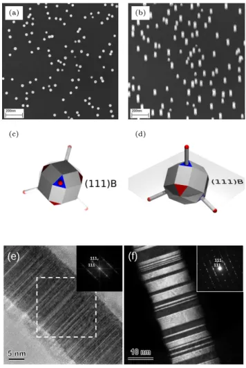
The direction of nanowire growth relative to the atomic planes of the zinc blende lattice is illustrated by a polyhedron bounded by planes with a low lattice index (Miller cube). By comparing the number of different azimuthal growth directions and the elevation angle of the nanowires and again assuming epitaxial growth, it was found that the growth direction of the nanowires was h111iB regardless of the substrate orientation on (111)A and (110) substrates. Interestingly, some indirect evidence of the initial growth of nanowires in the [111]A direction on the (111)A substrate was discovered by examining in more detail the number of different azimuthal nanowire growth directions.
This has been suggested to be explained by the initial growth of the nanowires perpendicular to the substrate surface in the [111]A direction and the formation of a 60◦ or 180◦ bifold fault before twisting into one of the energetically favorable h111iB directions. There is also clear evidence of edge faceting with bifold fault periodicity. This may be due to the instability of the substrate surface during the droplet deposition step and the formation of efficient indium sinks by surface faceting.
4.13(b) which shows that the crystalline structure is wurtzite and that the c-axis of the lattice is perpendicular to the nanowire axis.
Nanowire photoluminescence
Furthermore, it has been suggested that spectral shifts originate from Fermi level pinning in doped InP nanowires [104]. Photoluminescence spectra measured from as-grown and HF acid-treated InP nanowires are shown in Fig. PL decay curves measured from HF-treated and as-grown InP nanowires are shown in Fig.
However, the lack of blue shift may be due to the different crystalline orientation of the nanowires – with the c-axis being perpendicular to the axis of the nanowires – which has been shown to influence the PL properties of hexagonal GaN nanowires through surface effects [115]. The dotted curve shows a spectrum measured from catalyst-free grown homoepitaxial InP nanowires [publication II]. Compared with InP nanowires prepared using the catalyst-free method, one clear difference can be observed.
The average growth rate was about 24 nm/s, which is about ten times faster than the growth rate of catalyst-free homoepitaxial InP nanowires at 350 ◦C and about the same as the catalyst-free growth rate observed on silicon.
![Figure 4.14: Photoluminescence spectra of as-grown and HF acid treated InP nanowires measured at (a) 9 K and (b) 293 K [publication IV].](https://thumb-eu.123doks.com/thumbv2/9pdfco/19362647.0/41.892.186.699.147.494/figure-photoluminescence-spectra-grown-treated-nanowires-measured-publication.webp)
Photoluminescence and crystal structure
In the work presented in this thesis, the production of InP nanowires using metal-organic vapor phase epitaxy was investigated. The studies presented here mainly concentrated on a new catalyst-free method using in situ deposited indium droplets as seeds for the growth of nanowires. Homoepitaxial catalyst-free-grown InP nanowires were successfully fabricated on differently oriented substrates with typical diameters of about 20-30 nm, lengths of a few hundred nanometers, and areal densities of about 109 cm-2.
A significant increase in photoluminescence intensity was observed after hydrofluoric acid treatment of the nanowires. The unorthodox crystalline structure of nanowires grown on silicon was reflected in the photoluminescence spectra as a missing blue shift. Based on x-ray diffraction analysis, it was proposed that the blue shift was caused by nanowire crystallization in the wurtzite structure.
Different doping solubilities in the liquid phase may put some limitations on the abruptness of p-n junctions and heterointerfaces in catalyst-free fabrication.