HAL Id: tel-00768559
https://tel.archives-ouvertes.fr/tel-00768559v1
Submitted on 21 Dec 2012 (v1), last revised 5 Sep 2013 (v2)
HAL is a multi-disciplinary open access archive for the deposit and dissemination of sci- entific research documents, whether they are pub- lished or not. The documents may come from teaching and research institutions in France or abroad, or from public or private research centers.
L’archive ouverte pluridisciplinaire HAL, est destinée au dépôt et à la diffusion de documents scientifiques de niveau recherche, publiés ou non, émanant des établissements d’enseignement et de recherche français ou étrangers, des laboratoires publics ou privés.
Development of a test bench for characterization of integrated antennas at millimeter-wave frequencies
Yan Fu
To cite this version:
Yan Fu. Development of a test bench for characterization of integrated antennas at millimeter-wave frequencies. Electromagnetism. Université de Grenoble, 2012. English. �tel-00768559v1�
THÈSE
Pour obtenir le grade de
DOCTEUR DE L’UNIVERSITÉ DE GRENOBLE
Spécialité : Optique et radiofréquence
Arrêté ministériel : 7 août 2006
Présentée par
Yan FU
Thèse dirigée par Fabien NDAGIJIMANA codirigée par Laurent DUSSOPT et co-encadrée par Tan - Phu VUONG
préparée au sein du Laboratoire IMEP-LAHC dans l'École Doctorale EEATS
Development of a test bench for characterization of
integrated antennas at
millimeter-wave frequencies
Thèse soutenue publiquement le 18 juillet 2012, devant le jury composé de :
M. Mohamed HIMDI
Professeur, Ecole Supérieure d’Ingénieurs de Rennes, Président
M. Cyril LUXEY
Professeur, Université de Nice Sophia-Antipolis, Rapporteur
M. Moncef KADI
Enseignant-chercheur, ESIGELEC/IERSEEM, Rapporteur
M. Romain PILARD
Ingénieur, ST Microelectronics, invité
M. Fabien NDAGIJIMANA
Professeur, Université Joseph Fourier, Directeur de thèse
M. Laurent DUSSOPT
Ingénieur, CEA/LETI, Co-directeur de thèse
Acknowledgement
I would like to express my deep and sincere gratitude to my supervisors, Professor Fabien Ndagijimana at IMEP-LAHC and Laurent Dussopt at CEA-LETI, for their patient guidance and inspiration. Their profound knowledge and enthusiasm repeatedly helped me to overcome the unexpected-yet-inevitable difficulties that I encountered during my thesis. Working with them is also a pleasure thanks to their great sense of humor. Likewise, I express my great appreciation to my co-supervisor Tan-Phu Vuong at IMEP-LAHC for his scientific support during this thesis.
I thank Professor Mohamed Himdi from the Ecole Supérieure d’Ingénieurs de Rennes, Professor Cyril Luxey from the Université de Nice Sophia-Antipolis, Professor Moncef Kadi from ESIGELEC/IERSEEM and Romain Pilard from ST Microelectronics for kindly accepting to be my reviewers and jury members for this thesis and for their interesting questions and discussions during the defense.
I am also extremely grateful to the all the people at the IMEP-LAHC Laboratory for their help, particularly Nicolas Corrao, for being permanently available to re-calibrate the apparatus. Furthermore, I would thank to Irene Pheng at CIME Nanotech, for her dedication in realizing the flip-chip connection.
I would also like to thank to my friends, Alina Ungureanu, Leonce Mutwewingabo, Karim Haj Khlifa, Walaa Sahyoun, Xin Xu, Yong Xu, Xiaolan Tang, Jing Wan, Cuiqin Xu, Tekfouy Lim, Tong Shao, Lin You, Chuan-Lun Hsu, Fanyu Liu, Hao Shen. Thanks for the friendship and we really had very good time together.
Finally, I thank all the members of my family and Dr. Christopher Dance for their persistent support and encouragement.
Contents
Contents
Contents ...1
List of abbreviations ...3
General Introduction ...5
I Problem...5
II Objective of the thesis ...5
III Structure of the thesis...6
Chapter I...8
State of the art ...8
I Introduction ...8
II Test benches...11
III Probe-fed technique ...16
IV Transmission-line-fed technique ...17
V Waveguide-fed technique ...18
VI Optically-fed technique...20
VII VCO-fed technique...22
VIII Conclusion...25
Chapter II ...32
Antenna under test (AUT)...32
I Introduction ...32
II Antenna characteristics...32
II.I Radiation gain ...32
II.II Polarization ...33
II.III Radiation pattern ...36
II.IV Input impedance ...37
II.V Antenna radiation efficiency...37
II.VI Bandwidth ...37
II.VII Axial ratio (AR) ...38
II.VIII Far field and near field regions...38
II.IX Friis transmission equation...38
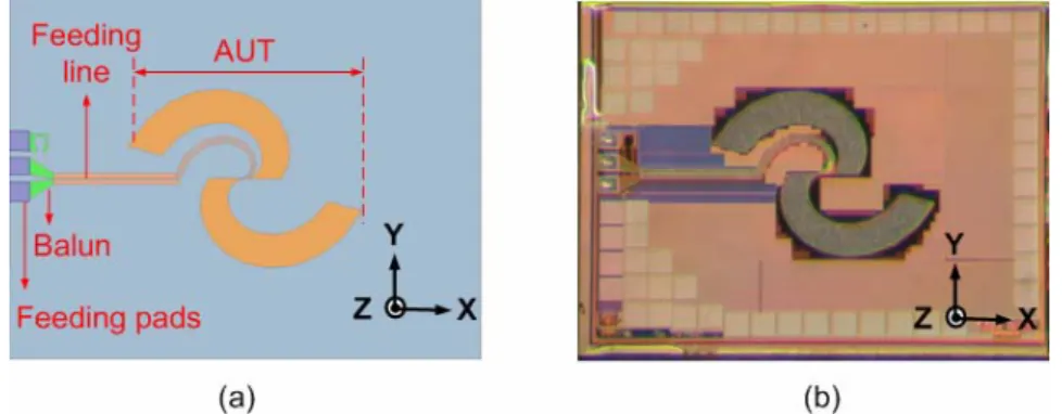
III Integrated spiral antenna on CMOS SOI technology...39
III.I CMOS SOI technology...39
III.II Integrated spiral antenna...41
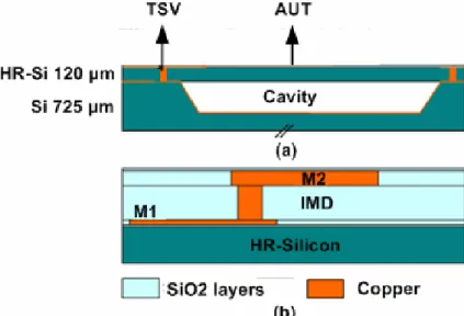
IV Integrated antenna on silicon interposer ...48
IV.I Fabrication process of CMOS interposer ...48
IV.II Integrated folded dipole ...49
V Dipole antenna ...53
VI Conclusion ...54
Chapter III...56
Characterization of probe-fed millimeter-wave integrated antennas ...56
I Introduction ...56
II Design of the characterization set-up ...56
Contents
II.I Hardware configuration ...56
II.II Instruments and program ...59
III RF probes ...61
III.I Introduction...61
III.II The structure of a standard RF on-wafer probe ...61
III.III The structure of two extended RF on-wafer probes ...63
IV. Example 1: Measurement of the integrated spiral antenna...67
V. Example 2: measurement of the integrated folded dipole antenna ...72
V.I Second test bench ...74
VI Conclusion ...78
Chapter IV...81
Characterization of integrated antennas at millimeter-wave frequencies with a flexible line...81
I Introduction ...81
II Choice of the substrate material ...82
III Design of the fixture ...84
IV Design of the transmission line...85
IV.I Main transmission line ...85
IV.II 2.40 mm-connector end design...88
IV.III GSG pads end...90
V Characterization of the flexible transmission line ...92
VI The connection between the t-line and the chip...97
VI.I Wire bonding ...97
VI.II Modified flip chip connection ...100
VII Characterization of the AUT...103
VII.I Comparison between simulation and experiment for the wirebonding technique105 VII.II Characterization with the AUT using the flip chip wirebonding ...107
VIII Conclusion...110
Chapter V ...113
Characterizing millimeter-wave antennas using Radar Cross-Section Measurement...113
I Introduction ...113
II Radar systems...113
III Application of the RCS method to antenna characterization...115
III.I Motivation...115
III.II Simulation model...116
IV Conclusion and future work...122
General conclusion and perspectives ...124
I Conclusion ...124
II Perspectives...125
List of abbreviations
List of abbreviations
The following table describes the significance of various abbreviations and acronyms used throughout the thesis.
Abbreviation Meaning
AC Alternating Current
ACP Air CoPlanar
Al Aluminum
APDs Avalanche Photo-Detectors
AR Axial ratio
Au Gold
AUT Antenna Under Test
BOX Buried OXide
CEPT European Conference of Postal and Telecommunications Administrations
CPS dB
CoPlanar Stripline Decibel
DC Direct Current
DUT Device Under Test
ECC Electronic Communications Committee EDFA
EFO
Erbium-doped fiber amplifier Electronic Flame-Off
FCC Federal Communications Commission GS Ground-Signal
GSG Ground-Signal-Ground HDMI
HR
High Definition Multimedia Interface High Resistivity
IC Integrated Circuits
IMD Inter Metal Dielectric
LTCC Low-Temperature Co-fired Ceramic MEMS
MMIC
MicroElectroMechanical Systems
Monolithic Microwave Integrated Circuits MZM Mach-Zehnder-Modulator PC polycarbonate
PD Photo-Detector PDMS
PEN
PolyDiMethylSiloxane PolyEthylene Naphthalate PES PolyEtherSulfone
PET Polyethylene terephthalate
PI PolyiMide
List of abbreviations
PMD Pre Metal dielectric
PR PhotoReceiver RCS Radio-Cross-Section Si3N4 Nitride
SiO2 Silicon oxide / Silicide SIP
SG
System In a Package Signal-Ground
SIW Substrate Integrated Waveguide
S-MMIC Submillimeter-wave Monolithic Integrated
SoC System On a Chip
SOI SOLT
Silicon On Insulator
Short-Open-Load-Through
STI Shallow Trench Isolation
TC Thermocompression
T-line Transmission line
TS TSV
Thermosonic
Through-Silicon-Vias US Ultrasonic
UTC-PD Uni-Ttravelling-Carrier Photo-Detector
VCO Voltage-Controlled Oscillator
VNA WLAN
Vector Network Analyzer Wireless Local Area Networks
WPAN Wireless Personal Area Networks
General Introduction
General Introduction
I Problem
There is increasing demand for high data-rate and short-range wireless communications. For instance, multi-Gbps high-definition media streams could be transmitted simultaneously between different devices in a household. The 60 GHz band is a good candidate for such applications as in the 60 GHz band a large free licensed spectrum is available. In this range of frequencies, there has recently been an intensive study of fully-integrated front-ends with low-directivity antennas using different micro-system technologies.
However due to the small size of millimeter-wave antennas (smaller or of the order of 1 mm in dimension) their characterization is sensitive to the testing environment. This is particularly the case for antennas with large beamwidth, eg omni-directional antennas, which are difficult to characterize as the size of the testing apparatus (such as RF probes, connecting bond wires and transmission lines) is much bigger than the AUT (antenna under test). One consequence is the masking effect caused by the apparatus on a significant angular sector of the radiation pattern. Another consequence is the reflection and scattering effects of the waves radiated by the antenna on the apparatus. Thus the characterization of integrated antennas has been a blocking point for the validation and further study of the integrated antennas at millimeter-wave frequencies.
II Objective of the thesis
In order to solve the problem, we firstly designed and fabricated an original 3D gain characterization test bench on which experiments were performed. This is a semi-automatic setup with a compact dimension of 90×60×65 cm3 and it is designed for integrated antennas with frequencies above 26 GHz.
Then we studied three techniques for feeding the AUT: the probe-fed technique, the flexible-transmission-line-fed technique and the RCS (Radio-Cross-Section) method.
First we address the probe-fed technique, where instead of using a standard probe
General Introduction
which provokes a limited effective scanning zoom [-10° 90°] and significant ripples, we propose two customized probes with a coaxial extension of 5 cm. One probe has a custom orientation for its connector and the other has a reversed orientation for its connector. Using these two customized probes, we significantly improve the performance of radiation gain pattern characterization: the scanning zone achieves [-50° 90°] for the long probe with customized connector and [-76° 90°] for the long probe with reversed connector. Furthermore, the ripples decrease with both customized probes.
Next we address the flexible-transmission-line-fed technique. The main advantage of this technique is that it is easy to use and the there is no masking zone. We used a flip-chip connection to avoid suspending bond wires thereby having better control of the impedance match. This technique improves the scanning zone to [-90° 90°].
Finally we study the radar-cross-section (RCS) method. In this technique, the AUT is connected to three different loads (50Ω, short, open). The simulation results demonstrate that there is insufficient variation in the ratio of received power to incident power as the load on the AUT is varied in order to make precise measurement with conventional measurement equipment.
This thesis was done in the laboratory IMEP-LAHC (l’Institut de Microélectronique Electromagnetisme et Photonique et LAboratoire d’Hyperfréquences et de Caractérisation) in cooperation with CEA-LETI (Commissariat à l'Energie Atomique - Laboratoire d'Electronique des Technologies de l'Information). The type of the thesis is a BDI (Bourses de docteur ingénieur), financed by the CNRS (Centre National de la Recherche Scientifique).
III Structure of the thesis
Chapter I presents the state of the art, pre-existing millimeter-wave test benches and some feeding techniques. These techniques include the probe-fed technique, waveguide-fed technique, transmission-line-fed technique, optical-link-fed technique and the VCO-fed technique.
Chapter II is a presentation of some antenna characteristics and two integrated antennas with low-directivity that we used for the radiation pattern characterization.
General Introduction
One is an integrated spiral antenna on CMOS SOI and the other one is an integrated folded dipole on high-resistivity silicon.
Chapter III presents a new 3D low-directivity integrated antenna test bench and a customized probe-fed technique.
Chapter IV presents the characterization of integrated antennas at millimeter-wave frequencies with a flexible line. To achieve this, we designed, fabricated and validated a transmission line on a flexible substrate. We connected this transmission line with the AUT using modified flip-chip technique.
Chapter V is about a feasibility study of characterization of an integrated antenna using a RCS method.
The thesis finishes with a general conclusion and outlook for future work.
Chapter I State of the art
Chapter I
State of the art
I Introduction
Millimeter waves are waves whose wavelength is between 1 mm to 10 mm. For electromagnetic waves in free space, this corresponds to frequencies roughly between 300 GHz and 30 GHz. The very first millimeter wave applications were in radio astronomy [1-4], and meteorology, where clouds and precipitation can be sensed with the help of a millimeter-wave radar, for instance to investigate the sizes, motions and distribution of cloud particles [5-9]. Millimeter waves are also widely used in military and defense applications [10-13]. More recently they are of substantial interest for commercial applications, such as short-range high date rate wireless communications in the 60 GHz band, such as automotive radar systems at the allocated frequency band of 76-77 GHz, which enable long-range intelligent cruise controls [14-17] and such as radar, imaging systems, remote sensing and active denial for the homeland security in the 94, 120 and 194 GHz bands [18-20].
There is a perceived latent demand for radio-communications at higher data-rates than the data-rates that are presently widely available for radio-communication. This has prompted the commercial sector, from startups to large multi-national companies, to investigate the appropriate choice of frequency bands for such applications.
Generally speaking, the outcome of these investigations is an investment in research and development in the 60 GHz band.
In particular there is a significant demand in the following high-data-volume markets:
short-range high-data-rate connections via Wireless Personal Area Networks (WPAN);
Wireless Local Area Networks (WLAN); and real-time video streaming wi-HDMI (high definition multimedia interface). The idea is that in future, multiple Gbps media streams will be shared simultaneously across multiple devices connected to the same WLAN.
The 60 GHz band is usually the selected candidate for such envisioned applications for three main reasons. Firstly, a large proportion of this band is free spectrum, as
Chapter I State of the art
shown in Table 1. In particular, no license is required in the US by the Federal Communications Commission (FCC) for this band, and in Europe, 9 GHz around the 60 GHz band is freely-licensed by the Electronic Communications Committee (ECC) of European Conference of Postal and Telecommunications Administrations (CEPT) [21]. One potential reason for requiring no license for this band is the high absorption and attenuation of such frequencies by oxygen and water (rain) which is illustrated by Figure 1.
This limitation is in fact the second reason for interest in the 60 GHz band for short-range applications. In other words, the high attenuation makes it possible to ensure some network security. Therefore, let us re-examine Figure 1. 1. Line A shows the attenuation as a function of frequency at sea level, at 20℃, a humidity density of 7.5 g m-3, while line B is for 4 km elevation, 0 ℃ and a humidity density of 1 g m-3 [18].
We can see that oxygen and water resonate at certain frequencies leading to a peak in attenuation in the 60 GHz band. Figure 1. 2 shows the atmospheric attenuation as a function of the rainfall rate. We can see that attenuation increases with frequency.
These attenuation characteristics limit the data transmission distance in the presence of oxygen and water, hence increasing network security. Finally, a third reason for interest in the 60 GHz band is its high propagation loss, since this loss leads to limited wall penetration, resulting in low likelihood of interference with other systems.
Table 1: Wireless unlicensed 60 GHz bands.
Region USA / Canada Europe Japan Korea Australia Band (GHz) 57.0-64.0 57.0-66.0 59.0-66.0 57.0-64.0 59.4-62.9
Figure 1. 1 Average atmospheric absorption of millimeter waves.
Chapter I State of the art
Figure 1. 2 Atmospheric attenuation due to rainfull rate.
The 60 GHz band can achieve a net data-rate of multiple gigabits per second over short distances [22]. Examples of applications are wireless gigabit Ethernet [23], and short-range wireless multimedia applications [24]. Furthermore in Japan, a wireless home link which can transmit broadcast TV signals from TV antennas to a TV set while also distributing them to other devices in the household has been presented in [25], while [24] proposes a scenario using dual-band operation (i.e. a 60 GHz system in combination with a 5 GHz WLAN) for the office and home environment.
The tendency in recent decades has been to make more cost-effective systems while preserving the same performance as older systems. Here, improving the cost-effectiveness corresponds to minimizing the substrate surface, and thus to integrating the entire millimeter meter wave system in a package (SiP) or even on a chip (SoC).
Some 60 GHz band highly-integrated transmitter- and receiver-chipsets for data transmission have been recently reported in [26-33,37-40]. They include front-end circuits such as power amplifiers (PA), low noise amplifiers (LNA), frequency multipliers, mixer, filters, voltage controlled oscillators (VCO), phase locked loops (PLL) and switchers. Integrated transceivers using CMOS technology have been described in [35-40].
A complete SoC should take fully-integrated antennas into consideraton as well as the transceiver. Early work in this direction has begun to appear, for instance [41]
Chapter I State of the art
presented a transistor amplifier integrated with a very simple 60 GHz microstrip array antenna with a simple etched pattern on an alumina substrate. References [34-36,42,43] present packaging of 60 GHz chip with an antenna. Reference [43]
gives a configuration of SIP with the antenna using LTCC technology. More recently, [44,45] presented low-directivity integrated antennas on CMOS SOI (Silicon On Insulator) substrates, while [46] presented an integrated folded dipole on high-resistivity silicon.
The size of such antennas is frequently smaller or of the order of 1 mm in dimension, and therefore is much smaller than modern probing devices. Thus, their radiation performance is difficult to characterize as they are perturbed by their testing environment such as RF probes, connecting bond wires and transmission lines. So in this chapter, firstly we present some existing test benches which were developed recently. Secondly we present some existing or preexisting techniques to characterize integrated antennas at millimeter wave frequencies. These techniques include the probe-fed technique, waveguide-fed technique, transmission-line-fed technique, optical-link-fed technique and the VCO-fed technique.
II Test benches
In the classical gain pattern characterization setup, the two antennas (i.e. the AUT and the measuring antenna which is usually a horn antenna) should be placed in the far-field range at same altitude above the ground. The horn antenna is fixed while the AUT rotates around its own positioner’s axis. The transmission energy is recorded by the apparatus at each position, and the Friis transmission equation is applied to get the radiation pattern in one plane. Subsequently, the AUT is rotated through 90° and the polarization of the horn antenna is changed to get all the co- and cross-polarization measurements of the E- and H- fields. Figure 1. 3 show the classical setup with the measuring antenna (horn antenna) on the left and the AUT on the right. The AUT is fixed on a motorized axis. This setup can be used up to several hundred GHz if the AUT is highly directive, but will not usually be suitable for other AUTs.
Chapter I State of the art
Figure 1. 3 Classical radiation pattern characterization setup.
At millimeter-wave frequencies and for millimeter-size antennas, the classical test bench is no-longer applicable. Instead, the radiation pattern is conventionally characterized with the help of a probe system. It is impractical to rotate the AUT with the probe system, thus the AUT is fixed and the measuring antenna rotates about two perpendicular horizontal axes with the AUT at the centre.
Several 3D radiation pattern measurement benches have been previously developed [47-57]. In [47,49,51,53], instead of being placed on a conventional probe station chuck, the AUT is placed on a extended thin dielectric sample holder. This minimizes the reflection and obstruction of the radiation pattern (Figure 1. 4 b). Rather than using a dielectric sample holder, [48] places an on-wafer AUT on top of a cavity filled with cavity resonance absorber (Figure 1. 5) which is suited for a cavity-backed superstrate antenna. Another way to minimize such reflection and obstruction is described in [47], which places the positioner and the probe leveling system outside an anechoic chamber,
Another important aspect of 3D radiation pattern measurement benches is the ability to measure at different angles, [49,51,53] describe a rotating arm where the measuring antenna is fixed. These rotating arms have two rotary stages and two rotary axes which enable different AUTs with different beam propagation senses.
References [49, 53] use two quarter-circle-shaped rotary stages (Figure 1. 4) while [51] uses two L-shaped rotary stages.
Normally, two polarizations (co- and cross- polarization) must be measured and the
Chapter I State of the art
conventional way to make these measurements is to rotate the measuring antenna manually or to insert a rotary waveguide. However [50] proposed that the horn antenna connects to a small motor by a belt. As the small motor is fixed on the rotating arm, this setup can achieve arbitrary polarizations.
Rather than having the measuring antenna rotate with the arm, [52,55,57] use a fixed curvilinear rail to guide the path of the measuring antenna. While [52] and [55] (Figure 1. 6 (a) and (b)) move the measuring antenna through a quarter-circle around the AUT, [57] is able to measure a half circle. Furthermore the setup described in [57] places the feeding probe in the upper hemi-sphere while measuring the radiation pattern in the lower hemi-sphere, thereby eliminating the influence of the feeding system (probe body) on the radiation pattern. On the other hand, the setup described in [57] is only applicable for AUTs with contacts on the backside of the antenna’s ground plane, since for AUTs with other contact configurations the RF probe would alter the radiation pattern.
Figure 1. 4 Photos of (a) the measurement setup in LEAT; (b) close up of the probe and AUT holders [49].
Chapter I State of the art
Figure 1. 5 Schematic of the setup for measurement of radiation pattern in the University of Michigan [48].
Figure 1. 6 (a) Schematic of the test bench with a quarter-circle above the AUT [52]; (b) Photo of a test bench with a quarter-circle of curvilinear rail above and to the side of the AUT [55].
Chapter I State of the art
Figure 1. 7 On-probe antenna measurement setup with backside probing technique. (a) Main parts of the proposed antenna measurement setup; (b) details on feeding from backside for aperture coupled antennas [57].
All the test benches presented above can be used for radiation pattern characterization with a standard-probe-fed technique, but they all have significant limitations. The curvilinear rails in [52,55] do not cover the whole range of measuring angles. All the techniques described in [47-56] fail to address the influence of the probe on the radiation pattern, and although the method in [57] manages to prevent this influence, this method is not applicable to most on-chip integrated antennas, which have the radiating element and the contact on the same metal layers. Finally, none of the above authors discuss the precision of the relative position of the probe and AUT although this is important because the radiation pattern can exhibit acute spatial variations.
In conclusion, it remains to design a test bench which covers the entire upper hemisphere, ensures precise relative positioning of the AUT and measuring antenna, is (semi-)automatic and minimizes the influence of the probe on the radiation pattern.
Perhaps this can be achieved by a non-standard probe feeding technique? Indeed we
Chapter I State of the art
discuss a suitable non-standard probe feeding technique in Chapter III.
III Probe-fed technique
The probe-fed technique is the conventional way to characterize radiation patterns for millimeter-wave frequencies. As reviewed in the previous section, all the test benches from references [47-57] used the probe-fed technique. One of the main problems with this technique is that millimeter-wave antennas are usually much smaller than modern probes (1 mm versus 2-3 cm), so that if we put a probe about 1 cm away from the AUT (as in [47-56]), there is a severe limitation on the angular sector over which measurements can be taken.
Furthermore the probe is typically metallic, which adds diffraction effects to the radiation pattern. To counteract this, a microwave absorbing material can be placed on the probe station’s metal surfaces. However, in view of the size of a probe, the absorber can induce even more masking effect on the radiation pattern – see Figure 1.
8. Reference [57] eliminates reflections / diffractions by placing the probe under the ground plane of the AUT, hence improving the angular sector available for measurement. However, this configuration is not applicable to most on-chip integrated antennas, which have the radiating element and the contact on the same metal layers (Figure 1. 7 b).
Figure 1. 8 Schematic of a test bench using probe-fed technique.
To improve on the previously proposed methods, we present two customized probes in Chapter III, that simultaneously maximize the angular range available for measurement while remaining compatible with most on-chip integrated antennas.
Chapter I State of the art
IV Transmission-line-fed technique
One way to improve the performance of previously-proposed measurement techniques [47-56] is to supply the AUT with a long feed line to extend the distance between the probe and the AUT. The feed line can be integrated on the same substrate as the AUT, as in [49, 51, 59], or it can be connected to the AUT via bond wires, as in [58]. One advantage of using bond wires is that multiple AUTs can be connected to the same measuring apparatus. However, bond wires are difficult to handle at such high frequencies, because it is difficult to maintain a good impedance matching and the wires may trigger parasitic radiation if they are too long. A V-connector is generally used as an interface between the feed line and the instrumentation [49, 58], but the transition between this connector and the feed line has to be carefully controlled to guarantee a good impedance matching, and the connector can also mask a part of the desired scanning zone.
Introducing a transmission line between a probe and the AUT or between a V-connector and the AUT reduces parasitic scattering from the probe or V-connector.
However, the masking effect remains unsolved, which is a major limitation when characterizing a low-directivity antenna.
(a) (b)
Figure 1. 9 (a) Slot antenna with feeding line and GSG pads in [51]; (b) planar antenna with feeding line and connector in [49].
To improve on the previously proposed methods, we use a transmission line made of a flexible substrate coupled with a flip-chip connection in Chapter IV, which simultaneously maximizes the range of available measurement angles and (attempts to) minimize parasitic radiation.
Chapter I State of the art
V Waveguide-fed technique
Another way to improve the standard probe-fed technique reviewed in Section II is to use a standard waveguide to feed the antenna. In [59-62], the authors describe feeding patch antennas with specially-designed waveguides located under the AUTs.
The electromagnetic energy couples to the AUT from the waveguide via a slot (Figure 1. 10). One disadvantage of this technique is that it is complicated to design a waveguide on the backside of an integrated AUT because a transition is needed between the feed line and the waveguide.
Some work on waveguide-to-microstrip transitions appears in [63-65]. Among these references [65] uses low-temperature co-fired (LTCC) technology at millimeter-wave frequencies. The final module consists of a 2×2antenna array, a microstrip line and a substrate integrated waveguide (SIW)-microstrip transition. It is mounted on and fed by a commercial waveguide flange WR 15 as shown in Figure 1. 13 (a) and (b).
While [65] proves the feasibility of a standard waveguide-fed technique, this technique is not very economical as it requires the complete design of a transition to feed the AUT from the rear (i.e. under the antenna) for every new AUT and every new technology (CMOS, LTCC, HTCC, GaAs, SiGe…).
Figure 1. 10 (a) Rectangular microstrip patch antenna; (b) cut-away view; from [61].
Chapter I State of the art
Figure 1. 11 General view of the waveguide to microstrip line transition [65].
Figure 1. 12 (a) Waveguide-to-microstrip transition layer stack; (b) top view of the 60 GHz patch antenna array including the waveguide transition [65].
Figure 1. 13 Photograph of the LTCC module (a) The top side of the antenna array is seen mounted on a waveguide flange; (b) the bottom side with the waveguide contacting metal ring around the air cavity [65].
Chapter I State of the art
VI Optically-fed technique
Another way to improve the standard probe-fed technique reviewed in Section II is an optically-fed technique. There are two main advantages of using an optical link rather than a coaxial cable to feed the AUT. First, it is possible to minimize masking effects as the feeding source can be placed far from the AUT. The transmission loss in optical fiber is negligible compared to a coaxial cable, so with the help of a long optical fiber, all the apparatus can be easily placed several meters away from the AUT (outside of the anechoic chamber) without any substantial loss. Second, optical fiber is not metallic thus it does not cause the any parasitic diffraction and reflection.
Some fibre-optical millimeter-wave transmission links use two horn antennas as their transmitting and measuring antennas. Thus a conventional photo-detector (PD) is used in [66-68]. However for integrated antennas, the big difference in scale between the PD and the AUT make it currently impractical to use a conventional PD for measurement. Rather, configurations involving the integration of a PD with an AUT are preferred [69-73].
Several recent works have investigated optically-fed structure with the use of different PD, such as pin PDs, uni-travelling-carrier photo-detector (UTC-PDs) and avalanche photo-detectors (APDs). This work investigated: planar antennas fed by a pin PD at 20 GHz [69] and at 25 GHz [70]; References [71-73, 76] are all fed by a UTC-PD and the AUTs in these works are: a 60 GHz slot antenna in [76]; a 120 GHz integrated slot antenna [71, 72]; and a 280 GHz integrated TEM horn [73]. Only in [70], the optical fibre is integrated with the AUT’s substrate and arrives in the active area of the PD.
The PDs described in [71-73,76] do not integrate the optical fibre, thus during the characterization of the AUT, a lensed fibre (i.e. with lenses between the end of the fibre and the PD) is used to point carefully to the active area of the PD (Figure 1. 17).
Figure 1. 14 presents a 20 GHz planar photonic band-gap dipole antenna fed by an integrated photo-detector (PIN photodiode) through a MMIC amplifier [69]. The dipole slot antenna is etched on a RT Duroid substrate.and the photo-detector is grown on a semi-insulating GaAs substrate. Figure 1. 15 shows the feeding chain of the measurement setup. A Mach-Zehnder-Modulator (MZM) modulates the optical carrier with an RF signal (fm=20 GHz) and the modulated signal is amplified by an Erbium-doped fiber amplifier (EDFA) and then divided by a power divider (D). The divided signal is coupled with the photo-detector which feeds the slot antenna.
Chapter I State of the art
Figure 1. 14 PBG antenna (ANT) with integrated photoreceiver (PR) and MMIC amplifier (A) [69].
Figure 1. 15 Measurement setup [69].
Figure 1. 16 shows a 120 GHz integrated photonic transmitter [72]. It consists of a CPW-fed slot antenna, a uni-traveling-carrier photodiode (UTC-PD) [74,75] and a Si lens. The slot antenna is fabricated on a high-resistivity Si substrate and the UTC-PD is flip-chip-bonded to the CPW pads. The photo-detector receives a 120 GHz sinusoidal optical wave (1.55 μm), then it generates a millimeter-meter wave which is transmitted to the slot antenna. Given the presence of the Si lens, the electric fields mainly radiate on the substrate side. The radiation power of the AUT is measured by a horn antenna through two Teflon lenses. The experimental setup for radiation power measurement shown in Figure 1. 17. The output power of the transmitter exceeds 100μw at 120 GHz.
Chapter I State of the art
Figure 1. 16 Diagram of the 120-GHz integrated photonic transmitter [72].
Figure 1. 17 Measurement setup of the transmitter [72].
Reference [76] demonstrates the feasibility of the integration of a photo-detector with an AUT at 60 GHz. However all the above references which operate at a frequency superior to 25 GHz have used lenses between the fibre and the PD. There are two consequences of this design: a risk of parasitic radiation originating from the support of these lenses; and a potential difficulty in ensuring the same coupling between the optical signal and the PD each time that the apparatus is set up. It is surprising that no-one has attempted to implement a lens-free characterization technique (i.e. with an optical fibre directly integrated with a photo-detector without lenses) for higher frequencies.
In conclusion, the integration of optical fibres with PDs will be necessary for successful implementation of the optically-fed technique for most AUTs (e.g. other than very simple cases such as slot antennas described in [76]) at 60 GHz or above.
VII VCO-fed technique
Integrated antennas may also be fed using a voltage-controlled oscillator (VCO)
Chapter I State of the art
[78-87]. References [78-80] present antennas integrated with a VCO for the X-band (8-12GHz), [81-83] for the K-band (18-26 GHz), [77,84-86] for the V-band (50-75GHz) and [87,88] for the sub-millimeter-wave band (300 GHz-1THz).
For RF signals, there are three ways to combine a VCO with an integrated antenna:
one is to have the VCO and the antenna integrated on the same substrate, e.g. at 21 GHz in [81] (Figure 1. 18 (a)) and at 60 GHz in [77] (Figure 1. 20); a second way is to use a flip-chip connection, although such flip-chip connections involve the use of an upside-down VCO; and a third way is to use bond wires e.g. [84] at 60 GHz (Figure 1.
19), but we do not believe that bond wires are a good solution at millimeter-wave frequencies.
These three methods may also be used to supply a VCO which is feeding an integrated antenna, bearing in mind that a VCO is a tunable circuit whose output frequency varies as a function of the input voltage and that a VCO itself needs to connect to a supply voltage. So firstly, we might use a standard probe system [89], but as described previously, this would cause masking effects, so it is not a good solution (Figure 1. 18 (b)). Secondly we might use bond wires and try to keep enough space between the AUT and the bond wires to avoid parasitic coupling and diffraction (Figure 1. 18 (a)). Finally, one might also use a flip chip connection.
The main advantage of using a VCO to feed an integrated antenna, relative to using a standard probe or a transmission line, as described in the previous sections, is that a VCO can be small compared to a standard probe or compared to the connector to a transmission line, and thus using a VCO can minimize reflections and parasitic radiation.
In conclusion, references [81, 77] prove the feasibility of the VCO-fed technique at 21 and 60 GHz. However this technique (similarly to the waveguide-fed technique) is not particularly economical as it is necessary to design an integrated VCO antenna circuit for each AUT. A VCO-fed technique with a flip-chip connection appears promising, but has not been previously investigated, and may be of interest for future work.
Chapter I State of the art
(a) (b) Figure 1. 18 Photo of (a) the 21 GHz chip (dipole antenna and VCO) under measurement [81] (1.5
×2.4 mm2) (b) the 60 GHz QVCO chip under measurement (0.7×0.65 mm2) [89].
Figure 1. 19 Photos of (a) a receiver chip (2.67×0.75 mm2) (b) 60 GHz LTCC SiP module [84].
Chapter I State of the art
Figure 1. 20 Photo of the 60 GHz impulse transmitter with integrated antenna [77].
VIII Conclusion
In this chapter, we presented several existing test benches and several feeding techniques for millimeter-wave frequencies, including the probe-fed technique, transmission-line-fed technique, waveguide-fed technique, optical-link-fed technique and the VCO-fed technique.
The angular-range limitation and parasitic reflection from the apparatus (a standard probe, a V-connector and wirebonding at 60 GHz band) are the two main problems with the standard-probe-fed and transmission-line-fed technique.
The standard-waveguide-fed, optically-fed and the VCO-fed techniques all concern the integration of the feeding source with the AUT. They could be implemented with the same or different technology as the AUT, but it may be challenging to ensure a good impedance match, for instance, using wire bonding in the 60 GHz band is not a good solution. It is possible to use several layers of LTCC to form a transition from a substrate-integrated waveguide to a microstrip line [65], however no-one has investigated this approach with other integrated technologies. VCOs are quite mature components for multiple technologies, they have been successfully integrated with antennas using the same technology, although this can be expensive, and it may be
Chapter I State of the art
interesting to attempt to connect a VCO to an AUT with a flip-chip connection. Finally, the optically-fed technique is quite promising however if the optical fibre is not integrated, but rather supplies a photodetector via lenses, it becomes necessary to build a positioning system which may also cause masking effects and parasitic reflection.
Thus, this thesis (as described in the overview of General Introduction) focuses on the standard-probe-fed and transmission-line-fed techniques and discusses improvements of these two techniques in Chapters III and IV, since these techniques are easy to reproduce and are suitable for most integrated on-chip antennas.
References:
[1] R. Wielebinski, “Microwaves -- The New Horizons of Radio Astronomy,” Microwave Conference, 1987. 17th European, pp. 19-24.
[2] J.W.M. Baars and H.J. Karcher, “Design features of the Large Millimeter Telescope (LMT),”
Antennas and Propagation Society International Symposium, 1999. IEEE, pp. 1544-1547 vol.1543.
[3] J. Davis and J. Cogdell, “Astronomical refraction at millimeter wavelengths,” Antennas and Propagation, IEEE Transactions, vol. 18, no. 4, 1970, pp. 490-493.
[4] A.Karpov, “Optimizing receivers for ground based mm-wave radio telescopes,” proceeding of the 2th ESA workshop on millimeter wave thchnology and applications. IRAM technical report 250/98, 1998.
[5] J.B. Mead, A.L. Pazmany, S.M. Sekelsky and R.E. McIntosh, “Millimeter-wave radars for remotely sensing clouds and precipitation,” Proceedings of the IEEE, vol. 82, no. 12, 1994, pp. 1891-1906.
[6] R.P. Bambha, J.R. Carswell, J.B. Mead and R.E. McIntosh, “A compact millimeter wave radar for airborne studies of clouds and precipitation,” Geoscience and Remote Sensing Symposium Proceedings, 1998. IGARSS '98. 1998 IEEE International, pp. 443-445 vol.441.
[7] J.R. Wang and P. Racette, “Airborne millimeter-wave radiometric observations of cirrus clouds,”
Geoscience and Remote Sensing, 1997. IGARSS '97. Remote Sensing - A Scientific Vision for Sustainable Development., 1997 IEEE International, pp. 1737-1739 vol.1734.
[8] T. Toshiaki, Y. Jun, A. Hideji, F. Ken-ichi, Y. Shin-ichi, K. Hiroshi, A. Ken-ichi, K. Youhei, O.
Yuichi, T. Tamio, N. Teruyuki, O. Hajime, F. Yasushi and S. Nobuo, “Observations of cloud properties using the millimeter- wave FM-CW radar of Chiba Univ,” Microwave Conference, 2006. APMC 2006.
Asia-Pacific, pp. 560-563.
[9] T. Takano, Y. Nakanishi, H. Abe, J. Yamaguchi, S.I. Yokote, K.I. Futaba, Y. Kawamura, H. Kumagai, Y. Ohno, T. Takamura and T. Nakajima, “Performance of a Developed Low-Power and High-Sensitivity Cloud Profiling Millimeter-wave Radar : FALCON-I,” Microwave Conference, 2007.
APMC 2007. Asia-Pacific, pp. 1-4.
[10] J.H. Wehling, “Multifunction millimeter-wave systems for armored vehicle application,”
Microwave Theory and Techniques, IEEE Transactions, vol. 53, no. 3, 2005, pp. 1021-1025.
[11] D.N. McQuiddy, Jr., “High volume applications for GaAs microwave and millimeter-wave ICs in
Chapter I State of the art
military systems,” Gallium Arsenide Integrated Circuit (GaAs IC) Symposium, 1989. Technical Digest 1989., 11th Annual, pp. 3-6.
[12] V.I. Antyufeev, V.N. Bykov, A.M. Grichaniuk, V.A. Krayucshkin and S.A. Shilo, “Radiometric observability estimation of military equipment samples in a millimeter-wave band,” Physics and Engineering of Microwaves, Millimeter, and Submillimeter Waves, 2004. MSMW 04. The Fifth International Kharkov Symposium on, pp. 196-198 Vol.191.
[13] J. Altmannm, “Millimetre Waves, Lasers, Acoustics for Non-Lethal Weapons? Physics Analyses and Inferences,” Technical University of Dortmund, 2008.
[14] M. Schneider, "Automotive Radar – Status and Trends," Proc.German Microwave Conference GeMiC, Ulm, Germany, pp. 144-147.
[15] I. Gresham, N. Jain, T. Budka, A. Alexanian, N. Kinayman, B. Ziegner, S. Brown and P. Staecker,
“A compact manufacturable 76-77-GHz radar module for commercial ACC applications,” Microwave Theory and Techniques, IEEE Transactions, vol. 49, no. 1, 2001, pp. 44-58.
[16] D.M. Grimes, and T.O. Jones, “Automotive radar: A brief review,” Proceedings of the IEEE, vol.
62, no. 6, 1974, pp. 804-822.
[17] Australian communications Authority, “A review of automotive radar systems - devices and regulatory frameworks,” 2001.
[18] K-C. Huang and Z. Wang, “Millimeter Wave Communication Systems,” John Wiley & Sons, 2011.
[19] I. Chee-Hong Lai amd M. Fujishima, “Design and Modeling of Millimeter-Wave CMOS Circuits for Wireless Transceivers,” Springer, 2008.
[20] D.X. Liu, U. Pfeiffer and J. Grzyb, “Advanced Millimeter-Wave Technologies: Antennas, Packaging and Circuits”, John Wiley & Sons, 2009.
[21] D. Wang and N. Cahoon, “60 GHz high speed wireless link - technology and design challenges,”
Solid-State and Integrated-Circuit Technology, 2008. ICSICT 2008. 9th International Conference. pp.
1343-1347.
[22] P. Smulders, Y. Haibing and I. Akkermans, “On the Design of Low-Cost 60-GHz Radios for Multigigabit-per-Second Transmission over Short Distances [Topics in Radio Communications],”
Communications Magazine, IEEE, 45 (2007), 44-51.
[23] K. Ohata, K. Maruhashi, M. Ito, S. Kishimoto, K. Ikuina, T. Hashiguchi, K. Ikeda and N.
Takahashi, “1.25 Gbps wireless Gigabit ethernet link at 60 GHz-band,” Radio Frequency Integrated Circuits (RFIC) Symposium, 2003 IEEE, Philadelphia, 2003.
[24] P. Smulders, “Exploiting the 60 GHz band for local wireless multimedia access: prospects and future directions,” Communications Magazine, IEEE, 40 (2002), 140-147.
[25] K. Hamaguchi, Y. Shoji, H. Ogawa, H. Sato, K. Tokuda, Y. Hirachi, T. Iwasaki, A. Akeyama, K.
Ueki and T. Kizawa, “A wireless video home-link using 60 GHz band: Concept and performance of the developed system,” Proc. 30th Eur. Microw. Conf., Paris, France, Oct. 2–6, 2000, vol. 1, pp. 293–296.
[26] M. Siddiqui, M. Quijije, A. Lawrence, B. Pitman, R. Katz, P. Tran, A. Chau, D. Davison, S. Din, R.
Lai and D. Streit, “GaAs components for 60 GHz wireless communication applications,” GaAs Mantech Conf. Tech. Dig., San Diego, CA, Apr. 11, 2002, pp. 243–246.
[27] K. Fujii, M. Adamski, P. Bianco, D. Gunyan, J. Hall, R. Kishimura, C. Lesko, M. Schefer, S.
Hessel, H. Morkner and A. Niedzwiecki, “A 60 GHz MMIC chipset for 1-Gbit/s wireless links,” IEEE MTT-S Int. Microw. Symp. Dig., Seattle, WA, Jun. 2–7, 2002, vol. 3, pp. 1725–1728.
[28] O. Vaudescal, B. Lefebvre, V. Lehoué and P. Quentin, “A highly integrated MMIC chipset for 60
Chapter I State of the art
GHz broadband wireless applications,” IEEE MTT-S Int. Microw. Symp. Dig., Seattle, WA, Jun. 2–7, 2002, vol. 3, pp. 1729–1732.
[29] Y. Mimino, K. Nakamura, Y. Hasegawa, Y. Aoki, S. Kuroda and T. Tokumitsu, “A 60 GHz millimeter-wave MMIC chipset for broadband wireless access system front-end,” IEEE MTT-S Int.
Microw. Symp. Dig., Seattle, WA, Jun. 2–7, 2002, vol. 3, pp. 1721–1724.
[30] H. Zirath, T. Masuda, R. Kozhuharov and M. Ferndahl, “Development of 60 GHz front-end circuits for a high-data-rate communication system,” IEEE J. Solid-State Circuits, vol. 39, no. 10, pp.
1640–1649, Oct. 2004.
[31] B. A. Floyd, S. K. Reynolds, U. R. Pfeiffer, T. Zwick, T. Beukema, and B. Gaucher, “SiGe bipolar transceiver circuits operating at 60 GHz,” IEEE J. Solid-State Circuits, vol. 40, no. 1, pp. 156–167, Jan.
2005.
[32] S. E. Gunnarsson, C. Kärnfelt, H. Zirath, R. Kozhuharov, D. Kuylenstierna, A. Alping and C.
Fager, “Highly integrated 60 GHz transmitter and receiver MMICs in a GaAs pHEMT technology,”
IEEE J. Solid-State Circuits, vol. 40, no. 11, pp. 2174–2186, Nov. 2005.
[33] J. Mizoe, S. Amano, T. Kuwabara, T. Kaneko, K. Wada, A. Kato, K. Sato and M. Fujise, “Minature 60 GHz transmitter/receiver modules on AlN multi-layer high temperature co-fired ceramic,” IEEE MTT-S Int. Microw. Symp. Dig., Anaheim, CA, Jun. 13–19, 1999, vol. 2, pp. 475–478.
[34] J.M. Gilbert, C.H. Doan, S. Emami and C.B. Shung, “A 4-Gbps Uncompressed Wireless HD A/V Transceiver Chipset,” Micro, IEEE, vol. 28, no. 2, 2008, pp. 56-64.
[35] S.K. Reynolds, B.A. Floyd, U.R. Pfeiffer, T. Beukema, J. Grzyb, C. Haymes, B. Gaucher and M.
Soyuer, “A Silicon 60-GHz Receiver and Transmitter Chipset for Broadband Communications,”
Solid-State Circuits, IEEE Journal, vol. 41, no. 12, 2006, pp. 2820-2831.
[36] S. Pinel, S. Sarkar, P. Sen, B. Perumana, D. Yeh, D. Dawn and J. Laskar, “A 90nm CMOS 60GHz Radio,” Solid-State Circuits Conference, 2008. ISSCC 2008. Digest of Technical Papers. IEEE International, pp. 130-601.
[37] C. H. Doan, S. Emami, D. A. Sobel, A. M. Niknejad and R. W. Brodersen, “Design considerations for 60 GHz CMOS radios,” IEEE Commun. Mag., pp. 132–140, Dec. 2004.
[38] B. Razavi, “A 60-GHz CMOS receiver front-end,” Solid-State Circuits, IEEE Journal, vol. 41, no.
1, 2006, pp. 17-22.
[39] C. Marcu, D. Chowdhury, C. Thakkar, K. Ling-Kai, M. Tabesh, P. Jung-Dong, W. Yanjie, B.
Afshar, A. Gupta, A. Arbabian, S. Gambini, R. Zamani, A.M. Niknejad and E. Alon, “A 90nm CMOS low-power 60GHz transceiver with integrated baseband circuitry,” Solid-State Circuits Conference - Digest of Technical Papers, 2009. ISSCC 2009. IEEE International, pp. 314-315.
[40] M. Tanomura, Y. Hamada, S. Kishimoto, M. Ito, N. Orihashi, K. Maruhashi and H. Shimawaki,
“TX and RX Front-Ends for 60GHz Band in 90nm Standard Bulk CMOS,” Solid-State Circuits Conference, 2008. ISSCC 2008. Digest of Technical Papers. IEEE International, pp. 558-635.
[41] C. Karnfelt, P. Hallbjorner, H. Zirath and A. Alping, “High gain active microstrip antenna for 60-GHz WLAN/WPAN applications,” Microwave Theory and Techniques, IEEE Transactions, vol. 54, no. 6, 2006, pp. 2593-2603.
[42] Y.P. Zhang and D. Liu, “Antenna-on-chip and antenna-in-package solutions to highly integrated millimeter-wave devices for wireless communications,” Antennas and Propagation, IEEE Transactions, vol. 57, no. 10, 2009, pp. 2830-2841.
[43] T. Seki, K. Nishikawa, I. Toyoda, and S. Kubota, “Microstrip Array Antenna with Parasitic Elements Alternately Arranged Over Two Layers of LTCC Substrate for Millimeter Wave
Chapter I State of the art
Applications,” Radio and Wireless Symposium, 2007 IEEE, pp. 149-152.
[44] M. Barakat, C. Delaveaud and F. Ndagijimana, “Performance of a 0.13μm SOI integrated 60 GHz dipole antenna,” IEEE Antennas and Propagation Society International Symposium, Honolulu, HI, 2007.
[45] M. Barakat, C. Delaveaud, F. Ndagijimana, “Circularly Polarized Antenna on SOI for the 60 GHz Band,” Antennas and Propagation, EuCAP 2007, Edinburgh, 2007.
[46] L. Dussopt et al., “Silicon Interposer with Integrated Antenna Array for Millimeter-Wave Short-Range Communications,” submitted to IEEE MTT-S Int. Microwave Symp., 17-22 jun.
2012, Montreal, Canada.
[47] T. Zwick, C. Baks, U. Pfeiffer, D. Liu, and B. Gaucher, “Probe based MMW antenna measurement setup,” IEEE Antennas and Propagation Society International Symposium, Montery CA, 2004.
[48] K. Van Caekenberghe, K. Brakora, W. Hong, K. Jumani, D. Liao, M. Rangwala, Y. Wee, X. Zhu and K. Sarabandi, “A 2–40 GHz Probe Station Based Setup for On-Wafer Antenna Measurements,”
Antennas and Propagation, IEEE Transactions, 56 (2008), 3241-3247.
[49] S. Ranvier, M. Kyrö, C. Icheln, C. Luxey, R. Staraj and P. Vainikainen, “Compact 3-D on-wafer radiation pattern measurement system for 60 GHz antennas,” Microwave and Optical Technology Letters, 51 (2009), 319-324.
[50] R. Simons, N.G.R. Center “Novel on-wafer radiation pattern measurement technique for MEMS actuator based reconfigurable patch antennas,” National Aeronautics and Space Administration, Glenn Research Center, 2003.
[51] S. Beer, G.. Adamiuk and T. Zwick, “Design and probe based measurement of 77 GHz antennas for antenna in package applications,” Microwave Conference, EuMC 2009, Rome, 2009.
[52] N. Segura, S. Montusclat, C. Person, S. Tedjini and D. Gloria, “On-wafer radiation pattern measurements of integrated antennas on standard BiCMOS and glass processes for 40-80GHz applications,” Microelectronic Test Structures, ICMTS 2005, Leuven, 2005.
[53] D. Titz, M. Kyro, F.B. Abdeljelil, C. Luxey, G. Jacquemod and P. Vainikainen, “Design and measurement of a dipole-antenna on a 130nm CMOS substrate for 60GHz communications,” ICECom 2010, Dubrovnik, 2010.
[54] P. Bo, L. Yuan, G.E. Ponchak, J. Papapolymerou and M.M. Tentzeris, “A 60-GHz CPW-Fed High-Gain and Broadband Integrated Horn Antenna,” Antennas and Propagation, IEEE Transactions, 57 (2009), 1050-1056.
[55] R. Pilard, S. Montusclat, D. Gloria, F. Le Pennec and C. Person, “Dedicated measurement setup for millimetre-wave silicon integrated antennas: BiCMOS and CMOS high resistivity SOI process characterization,” Antennas and Propagation, EuCAP 2009, Berlin, 2009.
[56] J. Lanteri, L. Dussopt, R. Pilard, D. Gloria, S.D. Yamamoto, A. Cathelin and H. Hezzeddine, “60 GHz antennas in HTCC and glass technology,” EuCAP2010, Barcelona, 2010.
[57] K. Mohammadpour-Aghdam, S. Brebels, A. Enayati, R. Faraji-Dana, G.A.E. Vandenbosch and W.
DeRaedt, “RF probe influence study in millimeter-wave antenna pattern measurements,” International Journal of RF and Microwave Computer-Aided Engineering, 21 (2011).
[58] M. Barakat, “Dispositif radiofrequence millimetrique pour objets communicants de type smart dust,” Ph.D thesis, Grenoble university, Grenoble, 2008.
[59] E. Marzolf and M.h.Drissi, “Waveguide-fed planar antennas for millimeter waveband,”
Microwave and Optical Technology Letters, 35, (2002), 71-73.
[60] J. Hirokawa, M. Ando and N. Goto, “Waveguide-fed parallel plate slot array antenna,” Antennas
Chapter I State of the art
and Propagation, IEEE Transactions, 40 (1992), 218-223.
[61] M. Kanda, D.C. Chang and D.H. Greenlee, “The Characteristics of Iris-Fed Millimeter-Wave Rectangular Microstrip Patch Antennas,” Electromagnetic Compatibility, IEEE Transactions, vol.
EMC-27, no. 4, 1985, pp. 212-220.
[62] K. Sudo, A. Akiyama, J. Hirokawa and M. Ando, “A millimeter-wave radial line slot antenna fed by a rectangular waveguide through a ring slot,” Antennas and Propagation Society International Symposium, 2001. IEEE, pp. 254-257 vol.252.
[63] A. Artemenko, A. Maltsev, R. Maslennikov, A. Sevastyanov and V. Ssorin, “Design of wideband waveguide to microstrip transition for 60 GHz frequency band,” Microwave Conference (EuMC), 2011 41st European, pp. 838-841.
[64] T.H. Yang, C.F. Chen, T.Y. Huang, C.L. Wang and R.B. Wu, “A 60GHz LTCC transition between microstrip line and substrate integrated waveguide,” APMC 2005, Suchou, 2005.
[65] F. Wollenschlager, L. Alhouri, L. Xia, S. Rentsch, J. Muller, R. Stephan, and M.A. Hein,
“Measurement of a 60 GHz antenna array fed by a planar waveguide-to-microstrip transition integrated in low-temperature co-fired ceramics,” Antennas and Propagation, 2009. EuCAP 2009. 3rd European Conference, pp. 1001-1005.
[66] N. Imai, S. Banba, E. Suematsu and H. Sawada, “Millimeter-wave fiber optic technologies for subcarrier transmission systems,” Microwave Conference, 1994. 24th European, pp. 1465-1470.
[67] T. Shao, F. Paresys, Y. Le Guennec, G. Maury, N. Corrao and B. Cabon, “Photonic generation and radio transmission of ECMA 387 signal at 60 GHz using WDM demultiplexer,” Microwave and Optical Technology Letters, vol. 54, no. 2, 2012, pp. 275-277.
[68] D. Wake, N.G. Walker and I.C. Smith, “A fibre-fed millimetre-wave radio transmitter with zero electrical power requirement,” Microwave Conference, 1993. 23rd European, pp. 116-118.
[69] G.A. Chakam and W. Freude, “Coplanar phased array antenna with optical feeder and photonic bandgap structure,” Microwave Photonics, 1999. MWP '99. International Topical Meeting, pp. 1-4 suppl.
[70] M. Khodier and C. Christodoulou, “Optically driven CPW-fed slot antenna for wireless communications,” Antennas and Propagation for Wireless Communications, 2000 IEEE-APS Conference, pp. 121-124.
[71] N. Sahri and T. Nagatsuma, “Packaged photonic probes for an on-wafer broad-band millimeter-wave network analyzer,” Photonics Technology Letters, IEEE, vol. 12, no. 9, 2000, pp.
1225-1227.
[72] A. Hirata, N. Sahri, H. Ishii, K. Machida, S. Yagi and T. Nagatsuma, “Design and characterization of millimeter-wave antenna for integrated photonic transmitter,” Microwave Conference, 2000 Asia-Pacific, pp. 70-73.
[73] G. Ducournau, A. Beck, D. Ducatteau, E. Peytavit, T. Akalin and J. Lampin, “Radiation pattern measurements of an integrated TEM horn antenna,” Infrared Millimeter and Terahertz Waves (IRMMW-THz), 2010 35th International Conference, pp. 1-2.
[74] T. Ishibashi et al., “High Power Uni-Traveling-Carrier Photodiodes,” MWP’99, pp 75-78, 1999.
[75] T. Nagatsuma et al., “All Optoelectronic Generation and Detection of Millimeter-Wave Signals,”
MWP’98, pp 5-8, 1998.
[76] K. Li, J.X. Ge, T. Matsui and M. Izutsu, “High output photodetector and CPW-fed slot antenna array for millimeter-wave fiber-radio system,” Computational Electromagnetics and Its Applications, 1999. Proceedings. (ICCEA '99) 1999 International Conference, pp. 337-340.
Chapter I State of the art
[77] A. Siligaris, N. Deparis, R. Pilard, D. Gloria, C. Loyez, N. Rolland, L. Dussopt, J. Lantéri, R. Beck, P. Vincent, "A 60 GHz UWB impulse radio transmitter with integrated antenna in CMOS 65 nm SOI technology," 11th IEEE Topical Meeting on Silicon Monolithic Integrated Circuits in RF Systems, Phoenix, 17-19 January 2011.
[78] C.C. Hu, C.F. Jou, and J.J. Wu, “Two-dimensional beam-scanning linear active leaky-wave antenna array using coupled VCOs,” Microwaves, Antennas and Propagation, IEE Proceedings, vol.
147, no. 1, 2000, pp. 68-72.
[79] K. Nien-An, H. Cheng-Chi, W. Jin-Jei and C.F. Jou, “Active aperture-coupled leaky-wave antenna,” Electronics Letters, vol. 34, no. 23, 1998, pp. 2183-2184.
[80] F. Touati and M. Pons, “On-chip integration of dipole antenna and VCO using standard BiCMOS technology for 10 GHz applications,” Solid-State Circuits Conference, 2003. ESSCIRC '03.
Proceedings of the 29th European, pp. 493-496.
[81] M. Pons, F. Touati, and P. Senn, “Study of on-chip integrated antennas using standard silicon technology for short distance communications,” Wireless Technology, 2005. The European Conference, pp. 253-256.
[82] C. Changhua, D. Yanping, Y. Xiuge, L. Jau-Jr, W. Hsin-Ta, A.K. Verma, L. Jenshan, F. Martin, and K.K. O, “A 24-GHz Transmitter With On-Chip Dipole Antenna in 0.13μm CMOS,” Solid-State Circuits, IEEE Journal of, vol. 43, no. 6, 2008, pp. 1394-1402.
[83] P.K. Talukder, M. Neuner, C. Meliani, F.J. Schmuckle and W. Heinrich, “A 24 GHz Active Antenna in Flip-Chip Technology with Integrated Frontend,” Microwave Symposium Digest, 2006.
IEEE MTT-S International, pp. 1776-1779.
[84] L. Jae Jin, J. Dong Yun, E. Ki Chan, O. Inn Yeal, and P. Chul Soon, “A low power CMOS single-chip receiver and system-on-package for 60GHz mobile applications,” Radio-Frequency Integration Technology, 2009. RFIT 2009. IEEE International Symposium on, pp. 24-27.
[85] G. Passiopoulos, S. Nam, A. Georgiou, A. Baree, I.D. Robertson and E.A. Grindrod, “V-Band MMIC Chip-Set, Design and Performance,” Microwave Conference, 1998. 28th European, pp.
157-162.
[86] H.K. Chiou, I.S. Chen and W.C. Chen, “High gain V-band active-integrated antenna transmitter using Darlington pair VCO in 0.13μm CMOS process,” Electronics Letters, vol. 46, no. 5, 2010, pp.
321-322.
[87] K.O. Kenneth, “Sub-millimeter wave CMOS integrated circuits and systems,” Radio-Frequency Integration Technology (RFIT), 2011 IEEE International Symposium on, pp. 1-8.
[88] S. Eunyoung, C. Changhua, S. Dongha, D.J. Arenas, D.B. Tanner, H. Chin-Ming, and K.K. O, “A 410GHz CMOS Push-Push Oscillator with an On-Chip Patch Antenna,” Solid-State Circuits Conference, 2008. ISSCC 2008. Digest of Technical Papers. IEEE International, pp. 472-629.
[89] A. Barghouthi, A. Krause, C. Carta, F. Ellinger, and C. Scheytt, “Design and Characterization of a V-Band Quadrature VCO Based on a Common-Collector SiGe Colpitts VCO,” Compound Semiconductor Integrated Circuit Symposium (CSICS), 2010 IEEE, pp. 1-3.
Chapter II Antenna under test (AUT)
Chapter II
Antenna under test (AUT)
I Introduction
In this chapter, we are going to present some antenna characteristics and three millimeter-wave antennas under test we used for the radiation pattern characterization:
an integrated spiral antenna on CMOS SOI and an integrated folded dipole on high-resistivity silicon.
II Antenna characteristics
Several antennas’ parameters definitions will be reminded in this section, these definitions will help to describe the performance of an antenna. These parameters are following items: the radiation gain, the polarization, the radiation pattern, the input impedance, the radiation efficiency, the bandwidth, the axial ratio, far field and near field regions and the Friis transmission equation [1,2].
II.I Radiation gain
Radiation gain is one of the factors describing an antenna performances. Absolute gain of an antenna in a given direction is defined as the ratio of the radiation intensity flowing in that direction to the radiation intensity that would be obtained if the power accepted by the antenna were radiated isotropically. If the direction is not specified, the direction of maximum radiation intensity is usually implied. Antenna gain is expressed in dBi.
PAcc
G= 4π⋅U(θ,ϕ) (3.1)
( )
20 2
2
, 1 E r
Uθ ϕ = η (3.2)
Where
( )
θ,ϕU is the radiation intensity in watts per steradian,
Chapter II Antenna under test (AUT)
|E| is the magnitude of the E-field,
η0 is the intrinsic impedance of free space, 377 ohms.
The total gain can be expressed in two orthogonal component θ and φ, θ is rotates away from the z-axis and φ is rotates away from the x-axis. The spherical coordinate system is shown in Figure 2. 1
ϕ
θ G
G
G= + (3.3)
The partial gains Gθ and Gφ are expressed as following:
Pin
Gθ =4πUθ (3.4)
Pin
Gϕ 4πUϕ
= (3.5)
Figure 2. 1 Spherical coordinate system for antenna characterisation.
II.II Polarization
Polarization of an antenna in a given direction is defined as “the polarization of the wave transmitted by the antenna” which means “that the property of an electromagnetic wave describing the time varying direction and relative magnitude of the electric-field vector, specially, the figure traced as a function of time by the extremity of the vector at a fixed location in space, and the sense in which it is traced, as observed along the direction of the propagation” [1]. The polarization can be classified into different categories.
Chapter II Antenna under test (AUT)
II.II.I Co-polarization and cross-polarization
At each point of the radiation sphere the polarization is usually resolved in two components: a co-polarization and a cross-polarization component. The co-polarization is a reference polarization, which can be linear or circular and usually corresponds to the desired antenna polarization. The cross-polarization is orthogonal to the co-polarization.
II.II.II Linear, circular and elliptical polarizations:
Here we suppose that the electromagnetic wave propagate along z direction and the three components Ex, Ey and Ez along XYZ directions of the electrical field Er
are given by equation 3.6.
⎟⎟
⎟
⎠
⎞
⎜⎜
⎜
⎝
⎛
+
− +
−
⎟=
⎟⎟
⎠
⎞
⎜⎜
⎜
⎝
⎛
=
0
) (
) (
0 0
Y Y
X X
Z Y X
kt wt Cos E
kt wt Cos E
E E E
E φ
r φ
(3.6)
Ex0, Ey0 and Ez0 are the maximum magnitude of the electrical field in their respective direction.
According to the different situation, the polarization can be classified into three forms as following:
Linear polarization
The electric field is linearly polarized when
,Δφ=φY −φX =nπ, n is an integer (3.7) The vector which describes the electric field at a point in space as a function of time is always directed along a line (Figure 2. 2 ).
Figure 2. 2 Linear polarization.
Chapter II Antenna under test (AUT)
The pyramidal horn antenna radiates a linear polarization, the E plane is shown in the Figure 2. 3:
Figure 2. 3 E-plane for a pyramidal horn antenna.
Circular polarization
The field is circularly polarized when equations 3.9 and 3.10 are satisfied (Figure 2.
4):
0 0 Y
X E
E = (3.8)
. 2 2
1π π
φ φ
φ = Y − X = + n
Δ , n is an integer. (3.9)
The electric field has two orthogonal linear components and these two components have the same magnitude and the time-phase difference of odd multiple of 90°.
Figure 2. 4 Circular polarization.
According to the sense of the rotation is viewed as the wave travels from the observer, the circular polarization can be defined as clockwise polarization and counterclockwise polarization. If the rotation is clockwise, the wave is right-hand circularly polarized, if the rotation is counterclockwise, the wave is left-handed circularly polarized.
Chapter II Antenna under test (AUT)
for clockwise
⎪⎪
⎩
⎪⎪⎨
⎧
⎟ =
⎠
⎜ ⎞
⎝⎛ + +
⎟ =
⎠
⎜ ⎞
⎝⎛ +
−
= Δ
...
3 , 2 , 1 , 0 , 2 2
1
...
3 , 2 , 1 , 0 , 2 2
1
n n
n n
π π φ
for counterclockwise
(3.10)
Elliptical polarization
Elliptical polarization is more general than linear or circular polarization. Linear and circular polarizations are special cases of elliptical polarization.
The field is elliptical polarized when
and/or
The elliptical polarization (Figure 2. 5) corresponds to the general case where the two field components are of different magnitude and/or not in phase quadrature
Figure 2. 5 Elliptical polarization.
II.III Radiation pattern
An antenna radiation pattern or antenna pattern is defined as "a mathematical function or graphical representation of the radiation properties of the antenna as a function of space coordinates. In most cases, the radiation pattern is determined in the far-field region and is represented as a function of the directional coordinates." [1].
the radiation property of most concern is the two- or three-dimensional spatial distribution of radiated energy as a function of an observer's position along a path or
0 0 Y
X E
E ≠ (3.11)
π φ
φ
φ 2
n
X
Y − ≠±
=
Δ , n is integer (3.12)
![Figure 1. 4 Photos of (a) the measurement setup in LEAT; (b) close up of the probe and AUT holders [49]](https://thumb-eu.123doks.com/thumbv2/1bibliocom/459781.66815/18.892.135.754.560.827/figure-photos-measurement-setup-leat-close-probe-holders.webp)
![Figure 1. 9 (a) Slot antenna with feeding line and GSG pads in [51]; (b) planar antenna with feeding line and connector in [49]](https://thumb-eu.123doks.com/thumbv2/1bibliocom/459781.66815/22.892.150.740.645.893/figure-slot-antenna-feeding-planar-antenna-feeding-connector.webp)
![Figure 1. 11 General view of the waveguide to microstrip line transition [65].](https://thumb-eu.123doks.com/thumbv2/1bibliocom/459781.66815/24.892.279.617.115.473/figure-general-view-waveguide-microstrip-line-transition.webp)
![Figure 1. 12 (a) Waveguide-to-microstrip transition layer stack; (b) top view of the 60 GHz patch antenna array including the waveguide transition [65]](https://thumb-eu.123doks.com/thumbv2/1bibliocom/459781.66815/24.892.159.733.535.705/figure-waveguide-microstrip-transition-antenna-including-waveguide-transition.webp)
![Figure 1. 19 Photos of (a) a receiver chip (2.67×0.75 mm 2 ) (b) 60 GHz LTCC SiP module [84]](https://thumb-eu.123doks.com/thumbv2/1bibliocom/459781.66815/29.892.147.746.120.362/figure-photos-receiver-chip-ghz-ltcc-sip-module.webp)
![Figure 1. 20 Photo of the 60 GHz impulse transmitter with integrated antenna [77].](https://thumb-eu.123doks.com/thumbv2/1bibliocom/459781.66815/30.892.266.627.113.467/figure-photo-ghz-impulse-transmitter-integrated-antenna.webp)