The first contribution of this thesis is to propose a new paradigm in the design of circuits. In the traditional standard design flow, the layout of cells is generated and characterized for timing, area and power consumption.
Organization of this Thesis
Introduction
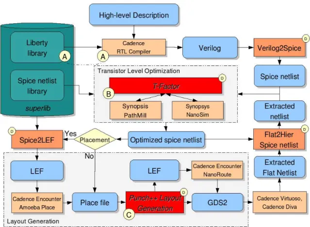
In other words, a transistor-level design current allows transistors to be sized in critical paths of the circuit while preserving other paths with minimal transistor size. First of all, the design flow is based on a database that stores each cell's structure, estimated area, timing and energy consumption.
The Super Library Generation
The Development of a superlib
The number of strengths of the superlib drive was limited by runtime and memory consumption. An example of the representation of rise and fall time in freedom format is shown in Figure 2.4(c).
The Transistor Level Design Flow
The Transistor Level Optimization
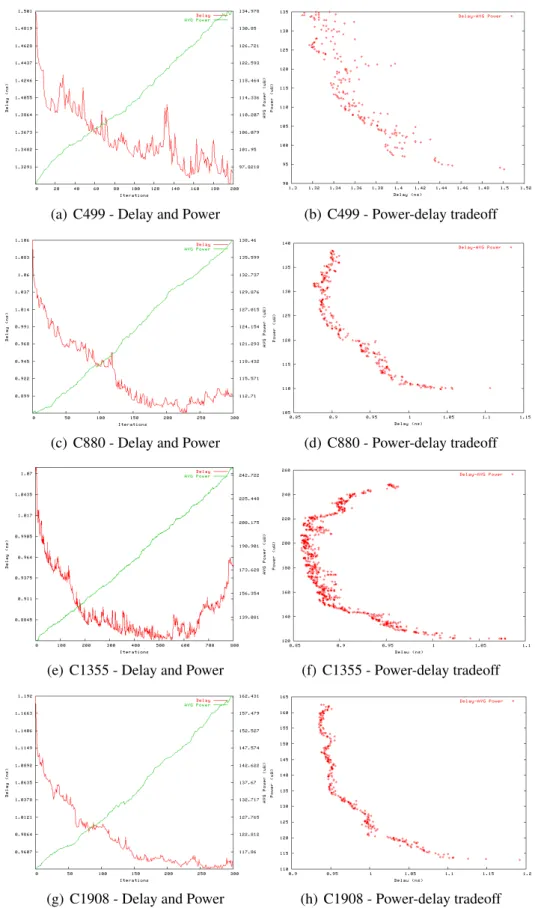
The power consumption is detected by the function getPowerInformation( N, V )(line 6) as a function of the input vector V. The occupancy factor is used to find a cell among all the sizing candidates. An important aspect is the linear growth of the energy consumption as a function of the dimensioning algorithm.
Transistor Level Optimization for Leakage Reduction
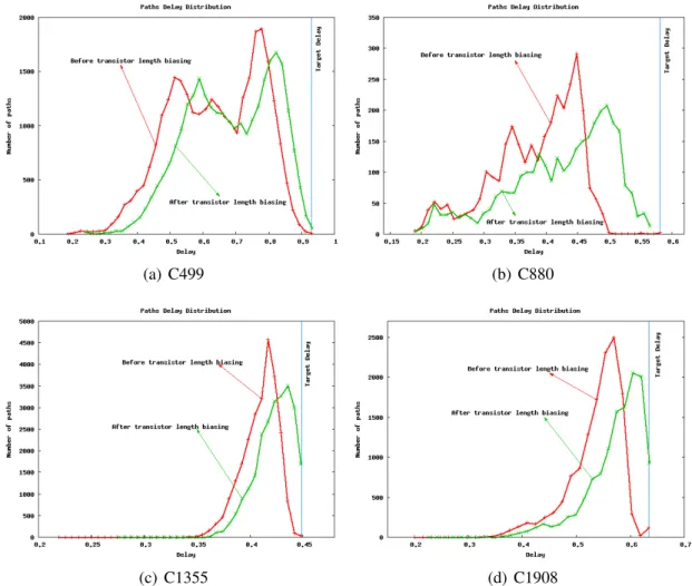
Gate length biasing consists of adjusting the length of the transistors to reduce the current leakage [GKSS04, KMS05, BCV06]. Results show that the gate length bias is very effective in reducing the current leakage.

The Transistor Level Layout Generation
FunctioncompactLayout(Lr, T) is responsible for compacting the layout and applying the technology rules to the layout. After the layout of each row is done, the circuit is routed by Cadence nanoroute [CAD07b] (Function routeCircuit(L) in line 8) and the circuit is saved in GDSII format (FunctionwriteLayout(L) in line 9).
![Figure 2.12 shows a comparison between the layout style of the tool presented in [Laz03] and the layout style of the tool developed in this work](https://thumb-eu.123doks.com/thumbv2/1bibliocom/462482.68526/42.892.136.768.302.574/figure-shows-comparison-layout-presented-laz03-layout-developed.webp)
Transistor-Level vs Traditional Design Flow Summary
A Comparison with the Traditional Standard Cell Design Flow
The design process was done on the basis of high effort to meet the minimum possible delay. We observed that this high effort resulted in the insertion of many buffers in the critical path.

Conclusion
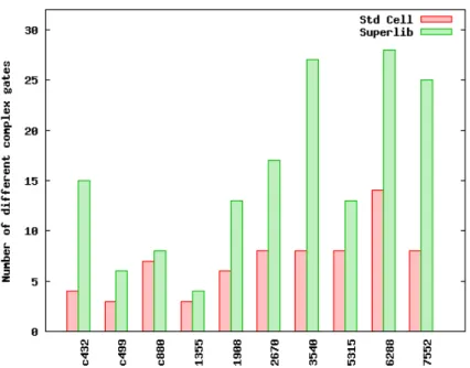
Circuit Time (ns) Total Power Consumption (uW) Std Cells Suggested Gain Std Cells Suggested Gain. These results were achieved by trying to improve layout quality regarding polysilicon and metal interconnects and by the ability to optimize the circuit for the large number of logic functions and drive strengths found in a library.
Introduction
An Overview of the Algorithm Classes
Deterministic Algorithms
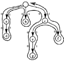
A force-oriented algorithm models a system as a graph where the position of the vertices indicates the solution. The idea of the Euler path is to walk over the graph edges where each graph edge is visited once [Wei07b]. Once the formulation converges to a solution, the result is the position of the transistors in the layout.
Stochastic Algorithms
Although the excellent properties of the linear programming, the majority of the problem cannot be represented by a linear objective function.
Goals of Placement Algorithms
The increase in resistance due to the reduction of the connection widths and the greater capacitance between lines can cause signal degradation and greater delay. To handle this limitation, placement algorithms must be able to generate balanced rows and handle empty spaces very well. A balanced distribution of cells in the rows is the key to reducing the area occupied by the circuit.
Goals of Routing Algorithms
State-of-the-art Algorithms for transistor placement and routing
Transistor Placement Using an O-tree Algorithm
To simplify the algorithm, the insertion positions are considered only at the outer nodes of the tree. In Figure 3.8(a) an example of symmetrical placement is illustrated, where the pair of transistors (B,H) and (E,F) are symmetrically placed. The mechanism to support this simultaneous optimization is the placement of transistor sub-chains, diffusion break-free components in the full transistor chains.
A Maze Routing Steiner Tree with Effective Critical Sink Optimization
It is important to note that the three horizontal routing traces in the two-dimensional layout are divided into the two-dimensional layout. Of the various topologies generated, the one with better critical path isolation failed to provide a good wire length for the rest of the tree. The AMAZE algorithm outperformed algorithms used in industry and state-of-the-art academic research, such as AHHK by 25%-40% and P-Trees by 1%-30%.
Routing with a Negotiation-based Algorithm
To obtain better electrical properties of the resulting cell layout, different weights are applied to the edges of the graph according to its layer and position. This enables an area reduction if no gates are placed in the closest track to the transistors. For this reason, better area results are obtained when the routing cost of the graph edges leading to these ports is increased.
Transistor Placement Technique Using Genetic Algorithm And Analyt-
- Initial Population Generation
- The Placement Parameters
- The Mathematical Modeling
- Obtained Results
The function doEvolution( P ) is basically the reproduction of the chromosomes in the population to generate a new population with better results. The aim of the proposed technique is to reduce the wire length connecting the transistors. The wire length of a connection was calculated by the coordinates of the points of a net in the matrixeQxenQy.
Compaction and Layout Optimization using Linear Programming
Once the relative position of the polygons is known, it is possible to describe the relationship between these polygons as linear programming. The distance between two transistors should be as small as possible to reduce the area and perimeter of the transistors drain/source. For example, the distance between stacked transistors is very important because of the resistance of a transistor's active region.
Overview of the Algorithms Developed in the Punch++
Each of the aspects shown in Algorithm 6 can be considered in linear programming by applying costs to the constraints and inserting them into the objective function. Therefore, to improve the quality of the layout, the objective function can be written as. After that, the formulations are solved in Function callLPSolver( D ) and FunctionplacePolygons( L ) places each polygon in the layout.
Conclusion
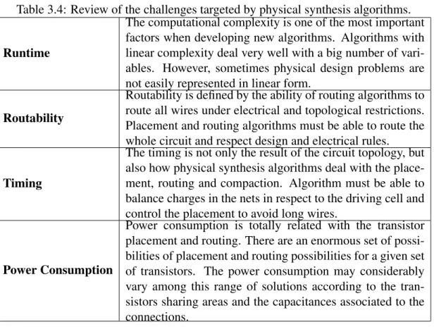
Placement and routing algorithms must be able to drive the entire circuit and respect design and electrical rules. Timing is not only a result of circuit topology, but also how physical synthesis algorithms deal with placement, routing, and compression. The algorithm must be able to balance the loads on the grids with respect to the moving cell and control the placement to avoid long wires.
Introduction
The offset between the Earth's geographic and magnetic axis causes an asymmetry in the radiation belt over the Atlantic Ocean off the coast of Brazil, allowing the inner belt to reach a minimum altitude of 250 km. The total ionizing dose (TID) is the result of breakdown due to the cumulative energy deposited in the material. Unlike TID and DD, single event effects (SEE) occur when a single ion strikes a material with enough energy in a device to cause system failure.
Single Event Effects (SEEs)
Soft SEE
A single heavy ion striking a silicon device loses its energy as a result of the production of free electron-hole pairs. LET is a measure of the energy transferred to the material as a function of an ionizing particle passing through it. Schematic of the latch is shown in Figure 4.6(a), which is composed of two inverters and two transmission gates controlled by the clock signal.
![Figure 4.4: The current curve as result of a α-particle striking a device according [Mes82].](https://thumb-eu.123doks.com/thumbv2/1bibliocom/462482.68526/77.892.223.660.558.882/figure-current-result-particle-striking-device-according-mes82.webp)
Single Hard Errors (SHE)
When the internal node voltage reaches VDD2, the converters force the latch to change its state and a bit reversal occurs. Additional details on the characterization of this type of memory error are presented in [DGC+92, PCBO94].
Other Radiation-Induced Effects
Conclusion
The main idea in the spatial replication is that a particle hitting one of the elements does not affect the others. The outputs of the replicated elements are thus compared and the filtered signal is propagated. This chapter presents some state-of-the-art techniques for mitigating the effects of single events in sequential and combinational circuits.
The Classic Techniques
The Figure 5.2 shows two implementations of the TMR technique targeting disturbance tolerance for combinational and sequential blocks. In the first implementation (Figure 5.2(a)), the clock signal of each flip-flop (CLK,CLK+δandCLK+ 2×δ) is delayed so that the input signal is captured at three different instants. The same idea is used in Figure 5.2(b), where the same clock signal is used in the tree Flip-Flops, but the input signal is delayed by Delay Blocks.
Gate Duplication Methods
The time penalty of these TMR techniques over the time of a D-Flipflop is 2×δ+TDelayV oter. The TMR is usually applied to sequential elements, but it can be used on combinational blocks and an entire circuit, but they present a very high overhead in area (more than 200%). Furthermore, techniques that modify clock signal as shown in Figure 5.2(a) can present additional and usually unnecessary design challenges due to clock skew and clock tree propagation.
Gate Sizing Techniques
Protecting Sequential Elements Through Feedback Control
Using Time Redundancy To Protect Sequential Elements
The delay block must be able to degrade the signal at the input of the CWSP cell according to the transient fault time that we manage to tolerate. A case study is made to verify the penalties of CWSP cell insertion in a MIPS-like processor and an 8051 controller. The TMR overhead is constant in the 250ps and 500ps error implementations because we assume that the delay blocks are shared with any D-FlipFlop.

Conclusion
TMR works when the single event only occurs in one element, independent of the particle energy. The technique does not add additional complexity to the clock synthesis, but increases the clock period by 2×δ. A block with delayδ must guarantee that only one transient pulse arrives in one of the inputs.

Introduction
Combinational Circuits Sensitivity
The Logical Masking
In other words, the pulse is masked as a function of the vector applied to the primary inputs (PI) of the circuit. The controllability of the gate output node is obtained by the gate logic function as shown in Table A.7 [JJ05]. A pulse in one of the gate inputs propagates through the gate only if an uncontrolled value is applied to the other input.
The Electrical Masking
In an OR gate, the same situation is considered where the impulse propagates through the gate only if the non-controlling value is applied to the other input.
An Analytical Model for Single Event Transients
Modeling Resistances and Capacitances
Suppose NMOS transistors are "ON" in the NAND gate of the example due to input signals = "1" and b = "1". Cconnect is the wiring and parasitic capacitances, and Cgateg2 is the gate capacitance of all transistors connected to the output node. These analytical equations allow to model the behavior of the transient pulse as a function of the electrical properties of the devices.
The Single Event Transients Model
The models presented in [WVK07] are derivatives of the double exponential to obtain peak time peak and peak voltage. This differential equation (A.2) can be solved to obtain the voltage V(t) at the struck node. The voltage starts to decrease exponentially after the peak. 6.11) Equation (A.11) shows the transient duration of the pulseτn, where the second term corresponds to the analytical solution if the time RC is much greater than τα and the last term corresponds to the analytical solution if the time is much greater than tanRC.
Single Event Transient Propagation
Second and third cases are related to a partial degradation of the transient pulse according to the relationship with the SET duration τ and the gate delay τg. These properties can also be useful to obtain the maximum acceptable transient pulse duration in a node. An important note is that a transient pulse does not need to be attenuated in the mains (except in cases where gates are connected to outputs).
The Transistor Sizing Strategy
We consider the maximum acceptable transient pulse in a node as the maximum SET duration that is attenuated before the primary outputs. When gate transistors increase in size, the delay usually decreases and a transient pulse propagates with less degradation. Misinterpretation regarding SET propagation must occur if the transient pulse is evaluated before sizing the gates in the path to the POs.
The Transistor Sizing Model
A node is assumed to be electrically masked if the transient pulse is suppressed before the outputs. The transient pulse propagation equations in Section A.4.2.3 address four situations where the SET duration can be fully reduced, partially reduced, or expanded. The function sizeTransistors( s, g, τn ) finds the minimum width of the transistors for the gateg according to the duration of the transient pulse τn.

Results
The worst case was an 87% area overhead for complete protection (0% sensitivity) against particles with charge Q = 0.3pC. Results show an average 83% area overhead for the symmetric size and 61% for the asymmetric size. Results show area overhead and timing penalties to protect some circuits from particles with charge Q= 0.3pC with final sensitivity of 0%.

Conclusions
La réduction de la puissance dynamique est le résultat direct de l’optimisation de la taille des transistors. La Figure A.5 montre la puissance et le retard résultant de la première étape d'optimisation pour certains circuits. Pour cette raison, nous incluons l’ajustement de la longueur des transistors dans le flux de conception.
Les résultats concernant l'ajustement de la longueur des transistors sont présentés dans le Tableau A.1. Une méthode de propagation est utilisée, dans laquelle le retard de porte et la durée d'un transitoire sont estimés.
![Figure A.1: retard des portes et des interconnexion versus les génération de technologie [SIA97]](https://thumb-eu.123doks.com/thumbv2/1bibliocom/462482.68526/118.892.197.691.669.1030/figure-retard-portes-interconnexion-versus-génération-technologie-sia97.webp)
![Figure 1.1: Gate and interconnect delay versus technology generation [SIA97]. Delays for feature size below 100nm is estimated.](https://thumb-eu.123doks.com/thumbv2/1bibliocom/462482.68526/20.892.195.690.571.928/figure-interconnect-versus-technology-generation-delays-feature-estimated.webp)
![Figure 1.3: Clock frequency of high performance ASIC and custom processors in differ- differ-ent process technologies [CK02].](https://thumb-eu.123doks.com/thumbv2/1bibliocom/462482.68526/22.892.196.687.277.642/figure-clock-frequency-performance-custom-processors-process-technologies.webp)
![Figure 2.2: Runtime and occupied memory as a function of the number of gates in a library [CAD07a].](https://thumb-eu.123doks.com/thumbv2/1bibliocom/462482.68526/29.892.223.672.152.485/figure-runtime-occupied-memory-function-number-library-cad07a.webp)