Umesh Mardolcar pela ajuda e contribuição, ao longo do meu trabalho de tese, nas medições de espectroscopia de admissão e na montagem do sistema de vácuo. Nanofios de óxido de zinco têm sido usados para melhorar a eficiência da coleta de portadores de carga em células solares sensibilizadas por corante (DSSC), pois fornecem um caminho direto para o ânodo. Nanofios de óxido de zinco, com 100 nm de espessura e 5 µm de altura, foram depositados por processo químico úmido e suas propriedades elétricas foram estudadas e comparadas com uma amostra de filme fino, onde o objetivo principal foi estudar os efeitos de superfície devido à adsorção de moléculas.
Palavras-chave: Oxido de Zinco, Nanofios, Defeitos profundos,´ Trap-Filled-Limit, Efeitos de Superf´ıcie. Strong variations of the power law exponent as a function of the applied electric field in log-log representations of current-voltage characteristics are interpreted as a manifestation of transport in the trap-filled limit regime, leading to an estimate of the density of deep trap states aspt cm−3 and the concentration of carriers to ben cm−3.
List of Tables
List of Abbreviations
Introduction
Focusing on ZnO 1D structures, the piezoelectric properties of these nanostructures were investigated for their application in nanoelectromechanical systems such as piezoelectric energy harvesters. Another very interesting application that has been reported is in so-called piezotronics, which is the use of the properties of piezoelectricity to create a transistor. A possible configuration is that the nanowire voltage acts as the gate voltage in the MOSFET transistor [4, 5].
Furthermore, with regard to optical properties, it has been reported that arrays of nanowires have been used as light-emitting diodes[3], and it has been shown that limiting the quantum size increases the exciton binding energy, which as previously stated, increases efficiency. of emission. However, most work has focused on comparing surface-related effects in homogeneous ZnO thin films with those observed in nanowire structures.
Literature Review
- Properties of Semiconductors
- Defects and Impurities
- Carrier Transport Properties
- Current Injection
- Piezoelectric Properties
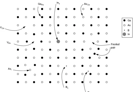
The main purpose of this process is to change and control the conductivity of the material. The localized states near one of the bands are shallow traps, which are usually the goal when doping the material. Therefore, depending on the position of the state, a certain process of either capture or emission will be dominant [7, 8].
It should be noted that this result only holds for small magnitudes of the electric field and will not be discussed further. Such a gradient will create a net movement of carriers, from regions of high concentration to regions of low concentration. A simple way to deal with this is to add a negative term on the right-hand side of equation 2.29,−δρτ, where δρ is the excess carrier concentration and τ is the recombination lifetime.
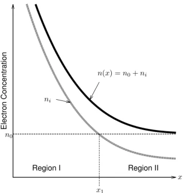
This experiment involves illuminating a semiconductor with a light pulse and studying the behavior of excess carriers created under an electric field. These last two approximations face some validity problems in the vicinity of the contacts, where the diffusion current has some contribution due to the spatial variation of the electron concentration from the contact to the insulator. Therefore, on the right side of the equation, we only have the excess charge concentration, or the charge that was injected into the material and therefore not neutralized.
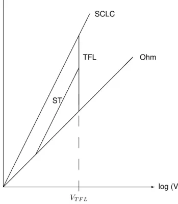
Phenomenologically, the following behavior of the current-voltage curve is expected for a single set of traps. And it can be shown that this current increase after an individual series of traps is filled is almost vertical, which is one of the most remarkable results of this theory, because experimentally such a high slope in the current-voltage curve can be misinterpreted as an electrical defect in the material. As a result, there is a fourth regime intermediate between Ohm's law and the TFL regime, the so-called shallow trap (ST) regime, which exhibits a quadratic dependence on the voltage, like the SCLC.
Besides that, it also affects the slope of the TFL regime, which is steeper for higher values of A. The main achievement of this theory is the prediction of the TFL regime, as well as the voltage at which it starts, VT F L (Eq. . 2.58).
Zinc Oxide
- Basic Properties
- Optical Properties
- Piezoelectricity and Energy Harvesting
- Description of the Samples
- Nanowires Fabrication Method
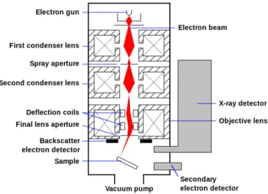
- Scanning Electron Microscope (SEM)
- Photocurrent Spectroscopy
- Current-Voltage Characteristics
- Transient Photocurrent
- Admittance Spectroscopy
Therefore, it is more likely that hydrogen impurities are the source of unintentional n-type doping. In addition, deep donors, which are not responsible for n-type behavior, will compensate for p-type doping. In addition, this effect also provides a blue shift of the emission in the photoluminescence (PL) spectrum [13].
These mentioned defects are thus the most likely cause of the broad emission, which is in agreement with the literature. One of the most important properties of ZnO is certainly its piezoelectricity, which arises from the non-central symmetric structure. The difference is whether the device is designed to absorb energy through axial compression of the nanowires or by bending them.
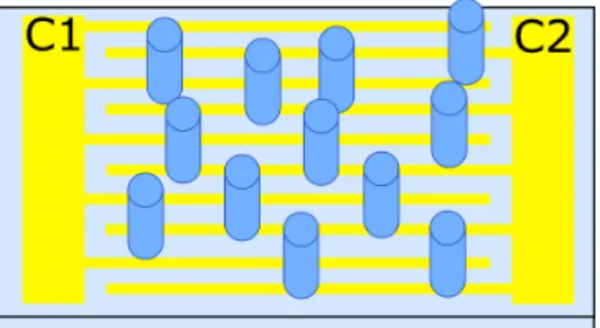
First, the height of the nanowires is not uniform, so they are not all actively producing electricity. One proposed solution to the latter problem is to place insulating polymers in the nanowire spacing. A schematic representation of these patterns is shown in Figure 3.5, which illustrates a layer of nanowires on top of gold interdigital contacts.
This last step will promote the growth of the seed layer through the thermal decomposition of the zinc acetate. Thus, by performing a fit to the absorption coefficient with this expression, which is known as Tauc plot, the value of the band gap Eg is determined. To investigate the optical properties of the structures, especially the band gap Eg and Urbach energyEu, photocurrent spectrum was obtained using the experimental setup illustrated in Figure 4.2.
Results and Discussion
- Scanning Electron Microscope (SEM)
- Energy Harvesting
- Photocurrent Spectroscopy
- Current-Voltage Characteristics
- Transient Photocurrent
- Admittance Spectroscopy
These regions, possibly due to some impurities in the substrate during the growth process, may be another reason for the different resistance compared to the other three samples. The displacement vector can also be written as: where Ezpis the electric field due to the piezoelectric effect. For the bending configuration, the root end of the nanowire is fixed, while the other end is pushed by a lateral force.
In figure 5.7, the photocurrent spectrum of PS1, PS2 and PS3 is shown, where the ratio between the photocurrent and the dark current is represented. The results for the PS3 are presented in figure 5.9, where several IV curves were obtained at different temperatures. For higher voltages, the sample shows high slopes, which are characteristic of the TFL regime.
Regarding the thin film, MEFT4, the IV curves obtained are in Figure 5.11, where the sample is always behaved as ohmic. In the dark, oxygen is adsorbed on ZnO surface defects by capturing electrons, which is illustrated in solid lines in Figure 5.13. This effect, due to the larger surface-to-volume ratio, is more important for nanowires than for thin films.
Each peak can be associated with the adsorption of two different molecules, or with two possible lattice sites where the same molecule can form a chemical bond. The decay curves over time are in Figure 5.15 and the result from the Laplace Transform Method in Figure 5.16. This can be explained by the fact that nanowires have a larger surface-to-volume ratio than a thin film, being able to accommodate more adsorbed molecules.
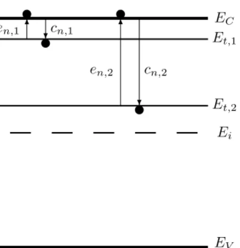
However, the first one may be an artifact due to the limitation of the analyzer at low frequencies, and this "jump" in capacitance may be the point where the device begins to read correctly. Figure 5.24 shows all four trap states identified in this work by transient photocurrent and admittance spectroscopy, in their respective locations within the band gap.
Summary and future work
Thus, this shift in temperature where the sample changes its behavior may be due to the variations in the air composition, such as humidity. Furthermore, TPC suggested a higher increase in pt,0 than was observed in IV curves, recalling that VT FL is proportional to pt,0. Consequently, it is proposed as a future work to perform these experiments in a controlled ambient atmosphere as well as in vacuum in the case of IV characterization and transient photocurrent.
This would answer the question just mentioned and the question raised by the TPC about the origin of the two peaks. A similar approach was used in [30], where the persistent photoconductivity (or PPC effect) of a single ZnO nanowire was investigated as a function of the surrounding atmosphere. However, only the decay rates were examined in this publication, but not the density of states associated with the decay.
Regarding the ability of these samples as energy harvesters, we presented a model and simulation results of the stress produced by a single nanowire when compressed or bent.
Bibliography
Room temperature photoluminescence and photoconductivity of wet chemically deposited ZnO nanowires used for solar cells. Improved Laplace transform method for determining trap densities from transients: application to ZnO and films. A study of the density of hole states in amorphous semiconductors from thermostimulated conductivity spectra. Applied physics A.
Theory of isothermal currents and the direct determination of step parameters in semiconductors and insulators containing arbitrary step distributions. Density of band gap traps in polycrystalline films from photoconductor transients using an improved Laplace transform method. Distinction between bulk and interface states in CuInSe[sub 2]/CdS/ZnO by space charge spectroscopy.
Determination of defect distributions from admittance measurements and application to Cu(In,Ga)Se2 based heterojunctions.
Appendix A
Vacuum System
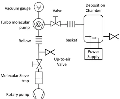
The proposed scheme is on figure A.2, where one valve, two up-to-air valves and a T-connector have been added. This will allow one to ventilate just the room or just the pump line, and keep the vacuum in the other part. Another advantage is that it allows a safer shutdown of the turbo molecular pump by separating it from the pre-vacuum pump, which reduces the risk of oil contamination of the pre-vacuum pump since while the turbo molecular is slowly shutting down, it is at lower pressure.
Appendix B
Communication with Impedance Analyser
![Table 3.1: Physical properties of wurtzite ZnO (values at T = 300 K) [1].](https://thumb-eu.123doks.com/thumbv2/123dok_br/19768770.0/39.892.190.660.109.689/table-physical-properties-of-wurtzite-zno-values-300.webp)
![Figure 3.4: The two setups of piezoelectric generators from [3].In compression configuration, the nanowires are in between two conductive layers, where the top one compresses the nanowires.](https://thumb-eu.123doks.com/thumbv2/123dok_br/19768770.0/41.892.130.783.238.469/piezoelectric-generators-compression-configuration-nanowires-conductive-compresses-nanowires.webp)