www.adv-radio-sci.net/9/241/2011/ doi:10.5194/ars-9-241-2011
© Author(s) 2011. CC Attribution 3.0 License.
Radio Science
A low power clock generator with adaptive inter-phase charge
balancing for variability compensation in 40-nm CMOS
U. Schulze, M. Broich, O. Weiss, and T. G. Noll
Chair of Electrical Engineering and Computer Systems, RWTH Aachen University, Germany
Abstract. Power dissipation besides chip area is still one
main optimization issue in high performance CMOS design. Regarding high throughput building blocks for digital sig-nal processing architectures which are optimized down to the physical level a complementary two-phase clocking scheme (CTPC) is often advantageous concerning ATE-efficiency. The clock system dissipates a significant part of overall power up to more than 50% in some applications.
One efficient power saving strategy for CTPC signal gen-eration is the charge balancing technique. To achieve high efficiency with this approach a careful optimization of tim-ing relations within the control is inevitable.
However, as in modern CMOS processes device variations increase, timing relations between sensitive control signals can be affected seriously. In order to compensate for the in-fluence of global and local variations in this work, an adap-tive control system for charge balancing in a CTPC gener-ator is presented. An adjustment for the degree of charge recycling is performed in each clock cycle. In the case of in-sufficient recycling the delay elements which define duration and timing position of the recycling pulse are corrected by switchable timing units.
In a benchmark with the conventional clock generation system, a power reduction gain of up to 24.7% could be achieved. This means saving in power of more than 12% for a complete number-crunching building block.
1 Introduction
Designing high performance building blocks for digital sig-nal processing systems is facing increased challenges in modern CMOS generations especially concerning leakage and process parameter variation (Pang et al., 2009; Das et al., 2009; Nassif et al., 2007; Jaffari and Anis, 2006). These challenges of ultra deep submicron technologies have a great impact on well established design strategies. Nevertheless
Correspondence to:U. Schulze ([email protected])
the demand of efficient implementations concerning area, throughput and power dissipation has to be satisfied.
For highly pipelined architectures in many cases a com-plementary two-phase clocking scheme (CTPC) is the most efficient choice for realizing the synchronization. In such building blocks power dissipation of the logic can often be reduced to 60%, in some applications even down to 50% of overall power (see Fig. 1, left diagram) This makes the clock system to be the main energy consumer.
In order to reduce clock power an approach for signal gen-eration which performs charge balancing between comple-mentary phases is very promising (Noll and de Man, 1992; Kyriakis-Bitzaros and Nikolaidis, 1997). With this strategy the power efficiency in the clock system can be be enhanced by one third (Fig. 1, right diagram). For a proper function-ality of the charge balancing technique, the control signals for buffers and balancing transistors have to be in well ad-justed timing relations to each other. Even small shifts be-tween the signals can reduce the amount of recycled charge significantly or cause shorts towards the power supply. As in modern CMOS technologies process variations increase and will in future generations increase even more, power saving clock signal generation will become more complicated.
To overcome the difficulty of timing shifts between sensi-tive control signals caused by variability we propose in this work an adaptive approach. In a first step, the quality of the charge balancing event is evaluated. If it is not working well timing relations between the control signals are corrected by inserting or skipping little delays resulting in an optimized adjustment of the signals and thus in optimum recycling per-formance.
Fig. 1.Power breakdown of FIR-filter with/-out charge balancing.
2 Inter-phase charge balancing: basic principle
The mechanism of charge balancing between two comple-mentary phases of one clock signal has been introduced in Noll and de Man (1992). Figure 2 shows the basic circuit in-cluding two capacitors which represent the capacitive loads of both complementary signals8and8. The parasitic el-ements include capacitances of global and local wiring and the clock inputs of all pipeline elements.
Shorting both phases at the moment of attended switching will equalize the charges on both parasitic capacitors. The voltage equilibrium can thus be reached without taking any current from the supply nodes in a best case. If the hardware overhead for the charge balancing circuits is neglected about 50% of power saving within the clock network is possible.
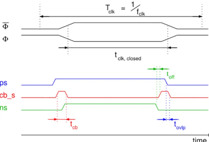
In Fig. 3 both complementary phases8and8of one clock signal within a CTPC system and the according control sig-nals are illustrated. The balancing mechanism works as fol-lows: to initiate a clock signal transition at first, both tri-state buffers have to be closed making the clock trees floating for a short amount of timetoff(see Fig. 3, control signalspsand
ns).
After that, the charge balancing transistor is opened with a balancing pulse of lengthtcb(see Fig. 3, control signalcb s) until the equilibrium is almost reached.
Finally, with a little, well adjusted overlapping timetovlp (see Fig. 3, control signalsns andps) two of the four tri-state transistors get an impulse to conduct for the rest of the half-cycle. This event will complete the transition.
The optimal choice oftovlp results in a fast clock signal transition without any short-circuit currents. During this time the charge balancing transistor begins to close while the tri-state buffers already start conducting increasing the risk of aVDD-to-GNDshort. In modern CMOS technologies this overlap time has to be reduced or eliminated in order to get good robustness against process variations.
3 Two kinds of signal degradations and the reasons
In the case of well adjusted charge balancing thecb spulse in Fig. 3 is as long as necessary to recycle about half of the
cb_s
charge balancing tri−state buffer
ps
ns
tri−state buffer
Cφ Cφ
transistor
ns
ps
Fig. 2.Charge balancing circuit for complementary clock phases.
tcb t
ps
cb_s
ns
ovlp
t off
tclk, closed
time
Φ
Φ
clk
T = 1f
clk
Fig. 3.Timing of control pulses and resulting clock signal phases.
charge which is stored in the clock capacitances. This leads to the best power-delay efficiency, because the clock tran-sition time is as short as possible at the maximum recycled charge.
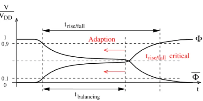
When the balancing time is shortened, for example due to a slower path for the event that activates the balancing tran-sistor, the full power saving potential cannot be exploited. A clock signal waveform as illustrated in Fig. 4 will be the result. In this case the power gain towards a conventional clock system decreases. But the timing constraints for the clock transitions are fulfilled and the functionality of the log-ical paths in the building block is guaranteed.
An opposite situation will occur when the balancing im-pulse gets too long due to signal run time degradations re-verse to the case explained above. The resulting waveforms are shown in Fig. 5. In this case the power gain is marginally increased. However, the functionality of the system cannot be guaranteed any longer, because clock transitions get very long which may cause timing violations for critical paths in the logic.
t V
0,9 1
0.1 0
t
t
Adaption
P criticalv
Φ Φ
balancing DD
V
rise/fall
Fig. 4.Charge balancing time is too short.
VDD V
tbalancing 0,9
1
0.1 0
t
Adaption rise/fall
t Φ
Φ t criticalrise/fall
Fig. 5.Charge balancing time is too long.
4 Adapting the charge balancing time
To overcome the above described drawbacks we propose in this work a clock generator which is able to adapt the pro-cess of charge balancing individually for every produced chip over the relevant temperature range and in a wide interval of supply voltages. For the adaption functionality it is inevitable to fulfill some kind of measurement towards the recycling event.
As quantification of the recycled charge is complicated to realize we developed a circuit which allows an observation of the charge balancing process.
4.1 Equilibrium detection gate
With a simple binary information, if a voltage level near the equilibrium has been reached before the tri-state buffers are activated, an adaption decision can be made.
Figure 6 shows the new gate which is able to make a full-swing transition while both inputs, which are the comple-mentary clock phases8and8, reach only a level of half the supply voltage – the equilibrium.
Suppose a rising transition of clock signal 8. At the beginning input8=1 and input 8=0. From this it fol-lows that both n-transistors on the left side conduct, because their gates are connected to 8. Both left outputs are on logical “0”. Accordingly the outputs on the right side are both on logical “1”.
Fig. 6.Equilibrium detection gate.
When8is falling untilU8−U8≈Vthall four transistors in the middle of the gate, the devices which have no connec-tion toVDDorGNDget closed. When8is reaching a volt-age level ofU8=VDD−Vththe upper left p-transistor be-gins to conduct pulling the green equilibrium detection signal ed(8)toVDD. Analoguous the other green outputedn(8) on the lower right position of the gate is pulled down toGND. These synchronous switching events mark the detection point for the equilibrium.
Later on, whenU8−U8≈ −Vth the blue output signals ed(8)and edn(8)begin to switch. These events are not relevant for the detection of a rising edge of8as explained above. ed(8)andedn(8)can in the following half-cycle detect the equilibrium of a rising edge of8.
4.2 Timing relation for the equilibrium detection
A detection of the equilibrium is not enough to make a deci-sion if the balancing process is well adjusted or not. To get an information about the quality of the charge recycling it is important at what time the equilibrium is reached.
For this purpose a capture flip-flop is required which has to be clocked by the control signal of the according tri-state buffer. When the tri-state buffer is activated the balancing event ends and from then on charge is taken from the power supply. At this moment the voltage equilibrium should be reached if the balancing process is properly adjusted.
Therefore the capture flip-flop is closed by the tri-state ac-tivation signal (see Fig. 7). If the equilibrium detection signal comes too late it cannot enter into the capture flip-flop. The output of the flip-flop remains on logical “0” and gives the message: “balancing time is too short”.
In this case the balancing impulse will be made a little longer by inserting more delay elements1t into the timing path for the charge balancing impulse and for the tri-state enable signal.
tri−state enable
capture flip−flop
4−bit shift register
shift left = "make balancing impulse shorter" shift right = "make balancing impulse longer"
∆ ∆ ∆
1 t 2 t 4 t 7∆t
charge balancing impulse delay multiplexer
every 16 cycles one impulse
equilibrium detected
Fig. 7.Charge balancing adaption logic.
shortening was not necessary it is corrected in the following cycle by the adaption mechanism explained above.
5 VLSI implementation of the clock generator with
parameter adaption
With the above described logic path the clock generator with parameter adaption has been implemented. For the realiza-tion in a 40-nm CMOS technology there are some further details to regard.
In order to obtain an efficient implementation a trade-off between hardware complexity and timing shift granularity has to be found. Therefore, we decided not to add the same delay increment1t with every step of the delay multiplexer. For a small balancing time the increment towards the next longer one is chosen small, while the increment is gradu-ally increased with longer balancing times. With this non-equidistant delay steps an overall number of four different delays is sufficient (see Fig. 7).
For a robust functionality of the system steep transitions of the equilibrium detection signals are important. On the one hand, this can be enhanced by high threshold voltage devices for the four middle transistors in Fig. 6 which are not con-nected toVDDorGND. The higher their threshold voltage is the earlier they are switched off when a clock transition occurs and the outputs of the detection gate are earlier pre-pared for switching. On the other hand, the four transistors connected toVDDorGNDare low threshold voltage devices for fast switching in the moment the equilibrium is reached.
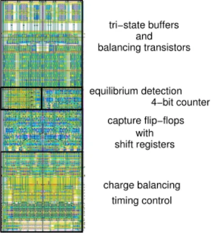
Figure 8 shows the layout of the 40-nm CMOS implemen-tation of the clock generator. The adaption circuitry, posi-tioned in the middle, accounts for about 30% of the com-plete area. As the clock generator usually consumes much less than 5% of the chip area of a signal processing build-ing block, the overhead for the parameter adaption feature is almost negligible.
equilibrium detection and
with
charge balancing timing control capture flip−flops
shift registers balancing transistors
tri−state buffers
4−bit counter
Fig. 8.Layout of the clock generator in 40-nm CMOS.
Table 1.Power dissipation @400 MHz; 40◦C; 650 mV.
Corner case fixed adaptive .gain.
charge balancing charge balancing
Slow 558 µW 584 µW −4.5%
Typical 774 µW 627 µW 19%
Fast 948 µW 714 µW 24.7%
6 Benchmarking
In this section we will compare a conventional clock gen-erator and one with charge balancing but without parameter adaption to the proposed new clock generator with parameter adaption for the charge balancing feature.
In Table 1 the power dissipation of both charge balancing implementations is summarized for the classical process cor-ners at a total clock capacitance of 4×C8withC8=1 pF.
One drawback of the system without parameter adaption is, that the fixed timing for the balancing pulses has to be a compromise over all corner cases. The adaptive system switches into another delay multiplexer position for each of the three corner cases. In the slow-corner, for which the fre-quency constraint of the application has to be met, the con-ventional system is optimized and has a small advantage over the adaptive system. But in the typical- and fast-corner the power efficiency of the adaptive system is by about 20% su-perior.
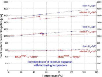
In Fig. 9 the power dissipation of both clock systems is il-lustrated over the relevant temperature interval for three dif-ferent capacitive loads of a clock tree at slow/650 mV.
Fig. 9.Power dissipation over the relevant temperature interval.
Table 2.Clock power: Slow-corner vs. Monte Carlo simulation.
Corner case no fixed adaptive
.charge bal.. .charge bal.. .charge bal..
Slow 719 µW 558 µW 584 µW
gain – 23% 19%
Monte Carlo 746 µW 705 µW 659 µW
Global: slow
gain – 5% 11%
Finally, a monte-carlo benchmark is presented in Table 1 over all three clock systems mentioned above. The clock sys-tem with fixed charge balancing suffers much from device variations. A worst scenario taken from monte-carlo simula-tions reduces the gain towards the conventional clock system by more than three-quarters. To some extent the adaption logic is able to compensate these degradations. The resulting gain of the adaptive approach is more than twice as high as without parameter adaption.
7 Conclusion
In a clock system with complementary phases the power dis-sipation can be reduced by about 30% with the implementa-tion of a charge balancing approach. One drawback of this approch, the compromise which has to be made for the bal-ancing time over all process corners can be very good com-pensated by an adaption logic. The adaptive clock generator proposed in this work has an about 20% lower power dissi-pation in the typical- and fast-corner towards the same clock generator without adaption feature. This means a total power reduction within a high performance number-crunching unit of more than 10%.
Verifying the clock system with monte carlo-simulation reveals, that a charge balancing approach suffers much from process variation. The gain towards a conventional clock sys-tem can be more than doubled by applying a parameter adap-tion to the charge balancing mechanism.
For future research an alternative adaption logic may be possible by using an equilibrium detection gate based on a short circuit measurement.
References
Das, B. P., Amrutur, B., Jamadagni, H. S., Arvind, N. V., and Vis-vanathan, V.: Within-Die Gate Delay Variability Measurement Using Reconfigurable Ring Oscillators, IEEE Transactions on Semiconductor Manufacturing, 22, 256–267, 2009.
Kyriakis-Bitzaros, E. D. and Nikolaidis, S.: Design of Low Power CMOS Drivers Based on Charge Recycling Technique, IEEE Symposium on Circuits and Systems, pp. 1924–1927, 1997. Jaffari, J. and Anis, M.: Variability-Aware Device Optimization
un-der Ionand Leakage Current Constraints, International Sympo-sium on Low Power Electronics and Design, 2006.
Pang, L.-T., Qian, K., Spanos, C. J., and Nikolic, B.: Measurement and Analysis of Variability in 45 nm Strained-Si CMOS Technol-ogy, IEEE Journal of Solid-State Circuits, 44, 2233–2243, 2009. Nassif, S., Bernstein, K., Frank, D. J., Gattiker, A., Haensch, W., Ji, B. L., Nowak, E., Pearson, D., and Rohrer, N. J.: High Performance CMOS Variability in the 65 nm Regime and Be-yond, IEEE International Electron Devices Meeting, pp. 569– 571, 2007.