Vol. 4 No 2, 02004(5pp) (2012) Том 4 № 2, 02004(5cc) (2012)
2077-6772/2012/4(2)02004(5) 02004-1 2012 Sumy State University
Design and Implementation of a Hybrid SET-CMOS Based Sequential Circuits
Anindya Jana1,*, Rajatsuvra Halder1, J.K. Sing2, Subir Kumar Sarkar1,†
1 Department of Electronics & Telecommunication Engineering, Jadavpur University, Kolkata-700032, India
2 Department of Computer Science and Engineering, Jadavpur University, Kolkata-700032, India
(Received 05 December 2012; revised manuscript received 24 April 2012; published online 07 May 2012)
Single Electron Transistor is a hot cake in the present research area of VLSI design and Microelectron-ics technology. It operates through one-by-one tunneling of electrons through the channel, utilizing the Coulomb blockade Phenomenon. Due to nanoscale feature size, ultralow power dissipation, and unique Coulomb blockade oscillation characteristics it may replace Field Effect Transistor FET). SET is very much advantageous than CMOS in few points. And in few points CMOS is advantageous than SET. So it has been seen that Combination of SET and CMOS is very much effective in the nanoscale, low power VLSI circuits. This paper has given a idea to make different sequential circuits using the Hybrid SET-CMOS. The MIB model for SET and BSIM4 model for CMOS are used. The operations of the proposed circuits are verified in Tanner environment. The performances of CMOS and Hybrid SET-CMOS based circuits are compared. The hybrid SET-CMOS circuit is found to consume lesser power than the CMOS based circuit. Further it is established that hybrid SET-CMOS based circuit is much faster compared to CMOS based circuit.
Keywords: Single Electron Transistor, CMOS, Hybrid CMOS-SET Circuits, MIB, T-Spice.
PACS numbers: 85.35.G, 85.30.T
______________
* [email protected] † [email protected]
1. INTRODUCTION
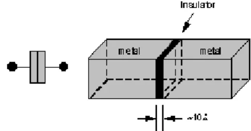
For the improvement of the VLSI devices a new strategy was taken, that is the downscaling of the de-vices. However, there have been reports suggesting that the MOS transistor cannot shrink beyond certain limits said by its operating principle [1]. Over recent years this realization has led to exploration of possible successor technologies with greater scaling potential such as single electron device technology. Single Elec-tron Device (SED) Technology is the most promising future technology to meet the demand for increase in density, performance and decrease in power dissipation in future VLSI circuits. The Single Electron devices have potential to manipulate electrons on the level of elementary charge, are thus considered to be the devic-es that will allow such a charge. In addition to their low- power nature, the operation of SED is more guar-anteed even when device size is reduced to the molecu-lar level. It is also mentionable that the performance of the SED improves as its size reduces more. These properties are quite beneficial for large scale devices. The most important three-terminal SED is single-electron transistor. The schematic structure of SET is shown in Fig. 1. As shown in the figure, the structure of SET is almost same as that of a MOSFET. The SET has one Coulomb blocked island. It has another voltage source and tunnel capacitor. The electrode with the normal capacitor is gate and other two electrodes are drain and source.
SET has attracted attention as a candidate for fu-ture VLSI mainly due to its three virtues: nanoscale feature size, ultralow power dissipation, and unique Coulomb blockade oscillation characteristics. In spite of such interesting properties, the practical implementa-tion of the SET is quesimplementa-tionable because of its low cur-rent drive and lack of mature room temperature
Fig. 1– Schematic structure of SET and its equivalent circuit
operable technology. A comparison between the ad-vantages and limitations of CMOS and SET technolo-gies is presented in Table 1.
Table 1 –Comparison between Advantages and Limitations of SET and CMOS Technologies
SET CMOS
Advantages Nanoscale feature size. Unique Coulomb blockade. Ultralow power dissipa-tion.
Oscillation characteristics.
High gain and current drive.
High speed technology Very matured fabrica-tion.
Disad-vantages
Low current drive Lack of room temperature operable technology. Background charge effect
Sub-10-nm physical limits.
Power density.
VLSI technology. Already these thoughts have drawn the attentions in academia and industry. Toshiba has recently demonstrated the performance of a hybrid MOS-SET inverter (see Fig. 1) on a SOI wafer [2, 3]. The unique periodic Coulomb blockade oscillation fea-ture of the SET can be exploited to engender several novel analog functionalities, which are very difficult to realize in a pure CMOS approach. In this paper we have discussed how we can make Sequential circuits using Hybrid SET CMOS and how it is more advantageous than the same circuit built by CMOS only. In this paper we have designed a Master-slave J-K flip-flop, and us-ing that we have designed D flip-flop, T flip-flop, 2 bit ring counter. All the circuits are verified by means of T-Spice simulation software. The MIB compact model for SET devices and BSIM4.6.1 model for CMOS are used. This paper is been done according to our concept, you may follow some better one if you want.
2. SINGLE-ELECTRON TRANSISTOR (SET)
We have to understand that the characteristics of SET are different than the characteristics of CMOS. A Single electron transistor is based on tunnel junction. The two tunnel junctions create what is known as a “Coulomb island or Quantum dot” that electrons can only enter by tunnelling through one of the insulators. A tunnel junction and its schematic diagram are shown in Fig. 2.The transport of electron through a tunnel junction is called tunnelling. Through a tunnel junction electrons tunnel one after another [4, 5]. Even only one electron tunnelling may produce a charge e/C across the tunnel junction (where C is total capacitance and
e 1.602 10 – 19 C). The critical voltage VC, It is the threshold voltage, which is needed across the tunnel junction to make a tunnelling event. This threshold voltage can be calculated with the equation [1]
VC 0.5e/(Ce + CT) (1)
CT is the junction capacitance and Ce is the equiva-lent capacitance for remainder circuit as viewed from the tunnel junction’s perspective. Tunnel event will occur across the tunnel junction if and only if the volt-age across the tunnel junction is greater than or equal to the threshold voltage (VC), otherwise the tunnel event cannot occur.
An SET can be made by placing two tunnel junc-tions in series. These two tunnel juncjunc-tions create “Quantum dot” (Fig. 3). Electrons have to pass through at least one insulator to enter into the dot. The SET
Fig. 2 –Schematic structure and symbol of tunnel junction
has three terminals like an ordinary Field Effect Tran-sistor: source, drain and gate. The gate terminal is ca-pacitively coupled to the node between the two tunnel junctions. The capacitor may seem like a third tunnel junction, but it is much thicker than the others so that no electrons can tunnel through it. The capacitor simp-ly serves as a way of setting the electric charge on the coulomb island.
Fig. 3 –Quantum dot structure
For normal operation of the SET, electrons have to tunnel through the junction from the source to the drain via the central island. In order for tunnelling to happen, it is required that the charging energy EC should be greater than the thermal energy and also the tunnelling resistance RT should be greater than the resistance quantum h/e2. Therefore the conditions for observing single-electron phenomenon is expressed as
EC e2/2C >> KBT and RT >> h/e2 where C is the total island capacitance with respect to the ground, KB is the Boltzmann’s constant, T is the temperature and h is the Planck’s constant. SETs may also have an optional 2nd gate connected to the island that can be used for controlling the phase shift of coulomb oscillation. The circuit schematic of such an SET is shown in Fig. 1(c). In the schematic diagram, CTD is the drain tunnel junc-tion capacitance, CTS is the source tunnel junction ca-pacitance, RD is the drain tunnel junction resistance,
RS is the source tunnel junction resistance, CG is the gate capacitance and CG2 is the optional 2nd gate capac-itance.
3. MIB MODEL: A QUASI-ANALYTICAL SET
MODEL FOR FEW ELECTRONS CIRCUIT SIMULATION
.
DESIGN AND IMPLEMENTATION OF A HYBRID SET-CMOS… J.NANO-ELECTRON.PHYS. 4, 02004 (2012)
in order to obtain more insights into SET characteris-tics and to design SET/hybrid circuits, rather than Monte-Carlo (MC) simulation [6, 7] or macro-modeling [8], [9]. The MIB model obeys the orthodox theory of single-electron tunnelling and the interconnect capaci-tances associated with the source, drain and gate are much larger than the device capacitance so that the total capacitance of the island with respect to ground will be equal to the summation of all device capacitanc-es i.e. C CTD + CTS + CG1 + C G2. The MIB model has been developed in three major steps [10]:
calculation of the island potential; shifting the drain current window; calculation of the drain current.
The drain current in the MIB model is computed from reference no [10].
4. HYBRID CMOS SET SEQUENTIAL
CIRCUITS
An SET can be made to function as a switch by pushing into the Coulomb blockade state (OFF condi-tion) or allowing it to conduct current (ON condicondi-tion), it is possible to mimic MOSFET logic architecture in or-der to develop a hybrid CMOS-SET logic family. It is formed by a PMOS transistor as the load resistance of an SET. It may also be noted that in the gates in these design, PMOS transistor has the SET as its load. Alt-hough these resemble CMOS inverter, there are two differences:
the pull transistor is an SET;
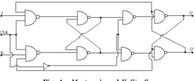
VDD is defined by the SET device parameters. Here we have implemented sequential circuits. First we have implemented a Master-slave J-K flip-flop, and using that we have implemented D flip-flip-flop, T flip-flop and 2 bit ring counter.
Fig. 4 –Master-slave J-K flip-flop
In Fig. 5, there is a J-K Master-slave flip-flop circuit. In this paper every gates are replaced using hybrid CMOS-SET. The total circuit is made of hybrid SET-CMOS NAND gate. In Fig. 5, 3 input NAND and 2 in-put NAND gates are shown.
Using these hybrid NAND gates and hybrid NOT gate (Fig. 6) we have replaced all the gates of the cir-cuit. The operations of the gates are discussed below.
4.1 Operation of a 2 i/p NAND Gate
1. When I/P1 0 and I/P2 0
Vgs of M1 will be – 0.8V (0-0.8 V) and also Vgs of M2 will be – 0.8V (0-0.8 V). Since the gate voltages are nega-tive with respect to sources, both M1 and M2 are ON. Since the gate voltages of SET1 and SET2 are equal to 0V, both SETs are OFF.
Fig. 5– 3 input NAND and 2 input NAND gate
With SET1 &n SET2 OFF, VOUT is connected to VDD via M1/M2 and the Output is high.
2. When I/P1 0 and I/P2 1
Vgs of M1 will be – 0.8V (0-0.8 V) and also Vgs of M2 will be 0 V (0.8-VDD). Therefore M1 is ON and M2 is OFF. Since the gate voltage of SET1 is equal to 0 V and SET2 is equal to 0.8 V, SET1 is OFF and SET2 is ON.
VOUT is connected to VDD via M1 and the Output is high.
3. When I/P1 1 and I/P2 0
Vgs of M1 will be 0 V and Vgs of M2 will be – 0.8V. Therefore M1 is OFF and M2 is ON. Since the gate volt-age of SET1 is equal to 0.8 V and SET2 is equal to 0 V, SET1 is ON and SET2 is OFF.
VOUT is connected to VDD via M2 and the Output is high.
4. When I/P1 1 and I/P2 1
Vgs of M1 will be 0V and Vgs of M2 will be also 0 V. Therefore, M1 is OFF and M2 is also OFF. Since the gate voltages of SET1 & SET2 are both equal to 0.8 V, both SETs are ON. With SET1 and SET2 ON, VOUT is con-nected to ground via SET1 & SET2 and the Output is low.
Thus 3 input NAND gate also operate.
4.2 Operation of the NOT Gate: [11] (Fig. 6)
SET inverter, in logic 1 or 0 regimes the output VOUT is not constant with VIN and never reaches VDD in contrast with CMOS inverter. But in our hybrid circuit, we found from the transfer characteristic that VOUT is almost con-stant with VIN in logic 1 or 0 regimes.
Fig. 6 –Circuit of hybrid SET-CMOS inverter. VIN is the
input voltage and VOUT is the output voltage
Fig. 7 –Input-output voltage transfer characteristic of the
hybrid inverter [11]
Fig. 8 –Master-slave J-K flip flop to D flip-flop
Fig. 9 –Master-slave J-K flip flop to T flip-flop
Fig. 10 –Master-slave J-K flip flop to T flip-flop
5. RESULTS AND DISCUSSION
The proposed circuits are simulated using the MIB compact model described by Analog Hardware Descrip-tion Language (AHDL) for SET and BSIM4.6.1 model for MOSFET in Tanner environment. The values of the pa-rameters used for our simulation are given in Table 2.
Table 2 – Values of Parameters used for the simulation
Device Parameters Voltage Level
SET RTD RTS 1 M , CTD CTS 0.1 aF, CG1 0.27 aF,
CG2 0.125 aF Logic 0 0 V
Logic 1 0.8 V VDD 0.8 V PMOS VTH – 220 mV,
W/L 100 nm/65 nm and default values of BSIM4.6.1 model for other parameters
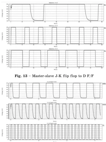
The logic operations of the circuits were first examined by simulation using T-Spice simulation software. The simulated input-output waveform is depicted in Figures. The logic operation is found to be correct. For Master-slave J-K flip-flop the simulation waveform is shown in the Figure 11. For T flip-flop the simulation result is shown in Fig. 12, the simulation waveform of D flip-flop is shown in Fig. 13 and the output of 2 bit ripple counter is shown in Fig. 14. The results obtained from the simu-lation are found to be satisfactory. The logic operations of the circuits are found to be satisfactory.
Fig. 11 –Master-slave J-K flip-flop
Fig. 12– Master-slave J-K flip flop to T F/F
5.1 Power& Delay Calculation
DESIGN AND IMPLEMENTATION OF A HYBRID SET-CMOS… J.NANO-ELECTRON.PHYS. 4, 02004 (2012)
Fig. 13– Master-slave J-K flip flop to D F/F
Fig. 14– Master-slave J-K to 2 bit ripple counter
ters given above in Table 1, the power consumption of CMOS FET is 1000nW & delay is 40 ps.
The power consumption of each 3 input NAND gate and 2 input NAND gate are 6000 nW and 4000 nW successively. So, the total power consumption of the circuit is 40000 nW. In each 3 input NAND gate 3 nos of MOSFET in the PULLUP circuit are in parallel and 3 nos MOSFET in the PULLDOWN circuit are in se-ries. So, the delay for one 3 input NAND gate is 160ps. Similarly for 2 input NAND gate, 2 nos of MOSFET in the PULLUP circuit are in parallel and 2 nos MOSFET in the PULLDOWN circuit are in series. So, the delay for one2 input NAND gate is 120 ps. In the Master-slave J-K flip flop 2 nos of 3 input NAND gates are in parallel connection, but the other 6 nos 2 input NAND gates are in 3X2 series connection. So, the total delay will be 1 time delay of 3 input NAND gate and 3 times delay of 2 input NAND gate. The total delay for Mas-ter-slave J-K flip flop will be 520 ps.
For designing in Hybrid CMOS-SET technology,
each 3 input NAND gate consists of 3 nos of CMOS Transistor in PULLUP network and 3 nos of SET in PULLDOWN network. As per the parameters given above in Table1,the power consumption of SET is 50 nW & delay is 1 ps. Power consumption of each 3 input NAND gate is 3150 nW.
Power consumption of each 2 input NAND gate is 2150 nW. So, the total power consumption of Master-slave J-K flip flop in Hybrid CMOS-SET technology is 21000 nW. Similar to the CMOS design, in each 3 input NAND gate, 3 nos MOSFET in the PULLUP circuit are in parallel connection and 3 nos of SET in the PULLDOWN circuit are in series connection. So, the delay for one 3 input NAND gate is 43 ps. Similarly for 2 input NAND gate, 2 nos MOSFET in the PULLUP circuit are in parallel connection and 2 nos SET in the PULLDOWN circuit are in series connection. So, the delay for one 2 input NAND gate is 42 ps. So the total delay for Master-slave J-K flip flop in Hybrid CMOS-SET design is 169 ps.
From the above calculation, we can show that Pow-er Consumptions & delay are quite less in Hybrid CMOS-SET technology compared to CMOS technology. In the similar way we can calculate the power con-sumption & delay for other circuits also.
6. CONCLUSION
The design and simulation of hybrid CMOS-SET sequential circuits are presented here. The output volt-age gain is estimated to be about 4.8 as determined from the slope of the transitional region. Since the SET and CMOS are placed in series, the hybridization is found to improve the gain of the inverter while the de-lay remains the same. Based on the hybrid CMOS-SET inverter, the circuits are designed and implemented. The performances of the proposed circuits are verified by simulation using T-Spice. The simulation results show that the performances of the circuits presented in this paper are satisfactory thereby establishing the feasibility of using the proposed hybrid circuits in fu-ture low power ultra-dense VLSI/ULSI circuits.
ACKNOWLEDGEMENT
Anindya Jana thankfully acknowledges the financial support obtained from State Research Fellowship, Jadavpur University, Kolkata.
S.K. Sarkar thankfully acknowledges the financial support obtained from CSIR, India vide sanction letter no. 22(0531)/101EMR-II dated 28/12/2010.
REFERENCES
1. Y. Tau, D.A. Buchanan, W. Chen, D. Frank, K. Ismail, S. Lo, G. Sai-Halasz, R. Viswanathan, H. Wann, S. Wind, H. Wong, Proc. IEEE85, 486 (1997).
2. K. Uchida, J. Koga, R. Ohba, A. Toriumi Proc. ISSCC 2, 162 (2002).
3. K. Uchida, et al., IEEE T. Electron. Dev.50, 1623 (2003). 4. C. Lageweg, S. Cotofana, S. Vassilidis, IEEE T.
Nanotech-nol.3, 237 (2004).
5. Jialin Mi; Chunhong Chen, IEEE Computer Society annual symposium on Emerging VLSI Technologies and Architectures, (2006).
6. F.Y. Chen, Y.K. Fang, C.Y. Shu, J.R. Chen, IEEE T.
Elec-tron. Dev.44, 937 (1997).
7. R.H. Chen, A.N. Korotkov, K.K. Likharev, Proc. Device
Research Conf., 44 (Charlottesville: VA: 1995).
8. Y.S. Yu, S.W. Hwang, D. Ahn, “Macromodeling of single electron transistors for efficient circuit simulation,” IEEE
T. Electron Dev.46, 1667 (1999).
9. R. Haar, R.H. Klunder, J. Hoekstra, ICECS Tech. Dig. 3, 1445.
10.Santanu Mahapatra, Adrian Mihai Ionescu, Hybrid CMOS Single-Electron-Transistor Device and Circuit De-sign (Artech House Inc.: 2006).