Copyright © 2014 IJECCE, All right reserved 109
International Journal of Electronics Communication and Computer Engineering Volume 5, Issue 1, ISSN (Online): 2249–071X, ISSN (Print): 2278–4209
Frequency Divider Digital CMOS Parallel Counter
Using Pass Transistor Logic
Amreen Parveen
Email: [email protected]
Sachin Bandewar
Email: [email protected]
Anand Kumar Singh
Email: [email protected]
Abstract – Counters are widely considered as essential building blocks for a variety of circuit operations such as programmable frequency dividers, shifters, code generators, memory select management, and various arithmetic operations. Since many applications are comprised of these fundamental operations, much research focuses on efficient counter architecture design. In this paper we design a frequency divider counter design using pass transistor logic circuit technique. The proposed counter is a 4 bit pass transistor base counter, which sequences through a fixed set of pre assigned count states, of which each next count state represents the next counter value in sequence. The counter frequency is greatly improved by reducing the gate count on all timing paths to two gates using pass transistor circuit design techniques. In our work the counter operating frequency is improved by using a parallel counter architecture of pass transistor base flipflops. This is proceeded to eliminate the carry chain delay and reduce AND gate fan-in and fan-out. The proposed counter is design for low-power and high-speed applications.
Keywords – Architecture Design, High Performance Counter Design, Parallel Counter Design.
I. I
NTRODUCTIONCounters are widely considered as essential building blocks for a variety of circuit operations such as programmable frequency dividers, shifters, code generators, memory select management, and various arithmetic operations. Since many applications are comprised of these fundamental operations, much research focuses on efficient counter architecture design. Counter architecture design methodologies explore tradeoffs between operating frequency, power consumption, area requirements, and target application specialization. Counter circuit consist of flip-flops along with combinational elements.
Depending upon the manner in which the flip-flops are triggerd, counters can be classified into two major categories:
Asynchronous counter Synchronous counter
In asynchronous counters the flip-flops is clocked by the external clock pulse and then each successive flip-flop is clocked by the Q and output of the previous flip-flop. Thus flip-flops are not clocked simultaneously. Whereas in synchronous counter, the clock input is applied to all the flip-flops simultaneously. This results an increase in the speed of operation.
There are a number of factors to consider when choosing an appropriate design for a low voltage counter. By using a high static leakage technology, a large number of transistors in the design can be a significant source of
static power dissipation. It can therefore be beneficial to keep the size of the circuit as small as possible. However, if in reducing the size of the circuit, the delay is increased, then this can negatively affect the amount of energy consumed per cycle.
II. L
AYOUTD
ESIGNC
OUNTERB
LOCKSFlip-flops are the basic building blocks of any counter circuit. In our design counter consist of a layout design of transmission gate base latch circuit connected in master slave arrangement to form the edge trigger flipflop
Fig.1. Transmission gate base D Latch
The circuit consists of a transmission gate based multiplexer and a series connected inverter. One additional inverter is used to generate the inverse of the clock input signal, required to control the transmission-gates (see fig 1). The left-to-right dataflow through the latch when CLK=1 and the feedback loop when CLK=0. When the clock input is high, the current value from the data input (D) will propagate through the transmission gate and through the two inverters. The latch is transparent, and the output value Q follows the data input value, while the Qn output generates the inverse of the data input value. When the clock signal changes to low (logical 0), the data transmission-gate is switched-off, while the feedback transmission-gate is activated and becomes conducting. As a result, the output value Q of the flipflop will be fed back into the input of the first-stage inverter. Therefore, the latch stores whatever value it hold when the clock signal changed to low.
Copyright © 2014 IJECCE, All right reserved 110
International Journal of Electronics Communication and Computer Engineering Volume 5, Issue 1, ISSN (Online): 2249–071X, ISSN (Print): 2278–4209
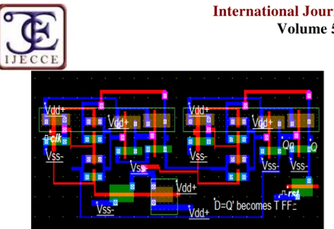
Fig.3. Layout design of Transmission gate base T flipflop
Fig.4. Simulation of Transmission gate base T flipflop Here we can use negative edge trigger flipflop. The negative edge is the edge where the clock signal Changes from 1 to 0. Thus any change in input can affect the output on at this negative edge of clock signal. Flipflops consist of two latches in series as in master slave arrangement controlled by inverted clock signals. During the high level of clock signal the master latch will turn on and slave latch will turn off. The first, called master, changes its state while Clock = 1. The second, called slave, changes its state while Clock = 0. The operation of the circuit is such that when the clock is high, the master tracks the value of the D input signal and the slave does not change. Thus the value of masters output follows any changes in D, and the value of slaves output remains constant. When the clock signal changes to 0, the master stage stops following the changes in the D input. At the same time, the slave stage responds to the value of the signal masters output and changes state accordingly. At this clock phase master latch monitors the input and during the falling edge of clock the slave latch freezes. Thus while the slave latch copies the output of the master latch. It never experiences changes during these half periods as its input, the output of the first latch is frozen. This way changes only occur at the falling edge of the control signal, when the master latch freezes and the slave latch copies its output to the flipflop’s output.
Fig.5. Four bit counter block diagram
Our design counter circuits can be built using T flip-flops because the toggle feature is naturally suited for the implementation of the counting operation. We can design this flipfop by connecting the Qn output to the D input of Master slave D flipflop shown in above figure. Fig shows four bit counter capable of counting from 0 to 15. The clock inputs of the four flip-flops are connected in cascade. The input of each flip-flop will be toggled at each negative edge of its clock. We are assuming that the purpose of this circuit is to count the number of pulses that occur on the primary input called Clock. Thus the clock input of the first flip-flop is connected to the Clock line. The other three flip-flops have their clock inputs driven by the Q output of the preceding flip-flop. Therefore, they toggle their state whenever the preceding flip-flop changes its state from Q = 1 to Q = 0, which results in a positive edge of the Q signal.
Fig 6 CMOS Layout of Four bit counter
Fig.7. Simulation of Four bit counter
III. S
IMULATIONR
ESULTS ANDP
ERFORMANCEC
OMPARISONSA. Performance Verification
Layout simulations of transmission gate base latch, flipflop, and four bit counter in microwind are conducted to compare the performances of our design. The power dissipation of master slave flipflop calculate as 9uW at 1.2V power supply at maximum delay of 0.4ns.
Copyright © 2014 IJECCE, All right reserved 111
International Journal of Electronics Communication and Computer Engineering Volume 5, Issue 1, ISSN (Online): 2249–071X, ISSN (Print): 2278–4209
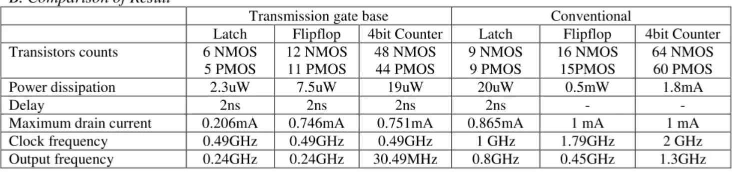
Table I
B. Comparison of Result
Transmission gate base Conventional
Latch Flipflop 4bit Counter Latch Flipflop 4bit Counter
Transistors counts 6 NMOS
5 PMOS
12 NMOS 11 PMOS
48 NMOS 44 PMOS
9 NMOS 9 PMOS
16 NMOS 15PMOS
64 NMOS 60 PMOS
Power dissipation 2.3uW 7.5uW 19uW 20uW 0.5mW 1.8mA
Delay 2ns 2ns 2ns 2ns -
-Maximum drain current 0.206mA 0.746mA 0.751mA 0.865mA 1 mA 1 mA
Clock frequency 0.49GHz 0.49GHz 0.49GHz 1 GHz 1.79GHz 2 GHz
Output frequency 0.24GHz 0.24GHz 30.49MHz 0.8GHz 0.45GHz 1.3GHz
IV. C
ONCLUSIONThe proposed counter is a 4 bit pass transistor base counter, which sequences through a fixed set of pre assigned count states, of which each next count state represents the next counter value in sequence. The counter frequency is greatly improved by reducing the gate count on all timing paths to two gates using pass transistor circuit design techniques. In our work the counter operating frequency is improved by using a parallel counter architecture of pass transistor base flipflops. All the simulation have been done on Microwind layout design tool. Simulation are perform at the voltage level of 1.2V with the load capacitance of 1fF. The input clock frequency fed in the range of 0.49GHz to 2 GHz range with the output frequency calculates in the range of 30.49MHz to 1.3GHZ. The propagation delay of the circuits is 2ns.
R
EFERENCES[1] Yin-Tsung Hwang and Jin-Fa Lin "Low Voltage and Low Power Divide-By-2/3 Counter Design Using Pass Transistor Logic Circuit Technique" IEEE Transactions On Very Large Scale Integration (Vlsi) Systems, Vol. 20, NO. 9, September 2012 pp 1738.
[2] VIJAYA Bhaskar M "Implementation Of Synchronous Up Counter By Using Self Resetting Logic" International Journal of Engineering Research and Applications (IJERA) ISSN: 2248-9622 Vol. 2, Issue 1,Jan-Feb 2012, pp.972-981
[3] R.Vennila, V.Senthil Rajan "Design Of High Performance Digital Cmos Parallel Counter" International Conference on Computing and Control Engineering (ICCCE 2012), 12 & 13 April, 2012