Copyright © 2014 IJECCE, All right reserved
Design and Implementations of Linear Congruential
Generator into FPGA
Zulfikar
Department of Electrical Engineering Syiah Kuala University, Banda Aceh 23111, Indonesia
Email: [email protected]
Hubbul Walidainy
Department of Electrical Engineering Syiah Kuala University, Banda Aceh 23111, IndonesiaEmail: [email protected]
Abstract – This paper exposes circuit design of linear congruential generator (LCG) and implementation in FPGA. The circuit is derived from LCG algorithm proposed by Lehmer. Wordlengths reduction technique has been used to simplify the circuit. Several nets connection among the blocks of the circuit are ignored or disconnected. Simulation either behavior or timing have been done successfully. Four best Xilinx chips are chosen to gather comparison data of maximum speed and area occupied. Kintex 7 is the fastest chip among all it is about 309 MHz and Spartan 6 is slowest one which is only 73 MHz. The area occupied is similar among all of the selected chips.
Keywords–Linear Congruential Generator, FPGA, Xilinx, word lengths reduction, Kintex.1
I. I
NTRODUCTIONRandom numbers have been used in daily activities since long times ago. Nowadays, a small and cheap kid’s toy containing a random number circuit inside it. For example, in a toy like (that mimic) mobile phone will ring different types of sound when the same button is pressed more than one time.
Several random numbers theory have been introduced in the last several decades. Linear congruential generator (LCG) that introduced 1954 by Lehmer [1] is the oldest and the most widely used pseudorandom number generator (PNG) [2]. Park & Miller suggest good parameters for LCG [3]. The suggestion is used in Matlab for generating uniform random numbers [4].
Many other random number generators have been proposed and also used in many applications. Blum BlumShub, Wichmann-Hill, Complementary multiply with carry, Inversivecongruential generator, ISAAC (cipher), Lagged Fibonacci generator, Linear feedback shift register, Maximal periodic reciprocals, Mersenne twister, Multiply-with-carry, Naor-Reingold Pseudorandom Function, RC4 PRGA, Well Equidistributed Long-period Linear, and Xorshift are some of the well-known methods [5]-[8].
Hardware for generating random number also available as well as its algorithm. The hardware have been used since 2008. LETech is the fastest among all hardware for computing random numbers, this hardware has been developed since 2008 [9], [10].
Research for finding the suitable algorithm of generating random number is well establish field until now. Many researchers use field programmable gate arrays (FPGA)
The authors gratefully acknowledge the financial support from Research Center of Syiah Kuala University, Indonesia under project Hibah Bersaing.
for testing their ideas. Several of these has been realized into hardware and sell into the market [5],[10].
Initially, the algorithm of LCG combined with MonteCarlo method has been used for generating non uniform random numbers using Matlab [11]. After that, we develop the circuit of random number generator and implemented in FPGA [12]. In the paper, the increment factor (c) has been ignored (c = 0). Beside, we present novel design and FPGA implementation of LCG algorithm without ignoring the increment.
The rest of this work report are organized as follows. Section II deals with theory of LCG algorithm. The design circuit of LCG for FPGA implementation and nets connections are covered in section III. Section IV provides some implementations data and analysis. Finally, the conclusions are viewed in section V.
II. L
INEARC
ONGRUENTIALG
ENERATORThere is a popular method and most used to generate random number called linear congruential generator. The idea was introduced by Lehmer according to sequential formula in (1) [1].
m c aX
Xn1( n )mod (1) Where m is modulus, a is multiplier, c is increment. Parameters a, c and m have to be chosen carefully in order to avoid repetition of similar numbers before m [6]-[8]. Park & Miller suggested a good results will be obtained by choosing c=0 [3].
The modulus m should be a large prime integer, multiplier a will be an integer in the range 2, 3, . . . , m-1. The cycle length of LCG will never exceed modulus m, but it can be maximized using three following conditions [7], [13]:
c is relatively prime to modulus m,
multiplier a-1 is a multiple of every dividing modulus m,
multiplier a-1 is a multiple of four when modulus m is a
multiple of four.
III. LCG C
IRCUITD
ESIGNA. General Circuit of LCG
Inter
The block diagram of Fig. 1 is inv operation such as multiplication, additio comparison. In order simplify the proc designed using word lengths reduction te been suggested in [14]. Then subtarcto blocks can be removed, as shown in the F
The designed circuit consist of a multiplier, an adder, a buffer (required buffers (required enable). Ports input S used to pass initial value, multiplier and circuit. Meanwhile, port O is used to resulted random numbers.
Fig.2. Ge The circuit is controlled by two signals Initially, signal reset have to be HIGH clear the previous stored values in the
enable determine when the operation s
Pre-defined value (seed), increment and be available at the input ports before e (reset=LOW). Then, every times cloc random number resulted. Fig.3shows the signal controls.
Fig.3. Signal controls of the designed
B. Wordlengths Reduction
The circuit of Fig. 2 can be used for The reduction of word lengths have to c to avoid undesirable operation result. LCG is designed for using maximum w bit, the nets configurations of multiplier block are shown in the Figs. 4 and 5.
ternational Journal of Electronics Communication an Volume 5, Issue 4, ISSN (Online): 2249–071X,
involving arithmetic ition, subtraction and rocess, the circuit is n technique that has ctor and comparator
e Fig. 2.
a multiplexer, a ed clear), and three t Seed, A and C are d increment into the to taking out the
Fig.1. Block diagram o
2. General circuit of linear congruential generator als enable and reset.
GH (enable=LOW) to the buffer B4. Signal n should be started. nd multiplier have to
enable goes HIGH
lock goes HIGH, a the circuit of the two
ned LCG circuit
or any word lengths. to construct carefully lt. For example, the word lengths of 8 lier block and adder
Fig.4.Word lengths reductio
Fig.5.Word lengths reduc Based on arithmetic rules an multiplication of B4(8 bit) and bit at the output. In the des (disconnected) the seven-highe this design is shown in the Fig. same thing to the nets of adder (M(8)) disconnected as shown in
and Computer Engineering 1X, ISSN (Print): 2278–4209
m of LCG operation
ction in multiplier’s block
uction in adder’s block
Co
IV. I
MPLEMENTATIONS ANDD
A. Behavior Simulation
The circuit in the Fig. 2 has been FPGA program. The simulations have Xilinx ISE design suite. Some important result is shown. The comparison of are beendone over several Xilinx’s chips.
Fig.6. Simu
Fig.7. Simu
Fig.8. Simu
B. Synthesis result
Some important synthesis data of the using modulus m=255 into Xilinx Virtex HDL Synthesis Report
Macro Statistics
# Multipliers : 1
8x8-bit multiplier : 1
# Adders/Subtractors : 1
16-bit adder : 1
# Registers : 4
8-bit register : 4
# Multiplexers : 1
8-bit 2-to-1 multiplexer : 1 ---Slice Logic Utilization:
Number of Slice Registers: 16 out of Number of Slice LUTs: 10 out of Number used as Logic: 10 out of Slice Logic Distribution:
Copyright © 2014 IJECCE, All right reserved
D
ISCUSSIONSn implemented into ve been done using tant data of synthesis area and speed have
Fig.6 shows behavior simu m=255, seed=7, multiplier a=3 be seen the resulting numbers a and all numbers are smaller than Figs.7 and 8 show behavior si m=216–1 and m=231–1 respec produced there never exceed mo
imulation behavior result of m=255, seed=7, a=3, c=1
mulation behavior result of m=216-1, seed=7, a=3, c=1
mulation behavior result of m=231-1, seed=7, a=3, c=1
the designed circuit tex 7 chip are:
---of 437600 0%
of 218800 0% of 218800 0%
Number of LUT Flip Flop pairs Number with an unused Flip Flo Number with an unused LUT: Number of fully used LUT-FF p Number of unique control sets: ---Minimum period: 3.710ns 269.513MHz)
Minimum input arrival time befo Maximum output required time Maximum combinational path d From HDL synthesis report, an 8x8-bit multiplier, 16-bit ad 8-bit 2-to-1 multiplexer. In term the design occupies 16 slice re The distribution of slice logic fr 9 for fully used LUT-FF pairs, unused flip-flop. The circuit als sets.
mulation result of modulus =3 and increment c=1. It can s are random starting from 7 han 255.
r simulation result of modulus pectively. Also all number
modulus.
irs used: 17
Flop: 1 out of 17 5% : 7 out of 17 41% F pairs: 9 out of 17 52%
s: 2
---s (Maximum Frequency: efore clock: 2.023ns
e after clock: 0.575ns th delay: No path found
Inter
The speed of the circuit limited to when it is implemented into Virtex 7 arrival time before clock is 2.023 ns. Th should be available at input port befo maximum output required time after cloc
F
D. Comparison
Four best Xilinx chips has been ch compare the speed and area of the design shows comparison of maximum freque
modulus m=255 (8 bit), m=216-1 (16 bit) bit) over Virtex 7, Spartan 6, Kintex 7 an
Table I : Maximum frequency comparis chips
Chips Maximum Freque
8 bit 16 bit
Virtex 7 270 270
Spartan 6 154 154
Kintex 7 309 270
Zynq 272 272
For m=255, the fastest chip is Kintex one is Spartan 6, but for m=216–1, th Zynq. In general, Kintex 7 is the fastest the slowest chip. A more clear view of seen graphichally in the Fig. 10.
Fig.10. Comparison of maximum frequen chips
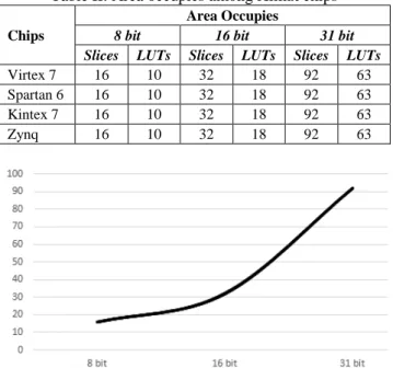
Table II views area comparison am chips. It can be seen that all chip occup For m=255, the chips required 16 slices a
ternational Journal of Electronics Communication an Volume 5, Issue 4, ISSN (Online): 2249–071X,
to around 270 MHz 7. Minimum input This means the data fore that time. The lock is 0.5775 ns.
C. Timing Simulation
Fig.9 shows a close look of There are some glitches when th to 202. This is because time varied. This variation range fr (post-PAR static timing report).
Fig.9. A close view of timing simulation
chosen in order to igned circuit. Table I quency required for bit) and m=231-1 (31 and Zynq chips.
rison among Xilinx
uency (MHz)
it 31 bit
139 73 158 140 tex 7 and the slowest
the fastest chips is test and Spartan 6 is of this figure can be
uency among Xilinx
among four Xilinx upies the same area. es and 10 LUTs. The
area becomes twice when using Meanwhile when the modulus occupied slices and LUTs incr Figs. 11 and 12 show a more cle
Table II: Area occupies a
Chips
Are 8 bit
Slices LUTs Slic
Virtex 7 16 10 32
Spartan 6 16 10 32
Kintex 7 16 10 32
Zynq 16 10 32
Fig.11. Comparison of slice utiliz
Fig.12. Comparison o
and Computer Engineering 1X, ISSN (Print): 2278–4209
of timing simulation result. n the number change from 67 e from clock edge to pads from 9.399 ns to 9.818 ns rt).
sing modulus around 16 bits.
lus is changed to 31 bits, the
crease to around three time. clear views of this behavior. ies among Xilinx chips
rea Occupies
16 bit 31 bit
Slices LUTs Slices LUTs
32 18 92 63
32 18 92 63
32 18 92 63
32 18 92 63
tilization among Xilinx chips
Copyright © 2014 IJECCE, All right reserved
V. C
ONCLUSIONDesign and implementation of linear congruential generator into FPGA have been done successfully. It is required special care of wordlengths connecting among the blocks of the circuit. By applying wordlengths reduction technique, a more efficient circuit has been obtained.
The maximum frequency of the design circuit is 309 MHz (Kintex 7, m=255), and the minimum frequency is 73 MHz (Spartan 6, m=231–1). Kintex 7 is the best chip of applying the design LCG circuit.
Further improvement of the design may be obtained by analyzing behavior of seed, multipliera and increment c. Finally, it is difficult to compare the result to the previous works since there is no available similar circuit or method before.
R
EFERENCES[1] D. H. Lehmer,“Random number generation on the BRL high speed computing machines,”by M. L. Juncosa. Math. Rev. 15 (1954), 559
[2] http://en.wikipedia.org (2014) - Linear congruential generator, 10th March http://en.wikipedia.org/wiki/ Linear_congruential _generator
[3] S. K. Park, and K. W. Miller, “Random number generators: good
ones are hard to finnd,”Association for Computing Machinery,
31(10), pp: 1192-2001, 1988.
[4] Numerical Computing with MATLAB, By Cleve B. Moler,
SIAM,2008
[5] http://en.wikipedia.org (2014) - List of random number generators, 11th March http://en.wikipedia.org/wiki/List_of_ random_number_generators
[6] N. Harald,“Random Number Generation and Quasi-Monte Carlo
Methods,” Society for lndustrial and Applied Mathematics,
Philadelphia, 1992.
[7] A note on random number generation, Christophe Dutang and Diethelm Wuertz, September 2009
[8] Wolfram Mathematica ® Tutorial Collection, RANDOM NUMBER GENERATION, 2008
[9] http://www.letech.jpn.com (2014) - Genuine Random Number Generator (GRANG), 10th March http://www.letech.jpn.com/ rng/about_rng_e.html
[10] http://en.wikipedia.org (2014) - Comparison of hardware random number generators, 10th March http://en.wikipedia.org/wiki/ Comparison_of_hardware_random_number_generators
[11] Zulfikar, “Generating Non Uniform Random Numbers Using
Residue and Rejection Methods,” Transaction of Journal
Rekayasa Elektrika, Vol. 8 No. 2, October 2009
[12] Zulfikar, “FPGA Implementations of Uniform Random Number
based on Residue Method,” Transaction of Journal Rekayasa
Elektrika, Vol. 11 No. 1, April 2014
[13] D. E. Knuth, “The Art of Computer Programming: seminumerical algorithms,” Vol. 2,3rd edition edn,
Massachusetts: Addison-Wesley, 2002
[14] Zulfikar, “Novel Area Optimization in FPGA Implementation
Using Efficient VHDL Code,”Transaction of Journal Rekayasa
Elektrika, Vol. 10 No. 2, October 2012
[15] Zulfikar, Abbasi, S A and Alamoud A R M, “FPGA Based
Complete Set of Walsh and Inverse Walsh Transforms for Signal
Processing,” Transaction of Electronics and Electrical
Engineering Journal, Vol.18. No. 8, Pp: 3-8, October 2012.
A
UTHOR’
SP
ROFILEZulfikar
was born in Beureunuen, Aceh, Indonesia, in 1975. He received his B.Sc. degree inElectrical Engineering from North Sumatera University, Medan, Indonesia, the M. Sc. Degree inElectrical Engineering from King Saud University, Riyadh, Saudi Arabia, in 1999 and 2011,respectively.
He joined as teaching staff in the Department of Electronics at Politeknik Caltex Riau, Pekanbaru, Indonesia in 2003. He served as head of Industrial Control Laboratory, Politeknik Caltex Riau from 2003 to 2006. In 2006, he joined the Electrical Engineering Department, Syiah Kuala University.His current position is head of Digital Laboratory, and his current research interests include VLSI design and System on Chips (SoC).
Hubbul Walidainy
was born in Banda Aceh, Aceh, Indonesia, in 1973. He graduated from Electrical Engineering Department at Gadjah Mada University, Yogyakarta, Indonesia, in 1998. The Master Degree inElectrical Engineering from Gadjah Mada University, Yogyakarta, Indonesia, in 2003.