Implementation of Multi-Protocol, Data Acquisition
With High Speed USB Interface,
Using FPGA
S. Thanee S. Somkuarnpanit S. Khuntaweetep
Abstract
—This paper describes the implementation of the FPGA as a data acquisition system with high- speed USB interface. This can simplify the data interfacing to the PC by installing most data transfer protocols into one system. The FPGA has the advantage that it allows individual modules on a chip to work independently from each other. Therefore, we can utilize the FPGA as a performance solution for a system which is multi-channeled, with connections to four ADC signals, with the four different protocols of: Parallel, SPI, I2C and One-Wire. In addition, the visual C++ programming for the user interface and data storage application, on a PC, helps this design to respond better to high rates of data acquisition.Keywords: Data acquisition, FPGA, high-speed USB
I. Introduction
The data acquisition system has been broadly applied in the automatic test and measurement systems for engineering and science, as we are able to either adjust or define values via controlling software [1]. The main function of the software is to collect the data from any peripheral, input devices, such as meters or sensors and to transfer it into the main database and show the results, in real time, on the screen, or to display them in a summary graph.
This paper proposed the design of the data acquisition system using FPGA [3] interfaced to a PC [2]. The system has the capability of receiving digital signals from multi-channel sensors with four, different, ADC protocols.
II. Overall System
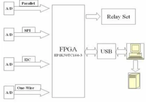
The overall system is shown in Figure 1. Itrepresents connections to four different ADC (analog to digital converter) sensors with four different protocols: Parallel,
SPI, I2C andOne-Wire. The FPGA would collect individual data from all ADC sensors.
The system would process, separately, in individual protocols, and consequently produce a stream of data through the output USB port [4], which sends the ADC data to the PC.
Manuscript received December 7, 2009.
S. Thanee is a graduate student, with a Master’s Degree, in the Faculty of Engineering at King Mongkut’s Institute of Technology, Ladkrabang, Bangkok Thailand (e-mail: [email protected]).
S. Somkuarnpanit is now with the Department of Electronics, Faculty of Engineering at King Mongkut’s Institute of Technology, Ladkrabang, Bangkok Thailand (e-mail: [email protected]).
S. Khuntaweetep is with the Department of Electronics, Faculty of Engineering at King Mongkut’s Institute of Technology, Ladkrabang, Bangkok Thailand (e-mail: [email protected]).
There would be a specific application program to prepare the PC to wait for the data from a USB port. It would then interpret the data into separate data bytes for individual channels. Consequently, the data can be shown to the user, and saved to the main database at the same time. Alternatively, the user could control the system by sending instructions via the USB port.
Figure 1 The overall system diagram.
III. Processing Unit
The processing unit employed for this design is EP1K10TC144-3 from the Altera Company. It has a capacity of 2,880 logic elements, or about 50,000 gates, consisting of 40,960 internal ram bits and 102 input/output ports for connection to external hardware. It supports 3 level power supply of 5V, 3.3V and 2.5V. The maximum working frequency is 180 MHz. This design has used VHDL as the language [7][8] for program writing code.
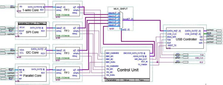
The chip is the central point of acquisition for the all sensors. Its responsibility is to bridge between the ADC inputs and the USB connection i.e. sending/receiving data to, and from, the PC. Figure 2 illustrates the internal modules within the FPGAchip [6]. These modules are described as below:
Parallel Protocol: This protocol is the traditional type for most ADCs. It has the advantage of high speed data throughput. This design uses ADC0820 as a template example. Figure 3 represents a simulation for acquiring data from this ADC. There are two main steps in the conversion process:
• FPGA sends a ‘start’ signal to activate the ADC and then waits for an ‘acknowledgement’ signal.
• After the ADC finishes converting the data, it will send an acknowledgement signal to the FPGA, then the FPGA will read all the data from the bus. After that it will send another ‘start’ signal to activate the ADC again for data acquisition on the next read cycle. Proceedings of the International MultiConference of Engineers and Computer Scientists 2010 Vol I,
IMECS 2010, March 17 - 19, 2010, Hong Kong
ISBN: 978-988-17012-8-2
ISSN: 2078-0958 (Print); ISSN: 2078-0966 (Online)
It can be seen that, this data acquisition is very simple and fast. Thus, this protocol should properly work within a high speed system.
Figure 3 Simulated parallel communication protocol.
Serial Peripheral Interface (SPI) Protocol: This protocol was developed by Motorola to accomplish easy communication, and to reduce I/O ports. This design utilizes MCP3201 for building connections to FPGA. Figure 4 shows a simulation of how the FPGA obtains data from an ADC. The steps of this ADC data acquisition look like the previous protocol. The FPGA would send the control signal to activate ADC and the ADC would send the acknowledgement signal back, after it finishes converting data, to tell the FPGA to read the data from its output. The difference from the previous protocol is that the FPGA would read the stream of data in a serial pattern instead, from MSB to LSB.
Figure 4 Simulated SPI communication protocol.
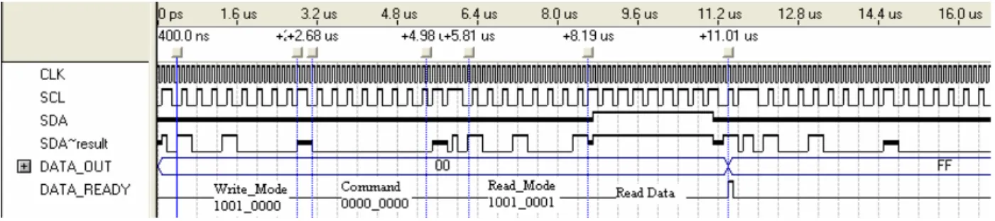
Inter-Integrated Circuit Protocol (I2C): I2C communication is a protocol which is designed to reduce the I/O ports. It requires only two signal connection wires called SCL and SDA. This design uses PCF8591 ADC as a template example. The procedure for this ADC data acquisition is quite complicated, as in the following steps:
• The FPGA sends a signal to start the bus and to identify the address of the device.
• The FPGA defines the write mode and sends a command to the ADC it wants to convert.
• The FPGA defines the ‘read’ mode and identifies which channel it wants to read from.
• The FPGA reads the data from the I2C bus.
At this point, the data reading has completed 1 time cycle. Figure 5 illustrates the example of data reading by this protocol. We can see that one reading cycle of this protocol takes more time than the previous protocols whereas it has the good point of using only two wires in the data communication.
One-Wire Protocol: This protocol employs only one signal line in communications. The bus is not active unless all data has been transferred. We used the temperature sensor DS1820 as the input of this One-Wire acquisition data protocol.
The protocol separates the data bit by a time slot. It has a length of between 60-960 µs, depending on the user definition and the status of communications between master and slave devices. There are four status types:
• Reset: used to start the communication.
• Write data “1” to slave device.
• Write data “0” to slave device.
• Read data from slave.
The first step for this protocol is the ‘reset’ from the FPGA (master device). The FPGA would send a reset signal to the bus, and wait for an acknowledgement signal from sensor (slave device). After receiving the acknowledgement signal, the FPGA would send the address command to identify the sensor and let it start data conversion.
The FPGA would wait for a sensor processing the command. Then it would send the reset signal and identify the device address again, followed by the ‘read’ command to the sensor, to read data from the sensor memory one by one from LSB to MSB. Finally, it would send the reset signal again to the bus and wait for an acknowledgement signal.
Proceedings of the International MultiConference of Engineers and Computer Scientists 2010 Vol I, IMECS 2010, March 17 - 19, 2010, Hong Kong
ISBN: 978-988-17012-8-2
ISSN: 2078-0958 (Print); ISSN: 2078-0966 (Online)
Figure 6 Simulated Control Unit and USB Controller communication
After these procedures, the data read procedure has completed one time cycle. To obtain more data, the FPGA would process the same steps again. Figure 7 displays the simulated communications for ‘reset’, ‘acknowledgement’, and ‘write’ “1100 1100” data.
Figure 7 The One-wire communications protocol.
Control Unit and USB Controller: If there is any data appearing on the FIFO buffer, the control unit would determine which channel the data is from. Subsequently, it would send a one-byte data code to the USB port. This first data byte informs the application program on the PC which channel the following data is from. Then it will send a signal to the USB controller again to send the data, in the FIFO, to the USB port byte by byte, until the FIFO is empty. This will mean the end of the data sending procedure in that individual channel. If there is data waiting to be sent out from another FIFO channel, the FPGA will repeat the same procedures. Figure 6 shows a simulation for interconnection between the control unit and the USB controller.
IV. The PC Interfacing
The PC interfacing used in this design is the high-speed USB which can transfer data at the rate of 480 Mbps. The transfer operation is achieved via ‘frames’, with a period of 125 µs. Each frame consists of a number of ‘Transactions’, each which consists of a number of Packets. These packets include information about the type of transaction, the address of the USB device, and the number of the end points required, in addition to data, and CRC packets, and a synchronization packet.
The FT2232H chip from FTDI Corp. [5] has been used to implement this protocol in the design. It is a dual USB to parallel FIFO, bi-directional, data transfer chip with 4 kilobytes FIFO Tx and Rx buffers, which handles the entire USB protocol on the silicon level. The manufacturer provides the D2XX.DLL driver, which allows full accessibility to all the chip features through a DLL function. Figure 5 Simulated I2C communication protocol
Figure 8 FT2232H/FPGA interfacing Proceedings of the International MultiConference of Engineers and Computer Scientists 2010 Vol I,
IMECS 2010, March 17 - 19, 2010, Hong Kong
ISBN: 978-988-17012-8-2
ISSN: 2078-0958 (Print); ISSN: 2078-0966 (Online)
Figure 9 The sample displays in the application program
This chip provides an interface between the FPGA and the USB port with an 8 bit, bi-directional data bus, plus five control signals and one clock signal.Figure 8 illustrates the FT2232H/FPGA interfacing.
V. The Application
The application program of this design was written in the visual C++ language [9] in the following 3 layer structure : Presentation layer: for plotting all the data graphs to be monitored by the user.
Hardware layer: continuously issuing ‘read/request’ in a "reading worker thread" that will return one or more data items and put the data in a queue which the data acquisition layer can read from.
Data acquisition layer: When the data requires some kind of interpretation, each sensor will have a thread that collects the data, and saves it in the PC. When this thread runs, it moves the data from the queue, shared with the hardware layer, into its own container, and updates the current value shared with the presentation layer.
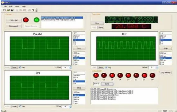
This application is responsible for reading data from each protocol and presenting it to the user in a graphic oscilloscope-like form. Since the one-wire protocol is used for temperature sensors, it will show the temperature level number instead. Figure 9 displays an example of the application program in operation.
VI. Conclusions
From our simulation results, we can see that the parallel protocol is the fastest, whereas, it uses the most connective wires. On the other hand, the I2C or one-wire protocol requires only two wires and one wire, respectively, for the connection, but the bit transfer rate is much slower than general the ADC. We can use this knowledge when considering the use of a protocol in most applications.
Finally, we may now claim that our data acquisition system with channels for multiple protocols is a useful solution. Consisting of input channels with individual ADC
protocols, our system allows the channels to work independently from each other. In addition, with a large number of I/O ports in the FPGA, it is feasible to add more channels in the future. Eventually, we may be able to utilize the maximum of 102 I/O ports, being the maximum number, for this FPGA.
References
[1] Ziad Salem, Ismail Al Kamal, Alaa Al Bashar “A Novel Design of an Industrial Data Acquisition System”, Proceeding of International Conference on Information and Communication Technologies: From Theory to Applications, ICTTA 2006. pp. 2589-2594.
[2] Jorge Yáñez, David Quintana, Camilo Quintáns, José Fariña,
Juan J. Rodríguez-Andina,” FPGA-based system for the
education in data acquisition and signal generation”, Proceeding of Industrial Electronics Society Conference, IECON 2005. pp. 2168-2173.
[3] A. Sagahyroon ,T. Al-khudairi, ”FPGA Based Acquisition of Sensor Data” Proceeding of International Conference on Industrial Technology, ICIT 2004. pp. 1398 – 1401.
[4] M. Popa, M. Marcu, A. S. Popa,” A Microcontroller Based Data
Acquisition System with USB Interface”, Proceeding of
International Conference on Electrical, Electronic and Computer Engineering, ICEEC 2004 pp. 206-209
[5] FTDI Corporation., www.ftdichip.com, Glasgow City,
Scotland,
[6] Hamblen J., Furman M., “Rapid Prototyping of Digital
Systems”, Quartus II Edition, Springer Science+Business Media Inc., New York, USA, 2006
[7] Dluglas L. Perry “VHDL Programming By Example”, Forth Edition, McGraw-Hill Company, USA, 2002.
[8] Pong P. Chu “RTL Hardware Design Using VHDL”, First Edition, John Wiley & Sons, Inc., Hoboken, Canada, 2006.
[9] George Shepherd, David Kruglinski“Programming with
Microsoft Visual C++ .NET”, Sixth Edition, Microsoft Press, Washington, USA, 2003.
Proceedings of the International MultiConference of Engineers and Computer Scientists 2010 Vol I, IMECS 2010, March 17 - 19, 2010, Hong Kong
ISBN: 978-988-17012-8-2
ISSN: 2078-0958 (Print); ISSN: 2078-0966 (Online)