PONTIFÍCIA UNIVERSIDADE CATÓLICA DO RIO GRANDE DO SUL FACULDADE DE INFORMÁTICA
PROGRAMA DE PÓS-GRADUAÇÃO EM CIÊNCIA DA COMPUTAÇÃO
DISTRIBUTED
MEMORY
ORGANIZATION
WITH
SUPPORT
FOR
DATA
MIGRATION
FOR
NOC-BASED
MPSOCS
TALES MARCHESAN CHAVES
Submitted in partial fulfillment of the requirements for the degree of Master of Science in Computer Science at Pontifícia Universidade Católica do Rio Grande do Sul.
Advisor: PhD. Fernando Gehm Moraes
Dados Internacionais de Catalogação na Publicação (CIP)
C512d Chaves, Thales Marchesan
Distributed memory organization with support for data migration for NOC-based MPSOCS / Thales Marchesan Chaves. – Porto Alegre, 2011.
90 f.
Diss. (Mestrado) – Fac. de Informática, PUCRS.
Orientador: Prof. PhD. Fernando Gehm Moraes.
1. Informática. 2. Multiprocessadores. 3. Migração de Dados
(Informática). 4. Memória de Computador. I. Moraes, Fernando
Gehm. II. Título.
CDD 004.35
Ficha Catalográfica elaborada pelo
AGRADECIMENTOS
Logo de início, o mestrado parece fácil. Muitos colegas, coisas novas, tudo divertido. Até que ele começa mostrar sua verdadeira face, torna-se difícil e cansativo. Perdemos alguns colegas que abandonam a batalha. Mas guerreiro que é guerreiro persiste, confia em deus, e acaba a sua jornada com sucesso.
A minha jornada foi de grande aprendizado, alegrias, tristezas, cansaços, esforços, mas no fim, valeu muito a pena. Eu faria novamente. Desta forma, gostaria de agradecer a todos que me ajudaram e apoiaram durante estes dois anos (2010-2012). A meus pais, Carlos e Joseane, muito obrigado pelo incentivo, apoio e educação que me deram. A minha companheira, Bruna, obrigado pela enorme paciência, amor e compreensão que teve e ainda tem comigo. Gostaria também de agradecer a meus avós paternos, Ocir e Rodi, que sempre me apoiam, em qualquer momento da minha vida. Também aos meus tios Toni e Lea, que durante a minha infância e adolescência foram como meus segundos pais. Gostaria também de agradecer ao meu primo Rafael, que sempre me ajudou, principalmente desde que me mudei para Porto Alegre. Ao restante da família, meus sinceros agradecimentos pelo pensamento positivo e os momentos de descontração.
Gostaria de agradecer enormemente aos professores do PPGCC, principalmente, ao meu orientador, Fernando Moraes, por me aceitar como aluno do mestrado, me dar a oportunidade de conhecer um mundo novo composto por NoCs e MPSoCs. Gostaria de agradecer também aos professores que me acompanharam e avaliaram durante as várias bancas do mestrado, dentre estes: Prof. Ney Calazans, Prof. Gustavo Fernandes, Prof. Cézar Marcon e o Prof. José Luiz Güntzel.
Gostaria de agradecer aos colegas mestrado, companheiros de noitadas na PUC, fazendo trabalhos. Alguns destes são membros do grupo GAPH, outros não: Eduardo Antunes, Everton Carara, Thiago Raupp, Carlos Petry, Eduardo Wachter, Marcelo Mandelli, Julian Pontes, Rafael Soares, Matheus Moreira e a todos os demais.
ORGANIZAÇÃO DE MEMÓRIA DISTRIBUÍDA COM SUPORTE À
MIGRAÇAO DE DADOS PARA MPSOCS BASEADOS EM NOCS
RESUMO
O avanço da tecnologia de semicondutores possibilitou o desenvolvimento de sistemas intra-chip (SoCs) que integram, em um mesmo chip, diversos elementos de processamento (PEs) e módulos de memória. SoCs que possuem mais de um PE são denominados de sistemas intra-chip multiprocesados (MPSoCs).
À medida que o número de PEs aumenta em um MPSoC, torna-se necessário o uso de técnicas que resultem em um baixo consumo de energia, baixa latência na comunicação e escalabilidade. Em MPSoCs baseados em redes intra-chip, com blocos de memória compartilhada (cache L2), o aumento no número de PEs culmina no aumento da quantidade de acessos realizados a estes módulos. Isto torna a organização de memória um dos componentes mais críticos destes sistemas, tendo em vista que a mesma pode apresentar um alto consumo de energia e alta latência de resposta. Fatores como estes podem limitar o uso e a escalabilidade destes sistemas.
Dentre os fatores que afetam o consumo de energia e a latência da organização de memória de um MPSoC estão: o protocolo de coerência de cache e o mapeamento dos dados de aplicações. Este trabalho propõe a utilização de uma organização de memória cache L1 que possui latência de acesso não uniforme, onde acessos realizados podem ser destinados a diferentes bancos de memória cache L2 (NUCA – non uniform cache access architecture). Além disso, o presente trabalho explora os serviços físicos providos pela rede intra-chip, tais como multicast e prioridades, para otimizar a implementação de um protocolo de coerência de cache baseado em diretório. Os resultados obtidos mostram uma redução média de 39% no consumo de energia de comunicação e 17% de latência em transações do protocolo de coerência quando explorando serviços físicos oferecidos pela rede intra-chip.
Além disso, a fim de melhorar o posicionamento de dados de aplicações, é proposto um protocolo de migração de dados que posiciona os dados utilizados por uma região de PEs em um banco de memória cache L2 próximo. Com a utilização deste protocolo, é possível obter uma redução média de 29% no consumo de energia nos acessos à memória cache L2.
Palavras Chave: MPSoCs baseados em NoC, Sub-sistema de Memória, Coerência de
DISTRIBUTED MEMORY ORGANIZATION WITH SUPPORT FOR
DATA MIGRATION FOR NOC-BASED MPSOCS
ABSTRACT
The evolution in the deployment of semiconductor technology has enabled the development of System-on-Chip (SoCs) that integrate several processing elements (PEs) and memory modules in a single chip. SoCs that integrate several PEs are referred as Multiprocessor System-on-Chip (MPSoCs).
As the number of PEs increases in an MPSoC, techniques that present low energy consumption, low latency and scalability become necessary. In NoC-based MPsoCs that adopt the Shared Memory model in the L2 cache, as the number of PEs increases, the number of accesses to memory modules also increases. This makes memory organization one of the most critical components of the system because it can present high energy consumption and high latency. Such factors may limit the use and scalability of MPSoC systems.
Among the factors that contribute to increase latency and energy consumption in memory organizations are: the cache coherence protocol and the mapping of application's data. This work proposes the use of a cache memory organization that presents non-uniform access latency, where accesses to the L1 cache can target different L2 cache banks (NUCA – non uniform cache access architecture), as a function of the address being accessed. Additionally, this work proposes the exploration of the physical services provided by the network-on-chip, such as multicast and priorities, to optimize the implementation of a directory-based cache coherence protocol. The obtained results show an average reduction of 39% in communication energy consumption and 17% reduction in latency for transactions of the cache coherence protocol when exploring NoC services.
To improve placement of application's data, a data migration protocol is proposed. The goal of the protocol is to approximate L2 cache blocks to PEs that are mostly accessing it, moving blocks to a closer L2 cache bank, if available. By using a data migration protocol, an average reduction of 29% was obtained in the energy consumption of cache accesses.
LIST OF FIGURES
Figure 1 – DCOS switch architecture proposed by [KIM06]. ... 22
Figure 2 – Distributed Shared Memory architecture proposed by [YUA08]... 23
Figure 3 – NoC view of TSP partitions and positioning of MMU and PE nodes. ... 24
Figure 4 – Multiprocessor architecture proposed by [MON06]. ... 25
Figure 5 – In the left, it is shown the architecture of the HEAD node. In the right, each circle comprises a cluster region [YUA08]. ... 28
Figure 6 – PE architecture with L2 cache and VTC modules [JER05]. ... 29
Figure 7 – NoC-based MPSoC architecture with an exclusive bus for cache coherence transactions [CHT09]. ... 30
Figure 8 – Cluster architecture proposed by Nafziger et al. [NAF10]. ... 33
Figure 9 – Router architecture proposed by Eisley et. al [EIS08] to guide evicted blocks to unused cache blocks. ... 34
Figure 10 – HeMPS-Q platform architecture. ... 36
Figure 11 - Example of label assignment based on a Hamiltonian path in a 4x4 mesh. .... 37
Figure 12 – Two examples of multicast messages. The first shows an example of a multicast message to network addresses 8, 10, 12 and 14. The second shows a multicast message that target network addresses 5, 3 and 1. ... 38
Figure 13 - HeMPS Microkernel Layers. ... 40
Figure 14 - TCB structure described in C language. ... 42
Figure 15 - Intertask communication between tasks located at different processors. ... 43
Figure 16 - HeMPS Generator Framework. ... 45
Figure 17 - MPSoC with a two level memory hierarchy – shared memory and caches (only Slave-PEs may contain caches). ... 47
Figure 18 - Internal modules of the PLASMA processor. ... 49
Figure 19 – Internal architecture of the L2 cache module. ... 49
Figure 20 - Packet format for shared memory operations. ... 51
Figure 21 – Structure of an entry of the directory memory. ... 52
Figure 22 – Example of address space division in cache banks, assuming four blocks per L2 cache bank. ... 53
Figure 23 – Sequence diagram of all possible actions performed by the microkernel in a read operation. ... 55
Figure 24 - Sequence diagram for a request of exclusivity on a shared cache block. ... 59
Figure 25 - Sequence diagram for a read operation of a modified cache block. ... 59
Figure 26 - Sequence diagram for a write-back operation after a write request. ... 60
Figure 27 - MPSoC configuration: 3x2 NoC, 5 PEs (1 master, 4 slaves) and 1 L2 cache.. 61
Figure 28 - Sequence diagram for the T state. ... 61
Figure 29 – Regions (rectangles in the figure) defined according to the minimum distance to the L2 cache bank... 64
Figure 30 – Block access accounting algorithm. ... 65
Figure 31 – Circular mechanism for verifying free blocks in the L2 cache bank. ... 66
Figure 32 – Four steps of the data migration process. ... 67
Figure 34 – Free block slot request format. ... 67
Figure 35 – Free block slot response format. ... 68
Figure 36 – Block migration message format. ... 68
Figure 37 – Update address mapping table message format. ... 68
Figure 38 – Cache miss average latency (AL), expressed in number of clock cycles, for a varying number of applications tasks and L2 cache banks for the mostly-read set. ... 71
Figure 39 - Average write latency (AL), shown in number of clock cycles, for a given number of L2 cache banks. Also, worst write request latency (WL) for a given configuration of cache banks. ... 72
Figure 40 – Core part of the implementation of the matrix multiplication for the HeMPS platform. ... 73
Figure 41 – Two different implementations of a MM application using 2 tasks. ... 73
Figure 42 – Two different implementation of a MM application using 3 tasks. ... 74
Figure 43 – Tasks graphs for equation solver application. ... 75
Figure 44 - Example of an application reading and writing to the shared memory. ... 77
Figure 45 - Energy consumption of the read operation on a modified block as the number of hops increases. ... 78
Figure 46 - Number of cycles required to execute a read operation on a modified block varying the location of the modified block. ... 79
Figure 47 - Energy consumed to execute a read operation on a modified block varying the location of the modified block. ... 79
Figure 48 –Task mappings for the T state optimization. ... 80
Figure 49 – Example scenario 1 for data migration, evaluates migration of a block from a distant region. ... 81
Figure 50 – Example scenario 2 for data migration, evaluates migration of a block to a neighbor region. ... 82
Figure 51 – Matrix multiplication task mapping. ... 82
LIST OF TABLES
LIST OF ACRONYMS
2D Two dimensional
ACK Acknowledgment
API Application Programming Interface CMP Chip Multi Processor
CPU Central Processing Unit CSM Centralized Shared Memory DCOS Directory Cache On Switch DDR Double Data Rate
DM Distributed Memory
DMA Direct Memory Access
DRAM Dynamic random access memory DSM Distributed Shared Memory DSP Digital Signal Processor
DVFS Dynamic Voltage Frequency Scaling
FBS Free Block Searcher
FFT Fast Fourier Transform FSM Finite State Machine GPS Global Positioning System
I/O Input/Output
IC Integrated Circuit IP Intellectual Property
ISA Instruction Set Architecture ISS Instruction Set Simulator
KPN Kahn Process Network
MMU Memory Management Unit
MOESI Modified Owned Exclusive Shared Invalid MPI Message Passing Interface
MPSoC Multiprocessor System on Chip MSI Modified Shared Invalid Protocol
NI Network Interface
NoC Network on Chip
NUCA Non Uniform Cache Access
PC Program Counter
PCB Printed Circuit Board
PE Processing Element
POSIX Portable Operating System Interface QoS Quality Of Service
RAM Random Access Memory
RISC Reduced Instruction Set Computer RTL Register Transfer Level
RTOS Real Time Operating System
SOC System on Chip
TCB Task Control Block
TSP Translation Sharing Partition
VCI Virtual Component Interface
SUMMARY
1 INTRODUCTION ... 17
1.1 MPSOCS ... 17
1.2 MEMORY SYSTEM IN MPSOCS ... 18
1.3 DATA MIGRATION IN MPSOCS ... 19
1.4 GOALS ... 19
1.5 CONTRIBUTIONS ... 20
1.6 DOCUMENT ORGANIZATION ... 20
2 RELATED WORKS ... 21
2.1 MEMORY ORGANIZATION ... 21
2.1.1 Distributed Shared Memory... 21
2.1.2 Hybrid organizations ... 25
2.1.3 Memory organizations comparison ... 26
2.2 CACHE COHERENCE PROTOCOLS FOR NOC-BASED MPSOCS ... 26
2.3 DATA MIGRATION ALGORITHMS ... 32
2.3.1 Static and Dynamic NUCA ... 34
2.3.2 Data Migration Methods Comparison ... 34
2.4 GENERAL EVALUATION OF THE STATE OF THE ART ... 35
3 HEMPS-Q PLATFORM ... 36
3.1 HERMES QOS ... 36
3.1.1 Hamiltonian routing ... 37
3.1.2 Physical channels and priority ... 38
3.2 PLASMA-IP ... 38
3.3 NETWORK INTERFACE (NI) ... 39
3.4 DMA ... 39
3.5 MEMORY SYSTEM ... 40
3.6 MICROKERNEL ... 40
3.6.1 Boot (1st Layer) ... 41
3.6.2 Communication drivers (2nd Layer) ... 41
3.6.3 Task execution (3rd layer) ... 41
3.6.4 Multitasking ... 42
3.6.5 Task allocation ... 42
3.6.6 Interrupts ... 42
3.6.7 Task communication ... 43
3.7 MEMORY MANAGEMENT ... 44
3.8 HEMPSGENERATOR... 44
4 MEMORY ORGANIZATION FOR NOC-BASED MPSOCS ... 46
4.1 HARDWARE SUPPORT ... 47
4.1.1 L1 data cache architecture ... 47
4.1.2 L2 data cache architecture ... 48
4.2 NON-UNIFORM CACHE ACCESS (NUCA) ... 52
4.3 SOFTWARE SUPPORT FOR MEMORY HIERARCHY ... 53
4.3.1 Cache API ... 53
4.3.2 Handling of cache operations inside the microkernel ... 54
4.4 CONCLUDING REMARKS... 56
5 CACHE COHERENCE PROTOCOL ... 57
5.2 READ REQUEST OPTIMIZATION ... 59
5.3 WRITE REQUEST OPTIMIZATION ... 59
5.4 THE TRANSITION STATE ... 60
5.5 CONCLUDING REMARKS... 61
6 DATA MIGRATION PROTOCOL ... 62
6.1 BLOCK ACCESSES ACCOUNTING ... 64
6.2 FREE SPACE VERIFICATION ... 65
6.3 MIGRATION PROCESS ... 66
6.4 MIGRATED BLOCK SEARCH ... 69
6.5 CONCLUDING REMARKS... 69
7 RESULTS ... 70
7.1 MEMORY ORGANIZATION EXPERIMENTS ... 70
7.1.1 Mostly-read set ... 71
7.1.2 Mostly-write set ... 72
7.1.3 Matrix multiplication (MM) ... 72
7.1.4 Equation Solver ... 75
7.1.5 Concluding remarks ... 76
7.2 CACHE COHERENCE PROTOCOL EXPERIMENTS ... 76
7.2.1 Experimental Setup ... 76
7.2.2 Invalidating cache blocks ... 77
7.2.3 Read request optimization... 78
7.2.4 Write request optimization ... 78
7.2.5 The Transition state ... 79
7.2.6 Concluding remarks ... 80
7.3 DATA MIGRATION PROTOCOL EXPERIMENTS ... 81
7.3.1 Energy evaluation ... 83
7.3.2 Latency evaluation ... 84
7.3.3 Concluding remarks ... 85
8 CONCLUSIONS AND FUTURE WORKS ... 86
8.1 FUTURE WORKS ... 86
1 INTRODUCTION
During the last decades, the field of embedded systems evolved significantly. Most of the evolution is based on the increase of the amount of transistors that can be placed at the same silicon surface. This evolution allowed modifications on the architecture of embedded systems, which evolved from discrete elements on a PCB (Printed Circuit Board) to SoCs (System on Chip).
A SoC is an integrated circuit that implements most or all of the functions of a complete electronic system [JER05]. SoC designs are based on IP (Intellectual Property) modules integrated on silicon chips, as described by Gupta et al. [GUP97] and Bergamaschi et al. [BER01]. Gupta et al. [GUP97] define an IP as a designed, pre-verified hardware piece that can be used as a building block for large and complex applications on an Integrated Circuit (IC). The design of systems based on IPs reuse is an attempt to reduce the time-to-market, which is the time that a new product takes to enter the market. SoCs are usually denoted MPSoCs (Multiprocessor Systems on Chip) when constituted by more than one processing element (PE). According to [JER05] most SoCs are in fact MPSoCs because it is too difficult to design a complex SoC without making use of multiple PEs.
1.1 MPSoCs
The architecture of an MPSoC system is composed by a combination of: PEs, memory elements and a communication infrastructure. Considering processing, MPSoCs are classified in two classes:
Homogeneous: in this class all PEs of the MPSoC have the same architecture. The fact that all PEs have the same architecture facilitates task migration, for instance, because there is no need for translating the binary code of a given application to other architecture. Examples of homogeneous systems can be found in [SAI07][CAR09];
Heterogeneous: in this class the architecture of at least one PE is different from the others. The advantage of this class is, for example, to develop real time systems. For instance, an MPSoC system can have an ARM processor for handling system tasks and a DSP processor for handling 3G signals. Examples of heterogeneous systems can be found in [MON08][LIM09].
Considering the communication infrastructure used to interconnect PEs and memory elements, three infrastructures are commonly employed in MPSoC: dedicated wires, shared busses and networks-on-chip (NoCs).
Therefore, dedicated wires have poor reusability and flexibility. A shared bus is a set of wires common to multiple cores. This approach is more scalable and reusable, when compared to dedicated wires. However, busses allow only one communication transaction at a time, thus all cores share the same communication bandwidth in the system and scalability is limited to a few dozen of IP cores [KUM02]. Using separate busses interconnected by bridges or hierarchical bus architectures may reduce some of these constraints. Nonetheless, scalability remains a problem for hierarchical bus architectures.
MPSoC designs are mostly based on Networks-on-Chip (NoCs) as they provide scalability, high bandwidth, energy efficiency, reliability, parallel communication and scalable design exploration space [MIL04]. A NoC is an on-chip network composed by switches, which are connected among themselves by communication channels.
1.2 Memory system in MPSoCs
According to [KAN05], one of the most critical components that determine the success of an MPSoC-based architecture is its memory system. This assertion is justified by the fact that applications might spend several cycles waiting for the conclusion of read/write memory operations.
The technology employed to develop processing elements advances faster than that used in the development of memory components, which enables PEs to operate at higher frequencies. This disparity allows PEs to consume data at rates not possibly achieved by DRAM memories, creating a performance gap. To decrease this gap, a solution commonly applied in high-end microprocessors is the use of static memories and a memory hierarchy. In a hierarchy, several levels of memories are used to decrease average memory access latency. The main idea is to place faster but smaller memories closer to processors and slower but larger memories in further levels. The smaller memories contain a subset, which consists usually of the most accessed data from the data stored in the adjacent further level. In general-purpose systems, there usually exist four levels of memory: level 1 cache, level 2 cache, main memory and secondary memory.
Cache memories can provide an acceptable data rate to feed the processor, maximizing the number of instructions that are executed in a certain period. Caches work as temporary, fast access memories that prevent the processors to stall while waiting for an instruction or data from main memory. Another interesting point in the use of caches is that they can reduce energy consumption, once memory accesses are local, avoiding transactions on a bus/network-on-chip that would be necessary to bring a block of data from main memory/secondary memory.
caches of a shared resource. To avoid incoherence, a cache coherence protocol must be implemented.
1.3 Data Migration in MPSoCs
MPSoC systems tend to have hundreds of elements [ITR11]. As the system size increases, there is a need to develop mechanisms that optimize these systems in several aspects, such as: energy consumption, latency and resource allocation. To decrease energy consumption, techniques such as DFVS may be applied to decrease the energy consumption of PEs when they are executing low priority tasks or are idle. Also, in multiple memory bank systems, there is the possibility of migrating data from a bank to another to approximate them to the processors that are mostly accessing those data. Accesses done to the data after migration tend to consume less energy in communication and take less time as the distance between the memory bank and the PEs decreases.
1.4 Goals
The goals of the current work are divided in strategic and specific. As a strategic goal this work proposes solutions to optimize the use of distributed memory blocks in a NoC-based MPSoC through the use of data migration technique. The use of data migration techniques in these systems brings two main benefits: smaller energy consumption in the communication infrastructure (NoC) and also decrease the traffic in certain areas of the MPSoC leading to a smaller probability of congestion.
The specific goals of this work are:
Development of a memory controller for the HeMPS platform. This requires the development of a network interface for integrating the memory with the NoC. The memory controller stores data from applications and can be initialized at design time.
Development of a data cache controller and its integration with the PLASMA processor.
Development of a cache coherence protocol for the HeMPS platform, exploring the benefits (decrease in latency and energy consumption) that physical services, such as multicast and priorities, can provide to the implementation of the protocol.
Evaluate the implementation of the cache coherence protocol through the use of synthetic and real applications.
Implementation of a cache API, at the application level, in the HeMPS microkernel, which allows applications to access the data cache.
Development of a data migration protocol for a NoC-based MPSoC. Evaluate the benefits related to energy consumption and latency of memory accesses when using the data migration protocol.
1.5 Contributions
The contributions of the current work include:
The development of a distributed memory hierarchy for NoC-based MPSoC (Chapter 4);
The development of an energy-efficient cache coherence protocol for NoC-based MPSoCs (Chapter 5);
Development of a data migration protocol for NoC-based MPSoCs (Chapter 6).
1.6 Document Organization
2 RELATED WORKS
This Chapter presents state-of-the-art works for 3 topics related to the memory architecture of NoC-based MPSoCs: memory organizations, cache-coherence protocols and data migration algorithms.
2.1 Memory Organization
Memory organization determines the structure, location and number of memory banks in the MPSoC architecture. The reviewed literature presents in its majority three types of memory organizations: centralized shared memory (CSM), distributed shared memory (DSM) and distributed memory (DM). In the CSM organization, there exists only one physical memory bank and a unique (global) address space. The memory bank is shared among all PEs of the system, and communication between PEs is done through a common region of memory. The problem presented by the CSM organization is scalability. As the number of PEs increases, the number of requests issued to the memory also increases [MAN10], which induces congestion on a given region of the NoC, resulting in unpredictable access latency. Very few works have been found in the literature using the CSM organization. Consequently, it is omitted in the next subsections.
DSM [HEN03] is a memory organization that allows multiprocessors to support a single shared address space that is implemented with physically distributed memory. This organization is more scalable when compared to CSM, as the overall bandwidth of the memory is increased. Although, in case several PEs access the same memory address, one of the memory controllers will be overloaded.
In a non-shared memory system, such as DM, each PE has a private memory, which is accessed exclusively by the PE it is associated with. Communication among PEs occurs through message-passing only.
The next subsections present state-of-art works for DSM and hybrid organizations. In hybrid organizations, concepts of both shared and distributed organizations are applied to the memory organization.
2.1.1 Distributed Shared Memory
L2 cache, which is a write-back cache with write-allocate. The third level memory is a shared memory that can be either located on-chip or off-chip.
To address the cache coherence problem, a directory based MSI (modified-shared-invalidate) protocol is used. To decrease latency of cache coherence operations, the authors propose the insertion of both Shared Memory directory and L2 cache directory cache inside the switch, as shown in Figure 1. The results show a substantial reduction of average read latency and execution time compared to a platform in which directory caches are not embedded into the switches. Although, according to the results presented by the authors an important decrease in execution time is obtained only when the directory contains 2048 entries. This may represent an important area overhead of the router, which is not evaluated in the work.
Figure 1 – DCOS switch architecture proposed by [KIM06].
in order execution of the accesses. To ensure synchronization in memory accesses, a lock mechanism is employed. To ensure memory consistency, a write with response scheme (ACKs) is provided. To evaluate performance of the implemented memory system, the authors simulated the execution of two applications (FFT and Matrix Pipeline) on a SystemC cycle accurate NoC Platform simulator. The results show a speed up of three when the size of processed data increases. The authors do not provide execution time and energy consumption for applications.
Figure 2 – Distributed Shared Memory architecture proposed by [YUA08].
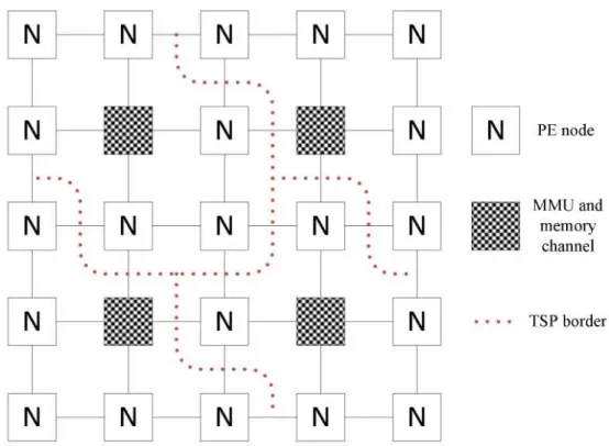
Man et. al [MAN10] discuss the problems of using a unique, centralized Memory Management Unit (MMU), shared by PEs in a NoC-based Chip Multiprocessor (CMP). According to the authors, as the number of PEs increases, the number of memory references also tends to increase. Consequently, the sequential structure of a centralized MMU can become the bottleneck of the system. To tackle this problem, a distributed MMU is proposed. Distributed MMU scheme takes several MMUs as resources on the NoC to handle memory access requests. According to the authors, with a proper number of MMUs and reasonable network placement of these modules, both memory bandwidth requirements and NoC communication traffic may be decreased. In the design proposed by [MAN10], PEs are grouped into a Translation-Sharing Partition (TSP) that contains a MMU responsible for handling requests of PEs belonging to that partition. Figure 3 shows an example of a 5x5 2D mesh NoC having 3 TSPs and 4 MMUs.
Figure 3 – NoC view of TSP partitions and positioning of MMU and PE nodes.
Monchiero et al. [MON06] present a NoC-based MPSoC platform, modeled at the GRAPES Plataform [MON08]. The platform is composed of ARM7 PEs, memory elements, memory and interrupt controllers, as shown in Figure 4. Each PE has a L1 data and instruction cache. Memory elements can be of two types: shared memory banks or a L2 cache, centralized in a unique node connected to the NoC. To access one of the shared banks, a given PE must send a request to a HW Memory Management Unit (HWMMU) that is responsible for managing shared memory access. The operations supported by HWMMU are: memory allocation (MMU_MALLOC); memory release (MMU_FREE); copy and move.
Figure 4 – Multiprocessor architecture proposed by [MON06].
Silva et al. [SIL09] present an evaluation of four different memory organizations for a NoC-based MPSoC to compare their performance and energy efficiency. The evaluated organizations are: (i) a distributed memory that includes processors with local private memories; (ii) a shared memory accessed by all processors; (iii) a distributed shared memory; (iv) a physically shared but logically distributed memory (nDMA). The experiments conducted by the authors evaluate the behavior of the four memory organizations when the traffic on the network increases, what induces higher packet latency. Results showed that for applications with high communication demands, the distributed memory organization presents the highest tolerance to communication latency. Although, applications with low communication workload this organization seems to suffer more than others due to network latency. Regarding performance, the nDMA memory shows the smallest variation of performance reduction (22% to 33%) when NoC traffic increases from 10% to 20%.
2.1.2 Hybrid organizations
elements: a NoC, RISC-like PEs and the Multiprocessor Memory Management Unit (MPMMU) that interfaces an external DDR memory. The NoC has a torus topology and implements a deflection-routing (Hot Potato) algorithm that allows each flit to be routed independently. Each PE consists of a configurable Tensilica XtensaLX, which was used to implement the MPI message passing interface. The MPMMU is a special processor that handles shared-memory transactions (reads/writes). The global shared-memory is divided into two logic segments: shared and private area. Each core has a private segment and can access the shared segment through the use of a lock mechanism. Experiments were conducted by the authors using the use of the Jacobi algorithm. The authors reached the conclusion that the hybrid approach scales better and uses silicon area for additional cores instances in a more efficient way compared to a standard shared memory approach.
2.1.3 Memory organizations comparison
Table 1 shows a comparison of the reviewed works in memory organizations considering four topics. Most works adopt a 2D Mesh NoC. Only one of the reviewed works ([MON06]) evaluates the impact of the NoC topology in the memory performance. Most works consider the evaluation of the proposed platform in SystemC or higher-level simulation platforms. Although high-level models accelerate implementation, they do not provide high accuracy. It is also possible to notice that most works do not evaluate the energy consumption considering the placement of the memory in the MPSoC, and neither evaluate the cost of transactions on the network. This work proposes the exploration of DSM organization, modeled in synthesizable VHDL, where L2 data cache banks characterize the shared memory.
2.2 Cache coherence protocols for NoC-based MPSoCs
Table 1 - Comparison of the reviewed works considering memory organization.
Memory Organizations for NoC-based MPSoCs
Author topology NoC Organization Memory Modeling Level /
Simulator Goal
[KIM06] 2D Mesh Shared Memory L1 and L2 + banks
RSIM
Simulator Decrease latency of the cache coherence protocol
[YUA08] 2D Mesh SM banks + semaphore
memory SystemC
Explore Synchronization and Memory consistency
[MAN10] 2D Mesh Distributed MMU (Memory
Management Unit) -
Evaluate the placement of MMUs
[MON06] spidergon, 2D Ring, Mesh
L1 and L2 + SM
banks Platform Grapes Implement a HWMMU
[SIL09] 2D Mesh DSM, nDMA and 4 types: SM,
private memory SystemC
Evaluate memory performance under latency
[TOT10] Torus L1 + L2 SystemC RTL and Explore a hybrid architecture
This work 2D Mesh L1 + L2 RTL Evaluate DSM and allow data migration algorithm
Cache coherence protocols can roughly be classified in two classes: software-based protocols and hardware-based protocols. Hardware protocols include snoopy-based protocols, which are not appropriate for NoC-based MPSoCs, as they require that all accesses to the memory must be visible for all memory banks and PEs of the system. Global visibility is very efficient for busses, but NoCs are composed of segmented links interconnected through routers. To provide global visibility all memory accesses need to be broadcasted to all processors, considerably increasing the amount of traffic in the NoC. In addition, according to the energy model proposed by Hu et al. [HU03], the amount of traffic in the NoC causes an increase in the energy consumption of the NoC.
Software-based protocols, usually, rely on explicit synchronization, and do not ensure cache coherence on the granularity of individual memory accesses, but on groups of memory accesses. Additionally, software protocols rely on the use of compiled-time information to predict run-time behavior. The performance of such protocols is significantly degraded when predicted hits do not happen at runtime [ADV91].
Yuang et al. [YUA08] proposes a hierarchical cluster based cache coherence protocol for large-scale NoC-based shared memory architectures. The nodes of the NoC are grouped into units named clusters. Each cluster consists of a group of L1 cache banks and one L2 cache bank, which is named HEAD and contains a local directory. The HEAD node is located at a NoC router that has the average minimum distance to all members of the cluster. Figure 5(b) shows a 5x5 mesh NoC, where each circle comprises a cluster. The HEAD of each cluster is painted in black. The shared memory is located off-chip and maintains the global directory, as shown in Figure 5(a). Cache coherence is enforced hierarchically. Similarly to the directory-based cache coherence protocol, the global directory is a flat, full-map directory, which stores the status of each block. The difference is that instead of keeping which PEs have copies of the blocks, the global directory keeps which clusters have a copy of each block. Intra-cluster, the local directory stores which nodes of the cluster (L1 caches) contain a copy of each block.
The advantages of using such protocol for enforcing coherence on the platform is the reduction on the number of hops traversed by messages of the coherence protocol (Longest Manhattan Distance and Long Distance Travel). Another advantage is the reduction on the space required for storing the directory. A disadvantage of the clustered approach is that each application must be mapped onto a single cluster, which is not always possible, what can degrade performance significantly.
Figure 5 – In the left, it is shown the architecture of the HEAD node. In the right, each circle comprises a cluster region [YUA08].
must arrive: (i) at the time of a write-hit, a block appears in shared state with exactly two cached copies and the processor currently requesting the invalidation operation is not the same which requested invalidation previously; (ii) at the time of a write-miss, there is only one copy of this block and it is modified.
By detecting that a given block is migratory, the protocol used to maintain its coherence is the adaptive cache coherence protocol, otherwise a regular version of the invalidate protocol is used. The adaptive protocol reduces execution time of applications and reduces the traffic generated on the NoC by the cache coherence protocol. To evaluate the protocol, experiments were conducted with the use of the RSIM simulator, with sizes of 32KB (2-way associative) for L1 cache and 1MB (4-way associative) for L2 cache, both having block sizes of 32 bytes. Five SPLASH benchmarks were simulated. The results showed that the adaptive protocol performed better in some benchmarks, but worse in others compared to the regular MESI protocol.
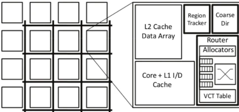
Jerger et al. [JER08b] proposes a method for cache coherence in multicore architectures, named Virtual Tree Coherence (VTC). It is based on a virtual ordered interconnection tree, which keeps a history of nodes sharing a common region of memory. Figure 6 shows the architecture of each node. For each region, a virtual tree of the nodes that shared that region is created. The routers used information stored in the VTC Table (Figure 6) to obtain information about the virtual trees and their members. Every time a given region is accessed by one of the nodes, a request is sent to the root of the tree, which in turn, requests the data to the node holding the most updated copy of it. This request is done through a multicast message traversing the tree.
The implementation of the multicast according to the tree topology decreases latency when compared to unicast-based implementations. The authors compare their implementation to a directory-based implementation and to another implementation based on a greedy algorithm. Results show a performance improvement of 25% of this implementation over the directory-based one and 11% over the greedy one.
[CHT09] present the development of a dynamic hybrid cache coherence protocol for shared-memory NoC-based MPSoCs shown in Figure 7. According to the authors, existing regular protocols such as invalidation and update, do not take into account the patterns of data accesses performed by applications during runtime, leading to unnecessary operations of update/invalidate on a given block. This might affect the amount of traffic on the NoC (e.g. generated by unnecessary update operations) and, consequently, increase the energy consumption. In response to that, the authors propose a protocol based on the traditional directory-based protocol that adapts itself to the way in which the data is used, alternating between an update to invalidate protocol and vice-versa. It is considered as dynamic because the threshold value that determines if the protocol should be alternated changes during runtime. Operations of the cache coherence protocol are transmitted to PEs through the use of a dedicated bus, as shown in Figure 7.
Figure 7 – NoC-based MPSoC architecture with an exclusive bus for cache coherence transactions [CTH09].
The experiments were conducted with the use of the SoCLib platform running two benchmarks: Fast Fourier Transform and matrix multiplication. The simulated architecture is composed by MIPS R3000 processors, containing I-Cache and D-Cache, two banks of shared memory, one for instruction and the other for data. All modules are connected to a crossbar NoC through a VCI interface. Results show that the most significant gain of the hybrid protocol is the reduction on energy consumption when compared to regular invalidate and update protocols. Also, the hybrid protocol reduces both cache misses, compared to invalidation protocol, and unnecessary updates, compared to update protocol. The use of a dedicated bus to cache coherence operations affects the scalability of the system.
SoC architectures, software-oriented cache coherence protocols provide the best trade-off between complexity and performance as they incur no hardware cost at all. The software-solution used in [PET06] makes shared data uncached and local, non-shared data, cached. Each application is written as a set of POSIX threads. The memory is partitioned into two types of segments: local segments, which store private data for each processor and shared segments, which store shared variables such as communication buffers. Memory consistency is guaranteed with the use of the release consistency model. The experiments conducted by the authors compare the proposed solution to a fully uncached solution. The results show a performance improvement of a factor of 3, versus the fully uncached solution when running a Motion-JPEG decoder for 48x48 pixels movies of 24 images. Another software solution for a cache coherence protocol in MPSoCs is presented by Ophelders et. al [OPH09].
Most of the works of the state of the art, shown in Table 2, adopt a shared memory organization and the platform evaluated is usually modeled in high abstraction levels. Some works propose the use of traditional protocols for NoC-based MPSoCs, such as the directory-based protocol. Most NoC-based MPSoCs designs including a memory hierarchy do not explore the services offered by NoCs to improve performance, using the NoC as simple bus. An exception to this remark is the work of [JER08a] which proposes a protocol based on trees implemented in the NoC. Several NoCs implement multicast messages at the physical level [JER08a][CAR08]. The use of multicast messages by cache-coherence protocols has several advantages, as the reduction on the number of cycles required to perform write-invalidate operations, as well as to reduce the traffic generated by these protocols on the NoC.
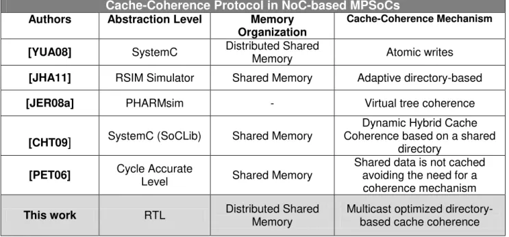
Table 2 - Reviewed works in cache coherence protocol for NoC-based MPSoCs. Cache-Coherence Protocol in NoC-based MPSoCs
Authors Abstraction Level Memory Organization
Cache-Coherence Mechanism
[YUA08] SystemC Distributed Shared Memory Atomic writes
[JHA11] RSIM Simulator Shared Memory Adaptive directory-based
[JER08a] PHARMsim - Virtual tree coherence
[CHT09] SystemC (SoCLib) Shared Memory
Dynamic Hybrid Cache Coherence based on a shared
directory
[PET06] Cycle Accurate Level Shared Memory Shared data is not cached avoiding the need for a coherence mechanism
2.3 Data Migration Algorithms
Wire delays play an important role in cache design [BEC04]. As semiconductor technology advances the number of cycles required to transmit data in the chip increases. Therefore, wire latency increases fast. To reduce this latency in cache design, designers have split L2 caches into several cache banks. Such architectures are named NUCA (Non Uniform Cache Access) and have varying access latency. Latency is a function of the distance between the processor requesting data and the cache bank that will provide the data.
Some of the key design points of data migration algorithms include:
when the migration occurs, which directly influences the way that cache accesses are accounted;
the granularity of the migration, for instance an algorithm could migrate one or more blocks of a cache at once;
which bank (target) will receive the migrating block once detected that the migration should occur;
how blocks are retrieved in the system before and after migration (search algorithm).
Beckmann et al. [BEC04] argue that block migration is less effective for CMPs (chip multiprocessors) because 40-60% of L2 cache hits in commercial workloads are satisfied in central banks, which are equally far from all processors. Based on this assumption, the Authors propose a combined solution which uses a data migration protocol combined with optimized layout techniques. The main goal of their work is to optimize performance. In our work, we consider MPSoC applications, which may not present the same pattern that is present in commercial workloads. Additionally, the main focus of our work, which is not addressed by [BEC04], is the energy consumption of cache accesses.
accesses done by a cluster of PEs reaches a threshold of 4 accesses. Additionally, an algorithm called Active Neighbor Migration is implemented on top of DMA to migrate blocks that will be likely accessed in the future by a group of PEs. A problem in this approach is that applications may not be entirely mapped into a cluster. This may cause the problem of migrating a cache block several times between cache banks due to data sharing between two tasks of the same application.
Figure 8 – Cluster architecture proposed by Nafziger et al. [NAF10].
Eisley et al. [EIS08] propose the use of data cache migration to reduce off-chip memory access. Every time a block is evicted from L1 cache, a migration algorithm uses information embedded in the routers of the NoC to steer the migrating cache blocks towards underutilized L2 caches. The information present in the routers (Score Table in Figure 9) is updated periodically from immediate neighbors and is based on estimates of L2 cache utilization in a particular direction. The authors justify this action by saying that evicted blocks probably will be used in the near future. In this way, a cache miss is avoided. The problem with this approach is that as any L2 cache is eligible for receiving an evicted cache block, evicted blocks may interfere in the performance of other applications.
Figure 9 – Router architecture proposed by Eisley et. al [EIS08] to guide evicted blocks to unused cache blocks.
2.3.1 Static and Dynamic NUCA
NUCA architectures are sub-divided in two categories: NUCA and D-NUCA. In S-NUCA architectures, blocks are mapped to a given cache bank based on its address. The blocks are not moved between cache banks. In D-NUCA cache architectures, a block may be migrated to other banks towards processors that mostly access it, reducing dynamic energy consumption and latency. Despite the benefits of migration, one of the main challenges of D-NUCA cache architectures is to implement an energy-efficient and low latency mechanism to search for a block. It is necessary because as the blocks can migrate from one bank to another, it is not possible to determine the location of a block based only on its address, such as in an S-NUCA.
[LIR11] proposes a search algorithm named HK-NUCA for D-NUCA cache architectures. The algorithm has three stages to find a block in the L2 NUCA cache and is activated after a miss occurs in the first level cache. In the first stage, the cache controller of the requesting core accesses the closest NUCA bank; in the second stage, the home bank is accessed. The home bank corresponds to the bank determined by the bank bits of the address being accessed; and in the third stage, parallel accesses are sent to all banks that possibly hold the block. In case none of the stages finds the block, a miss request is sent to the upper-level memory.
2.3.2 Data Migration Methods Comparison
adopts as the target platform NoC-based MPSoC. Additionally, most of the solutions only optimize the latency accesses, but do not consider the energy consumption. As one of the main goals of MPSoC designs is to consume low energy, our work proposes a data migration protocol whose main goal is to reduce energy consumption after performing a data migration.
Table 3 - Summary of the reviewed for data migration protocols. Data Migration Protocol
Authors Migration Algorithm Goal Platform Communication Infrastructure
[BEC04] Direction Migration
Algorithm Optimize performance CMP 2D Mesh NoC
[NAF10] Direction Migration
Algorithm + Prediction based Migration
Reduce cache access
latency CMP between routers 2D Mesh NoC / Bus between
PEs
[EIS08] Directional Migration
guided by usage information
Reduce off-chip memory
accesses CMP 2D Mesh NoC
[KAN05] Gradual Migration
Algorithm Decrease the number of necessary migrations CMP 2D Mesh NoC
This Work Region based migration Decrease energy
consumption MPSoC 2D Mesh NoC
2.4 General evaluation of the state of the art
Most papers consider the modeling of the platform in cycle-accurate level or higher-levels of abstraction. Although these models require less effort and allow faster simulation, the RTL level still must be considered. The RTL level is necessary because some problems, concerning either the memory architecture or the traffic generated on the NoC are only observable at this level or at lower abstraction levels. Common examples of these problems are: congestion, burstiness and jitter.
3 HEMPS-Q PLATFORM
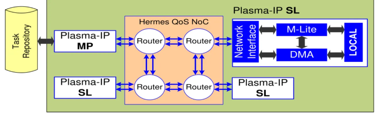
The HeMPS-Q Platform, developed in the scope of Carara’s Thesis [CAR11] (Figure 10), is a homogeneous MPSoC in which PEs are interconnected through a Network-on-Chip (NoC) named Hermes QoS. Each PE contains a RISC microprocessor, a local (scratch pad) memory, a DMA controller and a Network Interface (NI). These modules are wrapped by the Plasma-IP module, which is then connected to the NoC. The next sections detail each of these modules. Section 3.6 presents the microkernel responsible for managing task allocation/execution and communication on the system. Concluding this Chapter, Section 3.8 presents the HeMPS Generator framework, which allows automatic generation of a parameterized architecture at RTL level. The user can manually configure platform parameters, such as NoC size, memory size and number of memory pages.
Hermes QoS NoC
Router Router Router Router Plasma-IP SL Plasma-IP MP N et w ork In te rfa ce
Plasma-IP SL
M-Lite DMA Ta sk R ep osi to ry LO C A L Plasma-IP SL
Figure 10 – HeMPS-Q platform architecture.
There are two types of Plasma-IPs: slaves (SL) and master (MP). Plasma-IP SLs are responsible for executing application tasks. Plasma-IP MP is responsible for managing task mapping and system debug. The external memory, named task repository, contain all application tasks. According to some mapping heuristic, the Plasma-IP MP maps the tasks into the Plasma-IP SLs. The Plasma-IP MP can also receive debug messages from Plasma-IP SLs, transmitting them to an external host through an Ethernet interface (not shown in Figure 10).
3.1 Hermes QoS
3.1.1 Hamiltonian routing
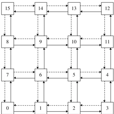
According to [HAR72], it is possible to define several Hamiltonian paths on a bi-dimensional mesh by labeling the routers from 0 to N-1, being N the number of routers, as shown in Figure 11. A Hamiltonian path is a path through which it is possible to traverse all nodes of a graph passing only once for each node. After defining the Hamiltonian paths, the network can be divided into two disjoint and acyclic sub-networks, as defined by the dual-path algorithm. One sub-network contains ascending paths that go from the smallest label router to the highest label router and the other contains descending paths that go from the highest label router to the smallest label router. Thus, packets sent from a router labeled 0 targeting a router labeled 3 will take the ascending path. Figure 11 shows a network with 16 routers, labeled from 0 to 15, having two disjoint networks. Ascending packets are sent using the network depicted by the lines, whilst descending packets are sent using the network depicted by the dotted lines.
7 6 5 4
0 1 2 3
15 14 13 12
8 9 10 11
Figure 11 - Example of label assignment based on a Hamiltonian path in a 4x4 mesh. Hamiltonian paths provide a good support for implementing efficient multicast/broadcast algorithms [CAR08]. Multicast messages may be used in the implementation of cache coherence protocols to optimize invalidation messages that target several PEs caching a given block. Without multicast, an invalidation message would have to be sent individually to all processors in the system, increasing the number of transactions in the network, as well as energy consumption and congestion. Thus, it is possible to assert that the interconnection mean plays an important role on the design and implementation of a cache coherence protocol.
message is sent from a lower labeled router to a higher labeled router, the target network addresses are sorted in decreasing order, as shown in Figure 12(b). On the other hand, when a multicast message is sent from a higher labeled router to a lower labeled router, network addresses are sorted in increasing order in the header, as shown in Figure 12(a). When the message reaches each target router, the address of the current address (first flit of the header) is removed from the header and a copy of the message is forwarded to the next network address present in the header, and to the local port of the router.
Figure 12 – Two examples of multicast messages. The first shows an example of a multicast message to network addresses 8, 10, 12 and 14. The second shows a multicast
message that target network addresses 5, 3 and 1. 3.1.2 Physical channels and priority
The NoC Hermes QoS uses two 16-bit channels (physical links) to interconnect the routers. The advantage of this approach is that it allows allocation of one physical path for sending only high priority packets. In the NoC Hermes, channel 0 is used to transmit both high and low priority packets, whilst channel 1 only transmits high priority packets.
3.2 Plasma-IP
Plasma-IP is a modified version of an open-source soft core, described in VHDL, freely available at OpenCores [OPE11]. It consists of a 32-bit RISC architecture, strongly based on the MIPS-I ISA (Instruction Set Architecture).
The Plasma-IP core is implemented with a configurable pipeline that can be set to two or three stages, with an additional optional stage for memory accesses. The entity that controls the core converts a 32-bit instruction opcode to a 60-bit opcode and sends control signals to the other entities.
3.3 Network Interface (NI)
The Network Interface main function is to serve as a wrapper of the Plasma processor to the NoC. It is responsible for splitting 32-bit words that are written in the memory by the processor to 16-bit flits that are transmitted in the NoC. So, for every word sent from the processor to the network, two flits are sent through the NoC. The NI is responsible for breaking up words into flits and re-assembling the words at the receiving end.
The NI is constituted by two finite-state machines (FSM): Receive and Send. The Receive is a 4-state machine responsible for buffering incoming packets from the network and signaling to PLASMA that a new packet may be handled. Furthermore, the Receive machine is responsible for controlling the reading of data from Plasma core. The Send is a 6-state machine responsible for sending packets to the NoC. The contents of the packets sent on the NI are fetched from memory by the DMA module. The NI controls DMA operations, and copy to/from memory.
3.4 DMA
The implementation of the Plasma processor available at OpenCores did not include a DMA module in its architecture. Without a DMA module, the processor must handle incoming packets buffered at NI. This operation is very expensive for the processor as it cannot execute any application task during this time, which causes a reduction on the system performance.
To address this problem, a DMA module was designed to execute two operations: transfer packets stored on memory to the NI and transfer incoming packets from NI to memory. DMA programming is done inside the microkernel (Section 3.6), whenever a new interrupt event originated from the NI module is detected or, every time a packet must be sent to the NoC. The configuration of the DMA module is done through a set of memory-mapped registers:
DMA_OP: defines the operation to be performed by the DMA module, and can be either read or write.
DMA_ADDRESS: defines the initial address for a given operation.
DMA_SIZE: defines the size of the data to be transferred.
DMA_START: initiates the operation assigned to the DMA.
3.5 Memory system
Each Plasma-IP follows the Von-Neumann organization, having only one private memory, which stores both data and instructions. To allow simultaneous access from DMA and processor, the private memory is implemented as a dual-port memory. The memory space is divided into pages. The first pages store the microkernel, and the remaining ones store application tasks.
Application tasks are fetched from an external, off-chip memory, during system initialization (static mapping) or at run-time (dynamic mapping). The master PE accesses the external memory through a repository interface, in order to fetch object code of all tasks that are going to be executed in the system. This interface is also present on slave Plasma-IPs, and can be used to connect the core to another type of memory, such as a cache memory, with the advantage of not having to modify the core architecture.
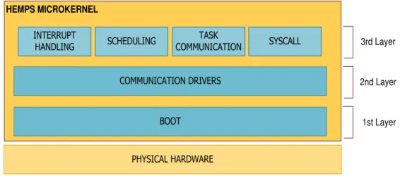
3.6 Microkernel
The microkernel that runs on PLASMA core is a tiny operating system responsible for managing and supporting task execution on each core. The HeMPS microkernel is a preemptive OS, where each task occupies the CPU for a pre-defined period of time called timeslice. The microkernel has two versions: one runs on PLASMA master whose main objective is to coordinate task distribution and management. The master does not run any application task. The other runs on PLASMA slaves and gives support to features such as multitasking and software interrupts (traps). The memory of both master and slave is paginated. The kernel occupies the first pages, whilst the tasks occupy the remaining ones. The microkernel is divided into layers as shown in Figure 13.
PHYSICAL HARDWARE BOOT
COMMUNICATION DRIVERS INTERRUPT
HANDLING SCHEDULING
TASK
COMMUNICATION SYSCALL HEMPS MICROKERNEL
1st Layer 2nd Layer 3rd Layer
Figure 13 - HeMPS Microkernel Layers.
3.6.1 Boot (1st Layer)
The boot layer contains a few routines written in assembly and in C. The assembly code is responsible for initializing segments of global and static (.bss) data, global and stack pointers.
The Plasma processor starts its execution by fetching an instruction from the first address in memory (0x00000000). The first positions of memory contain the assembly code.
3.6.2 Communication drivers (2nd Layer)
The communication drivers are accessed only inside kernel address space, preventing user tasks from dealing directly with hardware modules. Although this limitation exists, a user task can have access to communication drivers through high-level macros, defined in the microkernel, which cause a trap and call to the communication driver routines. The communication routines are Send() and Receive(). Both routines write/read messages from the pipe (communication vector, described in Section 3.6.7). The implementation of the communication model in the HeMPS Platform is based on the read request protocol, while the computation model is based on the KPNs (Kan Process Networks). The Receive() blocks task executes until the moment that the message to be received is available on the pipe, the Send() routines is non-blocking.
3.6.3 Task execution (3rd layer)
To manage tasks execution, the microkernel keeps a TCB (Task Control Block) structure for each task. This structure contains the entire context of each task, so that it must be updated before switching execution to another task (context saving). Figure 14 shows the TCB structure that is currently implemented inside the microkernel in C. The registers saved on TCB structure are: temporary registers ($t0 - $t9); saved registers ($s0 - $s8); argument registers ($a0 - $a3); function result registers ($v0 - $v1); return address ($ra); stack pointer ($sp); global pointer ($gp); and registers used to store multiplication/division results ($hi and $lo). Beyond these registers, for each task is maintained its id (identifier), pc (program counter), offset (indicating its initial memory position) and status. The status of a task can be:
READY : means that the task is ready to be executed;
RUNNING : indicates that the task is currently executing in the CPU;
TERMINATED : indicates that the task finished its execution;
WAITING : indicates that the task requests a message and is waiting for response;
FREE : indicates that the TCB is free and can be allocated;
Figure 14 - TCB structure described in C language. 3.6.4 Multitasking
Preemptive multitasking requires support from the hardware, otherwise there might exist situations where it is not possible to remove a given task from the CPU. The PLASMA core maintains a memory-mapped tick counter, implemented as an internal memory-mapped register. This register is incremented each clock cycle, and causes an interrupt event when it reaches a threshold. The time interval that starts at zero and the moment when the counter reaches the threshold is denominated timeslice. The interrupt event is handled by the interrupt handler, which in turn, calls the scheduling algorithm that allocates another task to be executed in the CPU.
The microkernel implements a round-robin scheduling algorithm, which assigns time slices for each task in equal portions and in circular order, handling all tasks without priority. Round-robin scheduling is both simple to implement and starvation-free.
3.6.5 Task allocation
The master PE, according to the task mapping, executes task allocation on HeMPS Platform. HeMPS Platform supports two types of task mappings:
Static: The user defines, at design time, in which Plasma-IP each task is going
to be executed. When the execution starts, tasks are sent to PEs according to the user definition.
Dynamic: When a task is dynamically allocated, it is sent to the Plasma-IP that
will execute it only when another task in the system requests the allocation. This situation happens whenever a task Ti, running on processor Pi, needs to
send a message to task Tj. Task Ti searches for task Tj location on its internal
table, but it finds out that task Tj has not been allocated yet. Consequently, it
sends a message to the master requesting the allocation to be done. 3.6.6 Interrupts
When a hardware interrupt event happens, the PC register receives the 0x3C address causing the execution of a full context saving function. When a software interrupt event happens, the PC register receives the 0x44 address causing the execution of a partial context saving function.
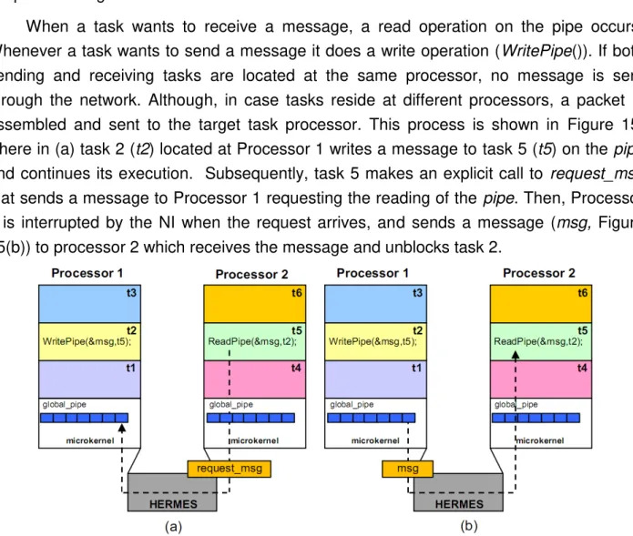
3.6.7 Task communication
Different tasks running on a distributed system need to communicate to coordinate and synchronize task execution. Task communication inside the processor is done through an area called pipe. A pipe is a communication channel in which messages are consumed at the same order they were produced. There exists only one global pipe per processor that is shared between all tasks.
According to the KPN model adopted by HeMPS microkernel, a channel read operation must be blocking. Thus, when a Receive() instruction is executed, the task is blocked until it receives the requested message from the pipe. On the opposite, write operations must be non-blocking, which means that after every Send() operation, the task keeps executing.
When a task wants to receive a message, a read operation on the pipe occurs. Whenever a task wants to send a message it does a write operation (WritePipe()). If both sending and receiving tasks are located at the same processor, no message is sent through the network. Although, in case tasks reside at different processors, a packet is assembled and sent to the target task processor. This process is shown in Figure 15, where in (a) task 2 (t2) located at Processor 1 writes a message to task 5 (t5) on the pipe and continues its execution. Subsequently, task 5 makes an explicit call to request_msg that sends a message to Processor 1 requesting the reading of the pipe. Then, Processor 1 is interrupted by the NI when the request arrives, and sends a message (msg, Figure 15(b)) to processor 2 which receives the message and unblocks task 2.
3.7 Memory management
As already mentioned in section 3.5, each Plasma-IP contains only a dual-port private memory, which is divided into pages. The first pages store the microkernel, and the subsequent ones store user tasks. Each task is associated to a page number, which is kept by a CPU internal register, denominated page. Every memory address (mem_address_wop) generated by memory controller (Mem_ctrl) of the Plasma core does not includes the page, only the logical offset inside it. Thus, before putting the address on the memory bus, it is necessary to concatenate the page initial address in memory with the address contained in mem_address_wop.
This mechanism prevents a given task located at a given page to access data from a task located at a different page. An important consideration is that this mechanism also prevents tasks from accessing the kernel memory area, avoiding a crash caused by a malicious user task.
3.8 HeMPS Generator
![Figure 5 – In the left, it is shown the architecture of the HEAD node. In the right, each circle comprises a cluster region [YUA08]](https://thumb-eu.123doks.com/thumbv2/123dok_br/16656497.211563/28.892.145.740.771.934/figure-shown-architecture-head-circle-comprises-cluster-region.webp)
![Figure 7 – NoC-based MPSoC architecture with an exclusive bus for cache coherence transactions [CTH09]](https://thumb-eu.123doks.com/thumbv2/123dok_br/16656497.211563/30.892.273.669.425.731/figure-based-mpsoc-architecture-exclusive-cache-coherence-transactions.webp)
![Figure 9 – Router architecture proposed by Eisley et. al [EIS08] to guide evicted blocks to unused cache blocks](https://thumb-eu.123doks.com/thumbv2/123dok_br/16656497.211563/34.892.229.694.95.432/figure-router-architecture-proposed-eisley-evicted-blocks-unused.webp)