Efficient Hardware Design and
Implementation of AES Cryptosystem
PRAVIN B. GHEWARI1 MRS. JAYMALA K. PATIL1 AMIT B. CHOUGULE2 1Department of Electronics & Telecommunication
2
Department of Computer Science & Engineering Bharati Vidyapeeth College of Engineering, Kolhapur, Maharashtra.
Abstract
We propose an efficient hardware architecture design & implementation of Advanced Encryption Standard (AES)-Rijndael cryptosystem. The AES algorithm defined by the National Institute of Standard and Technology (NIST) of United States has been widely accepted. The cryptographic algorithms can be implemented with software or built with pure hardware. However Field Programmable Gate Arrays (FPGA) implementation offers quicker solution and can be easily upgraded to incorporate any protocol changes. This contribution investigates the AES encryption and decryption cryptosystem with regard to FPGA and Very High Speed Integrated Circuit Hardware Description language (VHDL). Optimized and Synthesizable VHDL code is developed for the implementation of both 128- bit data encryption and decryption process. Xilinx ISE 8.1 software is used for simulation. Each program is tested with some of the sample vectors provided by NIST and output results are perfect with minimal delay. The throughput reaches the value of 352 Mbit/sec for both encryption and decryption process with Device XCV600 of Xilinx Virtex Family.
Keywords: Advanced Encryption Standard (AES), Rinjdael, Cryptography, FPGA, Throughput.
1. Introduction:
To protect the data transmission over insecure channels two types of cryptographic systems are used: Symmetric and Asymmetric cryptosystems. Symmetric cryptosystems such as Data Encryption Standard (DES) [1], 3 DES, and Advanced Encryption Standard (AES) [4], uses an identical key for the sender and receiver; both to encrypt the message text and decrypt the cipher text. Asymmetric cryptosystems such as Rivest-Shamir-Adleman (RSA) & Elliptic Curve Cryptosystem (ECC) uses different keys for encryption and decryption. Symmetric cryptosystem is more suitable to encrypt large amount of data with high speed.
To replace the old Data Encryption Standard, in Sept 12 of 19997, the National Institute of Standard Technology (NIST) required proposals to what was called Advanced Encryption Standard (AES). Many algorithms were presented originally with researches from 12 different nations. Fifteen algorithms were selected to the Round one. Next five were chosen to the Round two. Five algorithms finalized by NIST are MARS, RC6, RIJNDAEL [2], SERPENT and TWOFISH [3]. On October 2nd 2000, NIST [4] has announced the Rijndael algorithm is the best in security, performance, efficiency, implement ability, & flexibility. The Rijndael algorithm was developed by Joan Daemen of Proton World International and Vincent Rijmen of Katholieke University at Leuven.
AES encryption is an efficient scheme for both hardware and software implementation. As compare to software implementation, hardware implementation provides greater physical security and higher speed. Hardware implementation is useful in wireless security like military communication and mobile telephony where there is a greater emphasis on the speed of communication. Most of the work has been presented on hardware implementation of AES using FPGA [5-9]. This paper presents efficient hardware architecture design & implementation of AES using FPGA and describes performance testing of Rijndael algorithm.
The paper is organized as follows. Section 2 describes AES algorithm in brief. Section 3 focuses efficient FPGA implementation of AES. The experimental results are given in Section 4. Finally Section 5 ends up with conclusion.
2. AES Algorithm:
192 or 256 bits (Key length). In this implementation we set the key length to 128. Hence Nk = Key length/32 = 4.
2.1 Encryption Process:
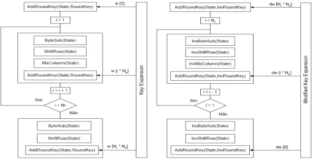
The Encryption and decryption process consists of a number of different transformations applied consecutively over the data block bits, in a fixed number of iterations, called rounds. The number of rounds depends on the length of the key used for the encryption process. For key length of 128 bits, the number of iteration required are10. (Nr = 10). As shown in Fig. 1, each of the first Nr-1 rounds consists of 4 transformations: SubBytes(), ShiftRows(), MixColumns() & AddRoundKey().
Fig. 1 Rinjdael Encryption and Decryption Process
The four different transformations are described in detail below.
Sub Bytes Transformation: It is a non-linear substitution of bytes that operates independently on each byte of the State using a substitution table (S box). This S-box which is invertible is constructed by first takingthe multiplicative inverse in the finite field GF (28) with irreducible polynomial m(x) = x8 + x4+ x3 + x + 1. The element {00} is mapped to itself. Then affine transformation is applied (over GF (2)).
Shift Rows Transformation: Cyclically shifts the rows of the State over different offsets. The operation is almost the same in the decryption process except for the fact that the shifting offsets have different values.
Mix Columns Transformation: This transformation operates on the State column-by-column, treating each column as a four-term polynomial. The columns are considered as polynomials over GF (28) and multiplied by modulo x4 + 1 with a fixed polynomial a(x) = {03} x3+ {01} x2+ {02} x.
Add Round Key Transformation: In this transformation, a Round Key is added to the State by a simple bitwise XOR operation. Each Round Key consists of Nb words from the key expansion. Those Nb words are each added into the columns of the State. Key Addition is the same for the decryption process.
Key Expansion: Each round key is a 4-word (128-bit) array generated as a product of the previous round key, a constant that changes each round, and a series of S-Box lookups for each 32-bit word of the key. The Key schedule Expansion generates a total of Nb (Nr + 1) words.
The decryption process is direct inverse of the encryption process. All the transformations applied in encryption process are inversely applied to this process. Hence the last round values of both the data and key are first round inputs for the decryption process and follows in decreasing order.
3. Efficient Implementation of AES:
bits slices for a total 6912 CLB slices. The XCV600 is fast, high-density Field-Programmable Gate Arrays with 661,111 system gates.
3.1 Encryption Implementation:
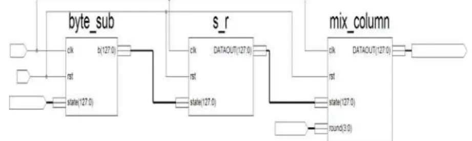
VHDL is used as the hardware description language because of the flexibility to exchange among environments. The software used for this work is Xilinx ISE 8.1. This is used for writing, debugging and optimizing efforts, and also for fitting, simulating and checking the performance results using the Xilinx xst simulation tools available on Web pack design software. An iterative method of design is implemented to minimize the hardware utilization. The encryption process is shown in figure 3. In order to allow a full parallel process of the state, it is necessary to implement all the transformations over 128 bits. The most expensive one is the Byte substitution, because it is a table lookup operation.
Fig. 2 Block Diagram of Encrypt Module
Fig. 3 Block Diagram of complete Encryption Process
3.2 Decryption Implementation:
The decryption implementation results are similar to the encryption implementation. The key expansion module is modified in the reverse order. In which last round key is treated as the first round and decreasing order follows. The complete decryption process is shown in figure 4.
4. Experimental Results:
All the results are based on simulations from the Xilinx ISE tools, using Test Bench Waveform Generator. All the individual transformation of both encryption and decryption are simulated using FPGA Vertex family and Xcv600 device. Each program is tested with some of the sample vectors provided by NIST [4].
4.1. Simulation Results:
Figure 5 shows the waveforms generated by the 128-bit byte substitution transformation. The inputs are clock of 220ns time period, Active High reset, and128-bit state as a standard logic vector, whose output is128-bit S-box lookup substitution.
Fig. 5. Simulation Waveforms of 128-bit Byte Substitution
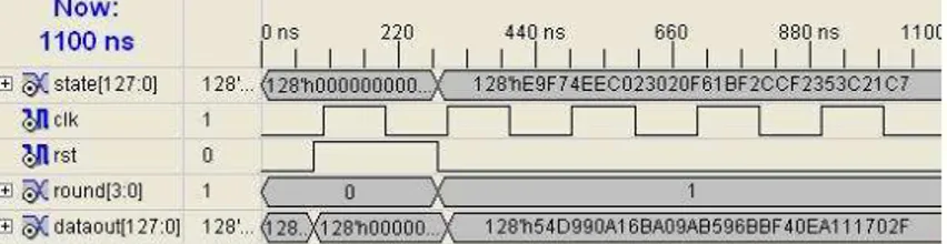
Figure 6 represents the waveforms generated by the 128-bit shiftrow transformation. The inputs are clock of 240ns time period, Active High reset, and 128-bit state as a standard logic vector.
Fig.6 Simulation Waveforms of Shift Row Transformation
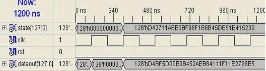
Figure 7 illustrate the waveforms generated by the 128-bit Mix Columns transformation. The inputs are clock of 240ns time period, Active High reset, and 128-bit state.
Fig.7 Simulation Waveforms of Mix Column Transformation
The waveforms generated by the 128-bit Add Round Key operation are shown in fig.8. The inputs are clock of 100ns time period, 128-bit key and 128-bit state as a standard logic vector, whose output is the 128-bit which is EXOR operation of 128-bit state and 128-bit key.
Fig. 8 Simulation Waveforms of Add Round Key
Fig. 9 Simulation Waveforms of Key Expansion
Encryption Process (Cipher):
AES block length/Plane Text = 128bits (Nb=4)
Key length = 128 bits (Nk =4); No. of Rounds = 10(Nr =10) Plane Text : 00112233445566778899aabbccddeeff Key : 000102030405060708090a0b0c0d0e0f Output/Cipher Text: 69c4e0d86a7b0430d8cdb78070b4c55a
Figure 10 represents the waveforms generated by the 128-bit complete encryption Process. The inputs are clock1 & clock2, Active High reset, 4-bit round, and 128-bit state & key as a standard logic vectors, whose output is the 128-bit cipher (encrypted) data.
Fig. 10 Simulation Waveforms of Final Round of Encryption Process
Figure 11 shows the waveforms generated by the128-bit inverse byte substitution transformation. The inputs are clock of 120 ns time period, Active High reset, and bit state as a standard logic vector, whose output is 128-bit Inverse S-box lookup substitution.
Fig. 11 Simulation Waveforms of 128-bit Inverse Byte Substitution
Figure 12 represents the waveforms generated by the 128-bit inverse shiftrow transformation. The inputs are clock of 120 ns time period, Active High reset, and 128-bit state.
Fig. 12 Simulation Waveforms of Inverse Shift Row Transformation
Fig. 13 Simulation Waveforms of Inverse Mix Column Transformation
Decryption Process (Inverse Cipher):
AES block length/Cipher Text = 128bits (Nb=4)
Key length = 128 bits (Nk =4); No of Rounds = 10(Nr =10) Input /Cipher Text: 69c4e0d86a7b0430d8cdb78070b4c55a Key : 000102030405060708090a0b0c0d0e0f Output/Plain Text: 00112233445566778899aabbccddeeff
Figure 14 represents the waveforms generated by the 128-bit complete decryption Process. The inputs are clock1 & clock2, Active High reset, 4-bit round, and 128-bit state & key as
standard logic vectors, whose output is the 128-bit plain text (decrypted data).
Fig14. Simulation Waveforms of Final Round of Decryption Process4.2 Synthesis Results:
The synthesis & mapping results of AES design are summarized in Table1.
Target FPGA Device Virtex XCV600 BG 560– 6
Optimization Goal Speed Maximum Operating Frequency 140.390MHz
Number of Slices 1853 out of 6912 (26%) Number of Slice Flip Flops 512 out of 13824 (3%) Number of 4 input LUTs 3645 out of 13824 (26%) Number of bonded IOBs 391 out of 408 (95%)
Number of GCLKs 2 out of 4 (50%)
256x8-bit ROM 20
Encryption/Decryption Throughput 352 Mbits/sec
Total memory usage 130248 kilobyte
Table 1 Results of FPGA Implementation of AES
The parameter that compares AES candidates from the point of view of their hardware efficiency is Throughput [12].
Encryption/Decryption Throughput = block size frequency/total clock cycles. Thus, Throughput = 128 x 140.390MHz/51 = 352 Mbits/sec.
6. References:
[1.] Nation Institute of Standards and Technology (NIST), Data Encryption Standard (DES), National Technical Information
Service, Sprinfgield, VA 22161, Oct. 1999.
[2.] J. Daemen and V. Rijmen, “AES Proposal: Rijndael”, AES Algorithm Submission, September 3, 1999
[3.] J. Nechvatal et. al., Report on the development of Advanced Encryption Standard, NIST publication, Oct 2, 2000.
[4.] FIPS 197, “Advanced Encryption Standard (AES)”, November 26, 2001
[5.] K. Gaj and P. Chodowiec, Comparison of the hardware performance of the AES candidates using reconfigurable hardware, in
The Third AES Candidates Conference, printed by the National Institute of Standards and Technology.
[6.] H. Kuo and I. Verbauwhede, “Architectural Optimization for a 1.82 Gbits/ sec VLSI Implementation of the AES Rijndael
Algorithm,” Proc. CHESS 2001.
[7.] K. Gaj and P. Chodowiec, “Fast Implementation and Fair Comparison of the Final Candidates for Advanced Encryption Standard
Using Field Programmable Gate Arrays,” Proc. RSA Security Conf., Apr. 2001.
[8.] A. Dandalis, V.K. Prasanna, and J.D.P. Rolim, “A Comparative Study of Performance of AES Final Candidates Using
FPGAs,” Proc. Third Advanced Encryption Standard (AES) Candidate Conf., Apr. 2000.
[9.] Piotr Mroczkowski, Military University of Technology, Poland,“Implementation of the block cipher Rijndael using Altera
FPGA.”
[10.]I. M. Verbauwhede, P.R. Schaumont, and, H. Kuo, "Deign and Performance Testing of a 2.29 Gb/s Rijndael Processor," IEEE J. of Solid State-Circuit, Vol.38, No. 3, March 2003, pp. 569 – 572.
[11.]Xilinx, Inc.,"Virtex 2.5 V Field Programmable Gate Arrays," http://www. xilinx.com.
[12.]A. J. Elbirt, W. Yip, B. Chetwynd, C. Paar, "An FPGA implementation and performance evaluation of the AES block cipher