ISSN : 0975-3397 Vol. 3 No. 9 september 2011 3207
AN ADIABATIC APPROACH FOR LOW
POWER FULL ADDER DESIGN
Praveer Saxena
Department of Electronics & Communication Engineering Accurate Institute of Management & Technology
Greater Noida, India praveer82@gmail.com
Prof. Dinesh Chandra
Department of Electronics & Communication Engineering J.S.S. Academy of Technical Education
Noida, India dinesshc@gmail.com
Sampath Kumar V
Department of Electronics & Communication Engineering J.S.S. Academy of Technical Education
Noida, India sampath_sams@yahoo.com
Abstract— Over the past decade, several adiabatic logic styles have been reported. This paper deals with
the design of a 1-bit full adder using several adiabatic logic styles, which are derived from static CMOS logic, without a large change. The full adders are designed using 180nm technology parameters provided by predictive technology and simulated using HSPICE. The full adders designed are compared in terms of average power consumption with different values of load capacitance, temperature and input frequency. The different designs of full adder are also compared on the basis of propagation delay exhibit by them. It is found that, full adders designed with adiabatic logic styles tends to consume very low power in comparison to full adder designed with static CMOS logic. Under certain operating conditions, one of adiabatic designs of full adder achieves upto 74% power saving in comparison to the full adder designed with static CMOS logic.
Keywords- Adiabatic Logic, Low Power, Energy Recovery, Full Adder.
I. INTRODUCTION
In modern applications, like portable devices, energy has become an important concern: as end users require smaller devices with longer battery life, energy dissipation and fabrication space can be considered as critical concern. The main source of power dissipation in digital circuits is the dynamic power. Several methods to reduce the power dissipation have been reported. One of the methods to reduce the dynamic power dissipation is the circuits based on adiabatic logic. The logic circuits based on adiabatic logic are gaining prime importance due to their low power dissipation characteristic.
Adiabatic logic reduces the energy dissipation by reducing the dissipation across resistances of conducting MOSFETs and recovering the part of energy given to the output back to the source, which extends the battery life. Several adiabatic logic styles have been reported by different authors in their research work [1], [5], [6], [7], [9], [10], [11], [12], [13], [14].
ISSN : 0975-3397 Vol. 3 No. 9 september 2011 3208 input frequency. Beside this, full adders are also compared on the basis of propagation delay exhibit by each full adder.
II. ADIABATIC CHARGING
A) Conventional Charging
The dominant factor of power dissipation in a conventional CMOS device is the dynamic power required to charge and discharge the capacitive nodes within the circuit [1]. To charge the node capacitance CL from a dc
supply of potential VDD, an energy E = CLVDD2 is withdrawn from supply. Only half of this energy is
temporarily stored in capacitor CL. The remaining 0.5CLVDD2 is dissipated as heat in the on resistance of PMOS.
When input becomes logic high, the NMOS turns on and energy stored on capacitor CL is discharged to the
ground and dissipated as heat. Hence during a complete charge- discharge cycle, the energy E = CLVDD2 is
withdrawn from power supply and is dissipated as heat. Half of this energy is dissipated during charging and half is dissipated during discharging.
B) Adiabatic Charging
In static CMOS logic, the abrupt application of supply voltage gives rise to high potential across the switching device. The energy dissipation during charging and discharging can be minimized to a great effect by ensuring that the potential across switching device is kept sufficiently small. Adiabatic charging may be achieved by charging the capacitor from a time varying source that starts at 0V. This time varying source rises towards V at a slow rate that ensures that potential across switching device is kept arbitrarily small. The adiabatic charging is shown in figure 1.
Figure 1. Adiabatic Charging
In fact the energy dissipated across the resistance, R is
Ediss = I2RT = (RC/T) CVDD2 (1)
From the above equation (1), we can see that if T >> RC, the energy dissipation during charging Ediss ≈ 0.
Same is applicable during discharge process.
In addition to this, in some adiabatic logics, the energy dissipation also occurs due to threshold voltage of MOSFET and diode cut-in voltage.
The energy dissipation due to threshold voltage Vt is
E = 0.5CVt2 (2) The energy dissipation due to diode cut-in voltage Vd is
E = CLVd Vs (3)
Where, Vs is the voltage swing.
III. ADIABATIC LOGIC FAMILES
ISSN : 0975-3397 Vol. 3 No. 9 september 2011 3209
A. Adiabatic Dynamic CMOS Logic
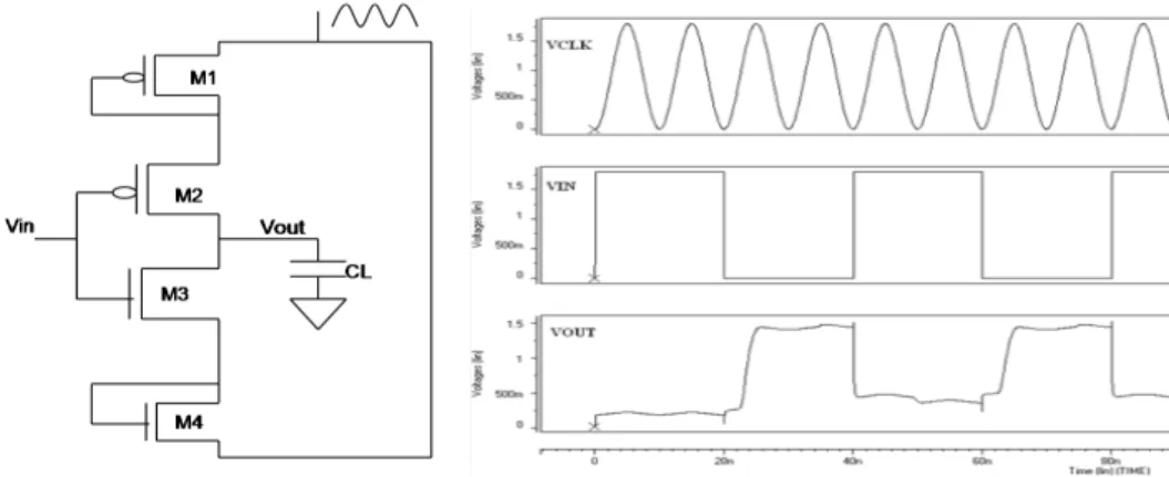
ADCL logic was actually proposed by Takahashi and Mizunuma [7], but later on Modified ADCL logic was given by Kaishita et al [5]. Basic difference between them was the placement of rectifying diode. The modified ADCL logic gives us chance to reduce the number of diodes to implement logic. We have used the Modified ADCL logic in our design. It uses one sinusoidal or triangular clock supply in order to achieve a low energy system. It uses two rectifying diodes, one each in charging path and discharging path to control the charge flow. We have used MOSFET as diode by shorting gate and drain of mosfet together. The sources that may cause energy dissipation in this logic family are threshold voltage of mosfet or potential drop between drain and source of conducting MOSFETs, diode cut in potential and energy dissipated in resistance of MOS devices. The use of slowly varying power clock ensures the small energy dissipation across the ON resistance of MOS devices.
The problem associated with this logic family is the delay. The propagation delay in this logic family depends on period/frequency of power clock. Beside the delay problem, it also requires a load capacitor to hold the output. The schematic of an inverter using this logic family along with resulting waveforms after simulation is shown in figure 2.
Figure 2. ADCL Inverter and waveforms obtained from Simulation.
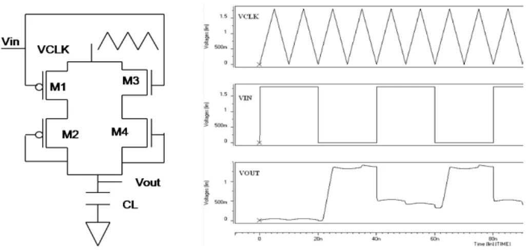
B. Two Phase Drive Adiabatic Dynamic CMOS Logic
The problems associated with ADCL family are solved by Takahashi et al [14]. They presented a new logic family named as two phase drive adiabatic dynamic CMOS logic. It uses two clocks as power supplies with 180° phase difference between them. The supply waveform consists of two modes, “evaluation” and “hold”. When Vclk and Vclkare in evaluate mode, there is conducting path in either PMOS devices or NMOS devices. Output node may evaluate from low to high or from high to low or remain unchanged .When Vclk and Vclkare in hold mode, output node holds its value in spite of the fact that Vclk and Vclkare changing their values. Circuit nodes are not necessarily charging and discharging every clock cycle, reducing the switching activity. Therefore, the speed of 2PADCL circuits is faster than ADCL circuits [14]. The energy dissipation in this logic family occurs due to threshold voltage of MOSFET or potential drop between drain and source of conducting MOSFETs, diode cut in potential and energy dissipated in resistance of MOS devices. The use of slowly varying power clocks ensures the small energy dissipation across the ON resistance of MOS devices. The schematic of an inverter using this logic family and along with resulting waveforms after simulation is shown in figure 3.
ISSN : 0975-3397 Vol. 3 No. 9 september 2011 3210 The problem associated with logic family is lack of robustness as a result of floating output associated with alternate hold phases in operation [5].
C. Glitch Free and Cascadable Adiabati c Logic(GFCAL)
This logic family was proposed by Reddy et al [11]. This logic family can be easily cascaded without any glitch and can be operated by a single power source, and also do not need multi-phase clocks [11]. It uses a single triangular waveform as power clock and employs rectifying diodes in charging path as well as discharging path, so that ripples does not occur and it becomes suitable for cascadable operations. Like other families discussed here, we have used MOSFET as diode by shorting gate and drain of MOSFET together.
The sources of power dissipation in GFCAL logic family are threshold voltage of MOSFET or the potential drop between drain and source of conducting MOSFETs, diode cut-in voltage and dissipation in resistance offered by the pmos and nmos network while charging and discharging of load capacitance respectively. The use of slowly varying power clock ensures the small energy dissipation across the ON resistance of MOS devices. The schematic of an inverter using this logic family and along with resulting waveforms after simulation is shown in figure 4.
Figure 4. GFCAL Inverter and waveforms obtained from Simulation.
The main problem associated with it is, the delay. Like ADCL, it also employs single power clock, so propagation delay in this logic family is also dependent on frequency or time period of power clock.
D. Two Phase Clocked Adiabatic Static CMOS Logic(2PASCL)
In the logic families which include diode in charging path suffer from output amplitude degradation. To deal with this problem, Anuar et al proposed a new logic family named as two phase clocked adiabatic static CMOS logic [9], [10]. This logic family does not include diode in charging path, so that output amplitude degradation does not occur. The 2 phase clocked adiabatic static cmos logic uses a two phase clocking split level sinusoidal power supply. One is in phase while the other is inverted. The voltage level of Vclk exceeds that of Vclk by VDD/2. By using these two split – level sinusoidal waveforms, which have peak to peak voltages of 0.9V, the
voltage difference between the current carrying electrodes can be minimized and subsequently, power consumption can be suppressed [9], [10]. It uses two diodes- one diode is placed between output node and power clock, Vclk and the other diode is placed adjacent to nmos logic circuit and connected to other power clock,Vclk. Both the diodes are used to recycle the charge from output node and to improve the discharging speed of internal nodes. Like other families discussed here, we have used MOSFET as diode by shorting gate and drain of mosfet together.
The sources of power dissipation in this logic family are diode cut-in potential, threshold voltage of mosfet or the potential drop between drain and source of conducting MOSFETs and dissipation in resistance of pmos and nmos while charging and discharging the load. The use of slowly varying power clocks ensures the small energy dissipation across the ON resistance of MOS devices.
The schematic of an inverter using this logic family and along with resulting waveforms after simulation is shown in figure 5.
ISSN : 0975-3397 Vol. 3 No. 9 september 2011 3211
Figure 5. 2PASCL Inverter and waveforms obtained from Simulation.
The problem associated with this logic family is floating outputs, which are attributed to the alternate hold phases that exist during circuit operation [5].
IV. DESIGN AND SIMULATION OF 1 BIT FULL ADDER
In this section we have designed and simulated a 1-bit full adder using Static CMOS, ADCL, 2PADCL, 2PASCL and GFCAL. The full adders are designed using 180nm technology parameters provided by predictive technology at 1.8V and simulated using HSPICE. The length and width of MOSFETs are as follows: L=180nm and W=720nm. The body terminal of NMOS and PMOS are connected to GROUND and VDD = 1.8V
respectively. The operating temperature is selected to be 25°C and frequencies for three inputs of full adder, A, B and C are 25MHZ, 12.5MHZ and 8.33MHZ respectively. The power clock frequency is chosen to be 100 MHZ. We have used MOSFETs as diode by shorting the drain and gate together.
A. Design of Full Adder using Static CMOS Logic
The schematics to realize the Carry and Sum functions of a full adder using static CMOS logic are shown in figure 6.
Figure 6. Schematics to implement Carry and Sum using Static CMOS.
ISSN : 0975-3397 Vol. 3 No. 9 september 2011 3212
Figure 7. Simulation Result of Full Adder using Static CMOS.
By observing the simulation results in figure 7, we can see that full adder designed with static CMOS logic gives ripple free output with full swing. Also it shows negligible propagation delay.
B. Design of Full Adder using Adiabatic Dynamic CMOS Logic
The schematics to realize the Carry and Sum functions of a full adder using ADCL are shown in figure 8.
Figure 8. Schematics to implement Carry and Sum using ADCL.
ISSN : 0975-3397 Vol. 3 No. 9 september 2011 3213
Figure 9. Simulation Result of Full Adder using ADCL.
We can easily see from the transient results that, we are getting ripple free output in both logic high and low states, due to availability of rectifying diodes in charging and discharging paths. It has significant amount of propagation delay.
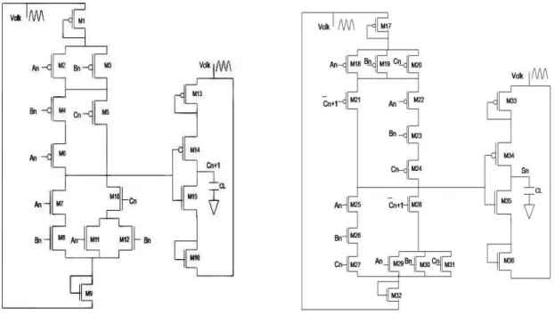
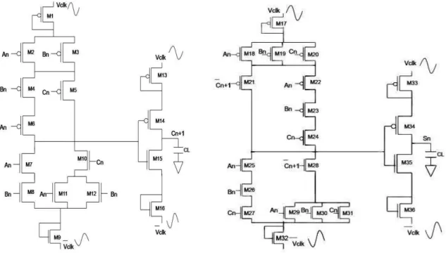
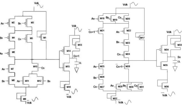
C. Design of Full Adder using 2Phase Drive Adiabatic Dynamic CMOS Logic
The schematics to realize the Carry and Sum functions of a full adder using 2PADCL are shown in figure. 10.
Figure 10. Schematics to implement Carry and Sum using 2PADCL.
ISSN : 0975-3397 Vol. 3 No. 9 september 2011 3214
Figure 11. Simulation Result of Full Adder using 2PADCL.
From the figure 11, we can see that, we are getting ripple free output and the delay problem associated with adcl logic has been eliminated to a good extent by 2padcl logic.
D. Design of Full Adder using Glitch Free and Cascadable Adiabatic Logic
The schematics to realize the Carry and Sum functions of a full adder using GFCAL are shown in figure 12.
Figure 12. Schematics to implement Carry and Sum using GFCAL.
ISSN : 0975-3397 Vol. 3 No. 9 september 2011 3215
Figure 13. Simulation Result of Full Adder using GFCAL.
As we observed in GFCAL inverter, GFCAL does have significant propagation delay as was the case in adcl logic due to the use of single power clock.
E. 2 Phase Clocked Adiabatic Static CMOS Logic
The schematics to realize the Carry and Sum functions of a full adder using 2PASCL are shown in figure 14.
Figure 14. Schematics to implement Carry and Sum using 2PASCL.
ISSN : 0975-3397 Vol. 3 No. 9 september 2011 3216
Figure 15. Simulation Result of Full Adder using 2PASCL.
From the figure 15, we can observe the presence of ripples in the output due to absence of rectifying diode in charging path.
V. COMPARISONOF FULLADDERS
In the previous section, we successfully simulated the full adders designed with different adiabatic logic families along with static CMOS but with fixed parameters like fixed load capacitance and fixed input frequency and fixed temperature. In real world, the full adder may need to operate under varying operating conditions or varying parameters. So we need to observe the effect of varying parameters or varying conditions on the full adder designed with different logic families and observe which design serves well in what condition. In this section, we have compared the full adders designed with different logic families on the basis of effect of variation of different parameters on the average power consumed by them and the propagation delay exhibit by them.
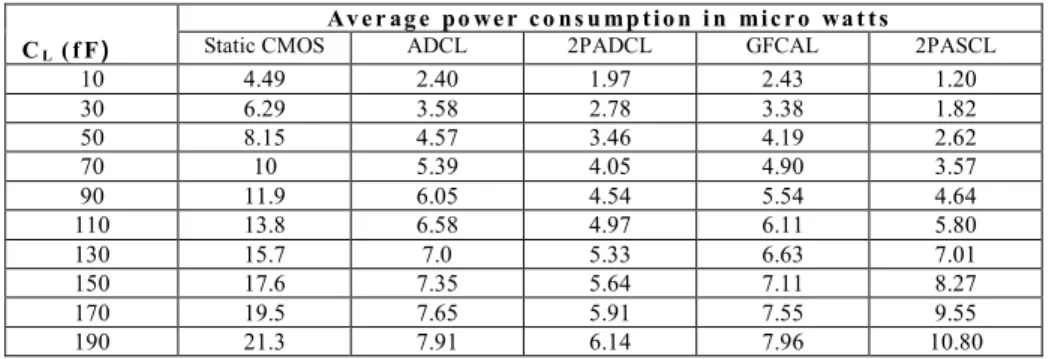
A. Effect of Variation in Load Capacitance on Average Power Consumption
In this section, we have observed the effect of variation in load capacitance on average power consumed by the full adders designed with different logic families. The results so obtained are compared together. We have kept power clock frequency to be 100MHZ. Input frequencies are 25MHZ, 12.5MHZ and 8.33MHZ respectively for input A, B and C of a full adder. The operating temperature is 25°C. The load capacitance CL is varied from 10 fF to 200 fF in steps of 20 fF and the resulting average power consumption is observed. The simulation results obtained are shown in Table I.
TABLE I. Variation of Average Power Consumption with Load Capacitance
CL (f F)
Av er ag e po wer co ns u mp tio n i n micro wa t ts
Static CMOS ADCL 2PADCL GFCAL 2PASCL
10 4.49 2.40 1.97 2.43 1.20
30 6.29 3.58 2.78 3.38 1.82
50 8.15 4.57 3.46 4.19 2.62
70 10 5.39 4.05 4.90 3.57
90 11.9 6.05 4.54 5.54 4.64
110 13.8 6.58 4.97 6.11 5.80
130 15.7 7.0 5.33 6.63 7.01
150 17.6 7.35 5.64 7.11 8.27
170 19.5 7.65 5.91 7.55 9.55
ISSN : 0975-3397 Vol. 3 No. 9 september 2011 3217 On the basis of simulation results shown in Table I, a graph has been plotted showing the variation of average power consumption with variation in Load Capacitance as shown in figure 16.
Figure 16. Variation of Average Power Consumption with Load Capacitance.
As we know, the dynamic power dissipation is dependent on load capacitance, the simulation results confirm it. The power dissipation is increasing in all the designs of full adder. From above graph, we found that, in the full adder designed with static CMOS logic, the average power consumption rises sharply with increment in load capacitance.
Under the simulation conditions mentioned, the full adder designed with ADCL tends to offer upto 63% power saving in comparison to full adder designed with static CMOS. The power saving is more pronounced at larger value of load capacitance than at smaller value of load capacitance. The full adder designed with 2PADCL tends to offer upto 71% power saving in comparison to full adder designed with static CMOS. Again, power saving is more pronounced at larger value of load capacitance. The full adder designed with GFCAL tends to offer upto 63% power saving in comparison to full adder designed with static CMOS. Like ADCL and 2PADCL, the power saving is more pronounced at larger value of load capacitance. The full adder designed with 2PASCL tends to offer upto 73% power saving in comparison to the full adder designed with static CMOS. But unlike ADCL, 2PADCL, GFCAL, the power saving in 2PASCL is more pronounced at smaller value of load capacitance. At the higher value of load capacitance, the power dissipation in 2PASCL rises sharply. The ability of a particular design of full adder to operate at larger load capacitance with smaller power dissipation enhances its fan out capability.
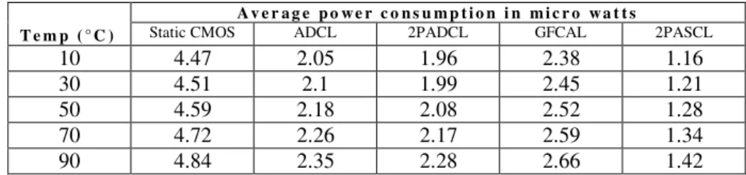
B. Effect of Variation in Temperature on Average Power Consumption
In this section, we have observed the effect of variation in operating temperature on average power consumed by full adders designed with different logic families. The results so obtained are discussed and compared together. We have kept power clock frequency to be 100MHZ. Input frequencies are 25MHZ, 12.5MHZ and 8.33MHZ respectively for input A, B and C of full adder. The load capacitance CL is fixed at 10f
farad and operating temperature is varied from 10°C to 90°C in the steps of 20°C.The resulting average power consumption is observed. The simulation results obtained are shown in Table II.
TABLE II. Variation of Average Power Consumption with Temperature
T e m p ( ° C )
A v e r a g e p o w e r c o n s u m p t i o n i n m i c r o w a t t s
Static CMOS ADCL 2PADCL GFCAL 2PASCL
10 4.47 2.05 1.96 2.38 1.16
30 4.51 2.1 1.99 2.45 1.21
50 4.59 2.18 2.08 2.52 1.28
70 4.72 2.26 2.17 2.59 1.34
ISSN : 0975-3397 Vol. 3 No. 9 september 2011 3218 On the basis of simulation results shown in Table II, a graph has been plotted showing the variation of average power consumption with variation in operating temperature as shown in figure. 17.
Figure 17. Variation of Average Power Consumption with Temperature.
The main component of power dissipation which is dependent on temperature is Static dissipation which arises due to –
(1) Leakage Current (2) Sub- threshold Current
Normally at nominal temperature this component of power dissipation is neglible, but both these currents tend to increase with increment in temperature and contribute a significant amount in overall power dissipation. We can easily see that the average power consumption is increasing with increment in temperature in almost every logic family. We also see that, the average power dissipation is increasing not by a large margin, as the static dissipation is not dominating factor in overall power dissipation. We can see from the above graph that the full adder designed with 2PASCL consumes minimum power for entire temperature range and offer upto 74% of power saving in comparison of full adder designed with static CMOS. As expected, the logic family, 2PADCL consumes less power than ADCL for entire temperature range and offer upto 56% power saving in comparison to full adder designed with static CMOS. The full adder designed with ADCL offer upto 54% power saving and the full adder designed with GFCAL offer upto 47% power saving in comparison to the full adder designed with static CMOS. The saving in power is more pronounced at low temperature in all the designs of full adder.
C. Effect of Variation in Input Frequency on Average Power Consumption
In this section, we have observed the effect of variation in input frequency on average power consumed by the full adders designed with different logic families. The results so obtained are compared together.
We have kept power clock frequency to be 100MHZ. The load capacitance CL is fixed at 10f farad and
operating temperature is kept at 25°C. Here to represent frequency, we have used TON. Now, as we have used
square pulse as input, we have TON = TOFF, so frequency, f =1/T, where T = TON + TOFF. So, as TON will
increase, the frequency will decrease. Also, as full adder has three inputs; A, B and C, we have selected their time periods as TA =2TB =3TC . Here we have shown the variation of average power consumption with TON of
ISSN : 0975-3397 Vol. 3 No. 9 september 2011 3219 TABLE III. Variation of Average Power Consumption with TON or Input Frequency
TA( O N )
A v e r a g e p o w e r c o n s u m p t i o n i n m i c r o w a t t s
Static CMOS ADCL 2PADCL GFCAL 2PASCL
50 9.40 4.46 4.21 3.50 4.74
100 4.51 2.26 2.25 2.41 1.82
150 3.06 1.99 1.63 1.93 1.51
200 2.26 1.45 1.24 1.66 1.03
250 1.79 1.19 0.97 1.45 1.15
300 1.49 0.98 0.82 1.33 0.56
350 1.38 0.94 0.77 1.24 0.93
400 1.14 0.76 0.63 1.10 0.61
450 1.05 0.72 0.58 1.07 0.61
500 0.90 0.57 0.57 1.06 0.5
On the basis of simulation results shown in Table III, a graph has been plotted showing the variation of average power consumption with variation in TON (A) as shown in figure 18.
Figure 18. Variation of Average Power Consumption with TON or Input Frequency.
Input frequency determines how often the logic switches between 1 and 0 and thus influences the power consumption of the gate. The variation of power consumed for various input data pulse widths is shown in figure. It is observed that lower input frequencies (higher time periods) give a low power dissipation. With increase in frequency the power dissipation is increased as the possibility of logic switching between 1 and 0 is increased. Hence at higher input frequency, almost every logic family tends to show increased power consumption. But we also see that some logic families show fluctuation in power dissipation/power consumed and that is expected. The power dissipation in adiabatic logic also depends on the value of power clock at the instant of switching. In adiabatic logic, the potential difference between the nodes through which charging or discharging will take place should be minimum at the time of switching. But as the input frequency is varied, the value of power clock at the time of switching may be different for different values of input frequency. This fluctuation is more pronounced in logic families which have ripples in the output. Because in these logic families, the potential difference between nodes can be different at the time of switching.
ISSN : 0975-3397 Vol. 3 No. 9 september 2011 3220 reason explained earlier in the text; presence of extra load capacitance in ADCL. The full adder designed with GFCAL offer upto 63% power saving in comparison to the full adder designed with static CMOS. But at some input frequencies, the GFCAL based design tends to consume maximum power and it may exceed the power consumed by static CMOS based design. Although, ADCL and GFCAL are very much similar in structure, they also show variation in power dissipation. Remember GFCAL is using triangular power clock which have different characteristic like rate of rise etc in comparison to sinusoidal clock used by ADCL. So at the instant of switching the value of power clock in GFCAL may be different from value of power clock in ADCL at different values of input frequency. As we know different value of power clock at the time of switching will give different power dissipation, the ADCL and GFCAL will show different power dissipation. The full adder designed with 2PASCL offer upto 62% power saving in comparison to the full adder designed with static CMOS. It is also observed that, in the 2PASCL based design, the power dissipation is fluctuating in nature: at some input frequencies it consumes very low power and at some frequencies it consumes more power. The reason for the fluctuation is already mentioned earlier.
D. Comparison of Propagation Delay
In the previous section, we compared the different designs of full adder on the basis of average power consumed by them for different values of parameters or operating conditions. As we know in adiabatic logic, the reduction in power dissipation comes at the expense of increased propagation delay or decreased operating speed and increased fabrication space. To know which design of full adder offers maximum operating speed and which design offers least operating speed, we have compared the propagation delay exhibit by them to compute the output –„Carry‟.
Here we have kept power clock frequency to be at 100 MHZ, CL at 10femto farad and input frequencies are kept at 25MHZ, 12.5MHZ and 8.33MHZ for three inputs of full adder.
The propagation delay exhibit by each full adder designed with different logic families to compute „Carry‟ is shown in Table IV.
TABLE IV. Comparison of Propagation Delay
Logic Family Average Propagation Delay
Static CMOS 0.1ns
ADCL 6.58ns
2PADCL 2.04ns
GFCAL 6.91ns
2PASCL 2.30ns
As we can see from Table IV, minimum propagation delay is offered by static CMOS based full adder. Maximum propagation delay is in GFCAL based adder, as it uses a single triangular clock as power supply. In this case delay is dependent on time period of power supply and here we are using a triangular power supply. So, delay is dependent on time period of this power supply. After that the full adder, which takes high propagation delay and is very close to GFCAL in terms of propagation delay is ADCL based full adder, which again uses a single power clock and delay is dependent of time period of this power supply. The adiabatic full adder, which has least propagation delay, is based on 2PADCL. We also verified that 2PASCL has least τphl. 2PASCL uses one extra diode to improve the discharging speed. So discharging occurs through that diode and NMOS and diode combination.
Remember that power and delay characteristics of any logic family also depend on timing of power clock with respect to input. So changing the timing of power clock, we can change the delay properties. For example, it can be verified by simulation that by changing the timing of power clocks in 2PASCL logic family, it shows very small delay, but at the expense of increased power consumption.
VI. CONCLUSION
ISSN : 0975-3397 Vol. 3 No. 9 september 2011 3221 require only one power clock and some require two power clocks. So, selection of a particular design of full adder is a difficult choice. Still, if the selection is to be made on the basis of high fan out capability, low propagation delay and low power consumption for most of the operating conditions, the full adder designed with 2PADCL can be a good choice. It has good speed of operation, high fan out capability and it dissipates low power for most of the conditions considered here. But it suffers from the drawback of floating node and it requires two power clocks.
REFERENCES
[1] G. Dickinson and J. S. Denker, “Adiabatic Dynamic Logic”, IEEE Journal of Solid – State Circuits, Vol. 30, No. 03, pp. 311 -315, March 1995.
[2] A. P. Chandrakasan and R. W. Brodersen, “ Low-power CMOS digital design”, Kluwer Academic Publishers, Boston,
1995.
[3] Yeap, “Practical low power digital VLSI design”, Kluwer academic publishers, 1998.
[4] J. M. Rabaey and M. Pedram, “Low Power Design Methodologies”, Kluwer Academic Publishers, Boston, 1996.
[5] K. Kaishita, M. Hashizume, H. Yotsuyanagi and T. Tamesada, “Low power dynamic CMOS logic circuits”, Shikoku – Section Joint convention Record of the Institute of Electrical and Related Engineers (Japanese Edition), pp. 138, October 2003.
[6] K. Roy and Y. Ye, “Energy recovery circuits using reversible and partially reversible logic”, IEEE Transactions on Circuits and Systems-I: Fundamental Theory and Applications, Vol .43, No. 09, pp. 769 – 778, September 1996
[7] K. Takahashi and M. Mizunuma, “Adiabatic dynamic CMOS logic circuits”, IEICE Trans. Electron., Vol. J81CII, Issue 10, pp. 810 -817, October 1998.
[8] M. Horowitz, T. Indennaur and R. Gonzalez, “Low Power Digital Design”, Technical Digest IEEE Symposium Low
Power Electronics, San Diego, pp. 08-11, October 1994.
[9] N. Anuar, Y. Takahashi, and T. Sekine, “Two phase clocked adiabatic static CMOS logic”, Proc. IEEE SOCC 2009, pp. 83-86, Oct. 2009.
[10] N. Anuar, Y. Takahashi, and T. Sekine, “Two phase clocked adiabatic static CMOS logic and its logic family,” Journal of Semiconductor Technology and Science, Vol. 10, No. 01, pp. 1-10, March 2010.
[11] N.S. S. Reddy, M. Satyam and K. L. Kishore, “Cascadable adiabatic logic circuits for low power applications”, IET Circuits Devices Syst., Vol. 2, No. 06, pp. 518 – 526, 2008.
[12] V. I. Starosel‟Skii, “Adiabatic logic circuits: A Review”, Russian Microelectronics, Vol. 31, No. 01, pp. 37-58, 2002.
[13] Y. Moon and D. K. Jeong, “An Efficient Charge Recovery Logic Circuit”, IEEE Journal of Solid State Circuits, Vol. 31, No. 04, pp. 514 -522, April 1996.