709 PACS numbers: 85.30.Tv, 85.30.Kk, 73.40.Ei
METAL-SEMICONDUCTOR FIELD-EFFECT TRANSISTORS
FABRICATED USING DVT GROWN n-MoSe2 CRYSTALS WITH
Cu-SCHOTTKY GATES
C.K. Sumesh1, K.D. Patel2, V.M. Pathak2, R.Srivastava2
1 Department of Physics, Charotar Institute of Technology, Charusat, Changa, 388 420, Anand, India
E-mail: [email protected]
2 Department of Physics, Sardar patel University, V.V. Nagar, 388 120, Anand, India
Metal-semiconductor field-effect transistors (MESFETs) based on DVT grown MoSe2 crystals and Cu Schottky gate have been fabricated and studied. When Schottky gate voltage (Vgs) changes from 0 to 10 V, the source-drain current (Ids) increases exponentially with Vgs and the conductance shows a drastic increase with positive Vgs. The fabricated n-MoSe2 MESFET have a saturated current level of about 100 mA and maximum transconductance of about 53 mA/V. Their results suggest a way of fabricating MESFETs from layered metal dichalcogenide semiconducting materials.
Keywords: MoSe2, MESFET, OHMIC CONTACT, SCHOTTKY CONTACT, I-V ANALYSIS.
(Received 04 February 2011)
1. INTRODUCTION
MoSe2 - molybdenum dichalcogenide has provided extra incentive to device research due to its layered structure. The intra-layer bonding of MoSe2 is predominantly covalent, while the interlayer bonding is of weak van der Waals type. Hence the crystals can be easily cleaved across the van der Waals gap. The resulting (001) basal plane contains a close-packed hexagonal array of chemically saturated chalcogenide ions. Thus, it does not contain dangling bonds with which adsorbates may react and hence can be considered to be free of surface states [1-3]. This chemical inertness of the basal plane of MoSe2 makes it ideal for the fabrication of Schottky barrier devices, FETs, solar cell, etc. [4-7].
There have been many reports on the electrical and photoelectrical properties for the hexagonal MoSe2 materials [1-15]. But, in contrast to other layered semiconductors, to our knowledge, no report could be found on devices like MESFETs and its analysis. In this wok, n-type MoSe2 MESFETs were fabricated and the electrical characteristics were analyzed using I-V method.
2. EXPERIMENTAL
MESFET structure. MoSe2 crystals with flat shining surfaces, chosen with the help of optical microscope, were washed in acetone to remove contaminations and to make the surface clean. The cleaned crystals were mounted on the substrate holder inside the vacuum chamber for fabricating Schottky contacts. Copper has been selected as the gate material as it shows very good rectification behaviour with MoSe2 [16]. Copper metal dots of area 2,62 ´ 10 –3 cm2 were deposited using thermal evaporation technique. In order to get evaporated thin metal film deposited in confined areas on the crystal surface, crystals were masked with a thin metal sheet having appropriate circular holes. After reaching a vacuum level of ~10 – 6 torr, pure copper metal (3 k樔) was evaporated from a W-helical boat onto the semiconductor surface. The rate of evaporation was kept very low i.e. 2 樔/sec in order to make the deposition uniform over the whole area. In addition, this gives good adhesion and other desirable properties in the fabricated Schottky diodes resulting basically from relatively slower growth mechanisms.
The front electrical contacts with evaporated copper regions were taken with low strain copper wires and Au paste (Eltec-1228C). The two ohmic contacts called source and drain (shown in figure1) were taken with indium metal ingot which was fused onto the same surface of MoSe2 along with low strain thin Ag alloy wires (Lakeshore wire part No.671-260) with the help of a fine tip soldering iron [16].
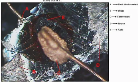
Fig. 1 – A typical optical micrograph (20X) of MoSe2 MESFET
The whole assembly was fixed on a mica piece for support and utmost care was taken during the whole process to keep the prepared structure intact because MoSe2 crystals are very much soft and brittle.
There are various methods for the determination of MESFET parameters. Amongst these current – voltage (I-V) analysis and capacitor –
3. RESLTS AND DISCUSSION
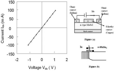
The current-voltage characteristics of a n-type MoSe2 layer in which electrons are carrying the current is important and has been shown in figure 2 as obtained between the source and drain. When a positive voltage Vds is applied to the drain, electrons will flow from source to drain. Hence
the source acts as the origin of carriers and the drain as a sink. As evident from figure 2, the semiconductor layer behaves like a linear resistor.
Fig. 2 – Drain –Source I-V characteristics of n-type MoSe2 MESFET. Inset figures (a) show the contacts to the n-type MoSe2 channel and (b )tunnelling of electrons across the In-nMoSe2 Ohmic interface
The gate contact in a MESFET device should be a Schottky barrier. Proper rectification of diode junctions within a MESFET structure is necessary for its electrical operation [17]. Figure 3 shows the I-V characteristics of the metal semiconductor Schottky junction formed by the Cu metal gate on the n-type MoSe2 channel. It shows excellent rectification behavior, which indicates a good Schottky contact between copper and n-type MoSe2 crystal. The inset figure shows the energy band diagram of n-type MoSe2 and Cu. The high work function Cu metal forms a potential barrier for electrons.
-2.5 -1.5 -0.5 0.5 1.5 2.5
Voltage Vgd ( V )
C
u
r
re
n
t I
g
d
(
m
A
)
0 60
30 90
-90 -60 -30
Fig. 3 – I-V characteristics of the metal semiconductor Schottky junction formed by the copper gate on the n-type MoSe2 channel. The inset figure is energy band diagram of n-type MoSe2 and Cu
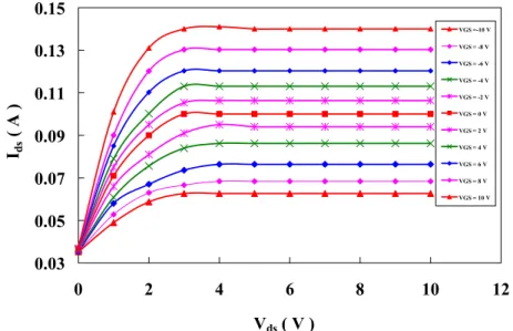
In Fig. 4 the source-drain current (Ids) is plotted as a function of applied drain source voltage (Vds) for several different gate-source voltages (Vgs). The
source electrode was grounded. We can see that the Ids increases with Vds for
a given Vgs, and the conductance shows a drastic increase with positive Vgs.
The device transconductance is defined as the slope of the Ids-Vgs
characteristics with the drain-source voltage held constant according to Eq. 1.
0.03 0.05 0.07 0.09 0.11 0.13 0.15
0 2 4 6 8 10 12
Vds ( V )
Ids
(
A
)
VGS =-10 V VGS = -8 V VGS = -6 V VGS = -4 V VGS = -2 V VGS = 0 V VGS = 2 V VGS = 4 V VGS = 6 V VGS = 8 V VGS = 10 V
Fig. 4 – Drain current as a function of drain-source voltage for different gate bias in the range ± 10 V for n – MoSe
=
=
constant ds ds m
gs V
dI g
dV (1)
The maximum transconductance of about 53 mA/V and has been obtained at constant Ids = 10 V. The saturated current level (saturated
current level - Idss is the drain source current at Vgs = 0) of the device was
found to be Idss= 100 mA. Thus it is seen that DVT grown n-MoSe2 crystals show a good potential for flexible MESFET device development as basal plane layers of this crystals can behave as good conducting channel and copper contacts to it offers a good Schottky gate contact.
4. CONCLUSION
We have fabricated n-MoSe2 MESFET based on DVT grown MoSe2 crystals. A top copper Schottky contact was used as gate and indium ohmic contacts were used as source and drain. The MESFET’s electrical behavior follows the established MESFET theory. The fabricated n-MoSe2 MESFET have a saturated current level of about 100 mA and maximum transconductance of about 53 mA/V.
Financial support received in the form of UGC major research project (Grant reference No.:F33-8/2007(SR) by Dr. K.D.Patel is thankfully acknowledged
REFERENCES
1. J. Pouzet, J.C. Bernede, Mater. Chem. Phys.36, 304 (1994). 2. J.M. Huang, D.F. Kelley, Chem. Mater.12, 2825 (2000).
3. R. Harpeness, A. Gedanken, A.M. Weissb, M.A. Slifkin, J. Mater. Chem. 13, 2603 (2003).
4. S.R. Cohen, L. Rapoport, E.A. Ponomarev, H. Cohen, T. Tsirlina, R. Tenne, C. Levy-Clement, Thin Solid Films324, 190 (1998).
5. A. Hussain, S. Auluck, Phys. Rev. B71, 155114 (2005).
6. Th. Boker, R. Severin, A. Muller, C. Janowitz, R. Manzke, Phys. Rev. B 64, 235305 (2001).
7. S. Sugai, T. Ueda, Phys.Rev. B 26, 6554 (1990).
8. C.K. Sumesh, K.D. Patel, V.M. Pathak, R. Srivastava, Journal of Ovonic Research4, 61 (2008).
9. C.K. Sumesh, K.D. Patel, V.M. Pathak, R. Srivastava, Chalcogenide Lett.5, 177 (2008).
10.S.Y. Hu, C.H. Liang, K.K. Tiong, Y.S. Huang, J. Alloy. Compd.442, 249 (2007). 11.Y.C. Lee, G.W. Shu, W.Y. Uen, J.L. Shen, W.Y. Uen, Solid. State Commun.
123, 421 (2002).
12.M.K. Agarwal, P.D. Patel, S.K. Gupta, J. Cryst. Growth.129, 559 (1993). 13.V.M. Pathak, K.D. Patel, R.J. Pathak, R. Srivatava, Solar Energ. Mat. Sol. C.
73, 117 (2002).
14.M.K. Agarwal, P.D. Patel, O. Vijayan, Phys. Status Solidi A78 133 (1983). 15.B.L. Evans and R.A. Hazelwood, Phys. Status Solidi A4, 181 (1971).
16.C.K. Sumesh, K.D. Patel, V.M. Pathak, R. Srivastava, Cryst. Res. Technol. 46, 61 (2011).