J. Nano- Electron. Phys.
3 (2011) No1, P. 610-619 (Sumy State University) 2011 SumDU
610 PACS numbers: 68.37.Hk, 75.40.Cx
MAGNETIC AND ELECTRIC PROPERTIES OF SEMICONDUTER
BISMUTH TRI SULPHIDE (BI2S3) GROWN BY GEL METHOD
T.K. Patil1, K.B. Saraf2
1 Smt. G.G. Khadse Science,
Arts and Com. College, Muktainagar – 425 306, India 2 Pratap College, Amalner – 425 401, India
E-mail: [email protected]
In the present investigation, crystals of bismuth Tri Sulphide (Bi2S3) were grown by a simple gel technique using single diffusion method. The optimum growth conditions were established by varying various parameters such as pH of gel solution, gel concentration, gel setting time, concentration of reactant etc. Gel was prepared by mixing sodium meta silicate (Na2SiO35H2O), glacial acetic acid (CH3COOH) and supernant bismuth chloride (BiCl3) at pH value 4.4 and transferred in glass tube of diameter 2.5 cm and 25 cm in length. The mouth of test tube was covered by cotton plug and kept it for the setting. After setting the gel, it was left for aging. After 13 days duration the second supernant H2S water gas solution was poured over the set gel by using pipette then it was kept undisturbed. After 72 hours of pouring the second supernatant, the small nucleation growth was observed at below the interface of gel. The good quality Orthorhombic or Rhombus Bi2S3 crystals were grown in 31 days. These grown crystals were characterized by Magnetic Susceptibility, Electrical Conductivity, EDAX and SEM.
Keywords: GEL GROWN BI2S3 CRYSTALS, MAGNETIC SUSCEPTIBILITY,
ELECTRICAL CONDUCTIVITY, EDAX AND SEM. (Received 04 February 2011)
1. INTRODUCTION
MAGNETIC AND ELECTRIC PROPERTIES OF SEMICONDUTER… 611
present study, crystals of Bi2S3 were grown by a simple gel technique using single diffusion method. The optimum growth conditions for crystals were obtained. These conditions were established & reported.
2. MATERIALS AND METHODS
Test tubes are used as crystallizing vessels. Sodium met silicate (Na2SiO35H2O) gel was used as a growth media. Gel was prepared by glacial acetic acid and sodium metal silicate, having different pH values .The chemical used for growth of single crystals of Bismuth Tri-Sulphide were CH3COOH, Na2Sio35H2o, Bicl3 or Bi(No3)3 and H2S water gas solution all chemicals are of AR grade .Different molar masses were tried to determined the optimum growth conditions one of the reactant having different concentration were incorporated into gel. This solution was then transferred into borosil glass tube of diameter 2.5 cm and 25 cm in length (height). The mouth of the tube was covered by cotton plug. After setting of the gel it was left for aging for different periods of time other reactant having different concentrations was then added as supernant over the set gel. Experiments were carried out by changing different concentration of the reactants. The Chemical reaction inside the gel can be expressed as,
XCl3 + 3Y2S → X2S3 + 6YCl Or
2X(NO3)3 + 3Y2S → X2S3 + 6Y(NO)3 Where X Bi and Y K or Na
3. RESULT AND DISCUSSION
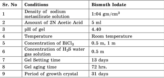
The optimum conditions for growth of bismuth Tri Sulphide crystals’ are as shown in Table 1 and effect of concentration of reactant on habit and size of Bismuth Tri Sulphide crystals are given in Table 2.
Table 1 – Optimum conditions for growth of bismuth Tri Sulphide crystals
Sr. No Conditions Bismuth Iodate
1 Density of sodium metasilicate solution 1:04 gm/cm3 2 Amount of 2N Acetic Acid 5 ml
3 pH of gel 4.40
4 Temperature Room temperature
5 Concentration of BiCl3 0.5 m, 1 m 6 Concentration of H2S water
gas solution 0.5 m
7 Gel Setting time 13 days
8 Gel aging time 72 hrs.
612 T.K. PATIL, K.B. SARAF
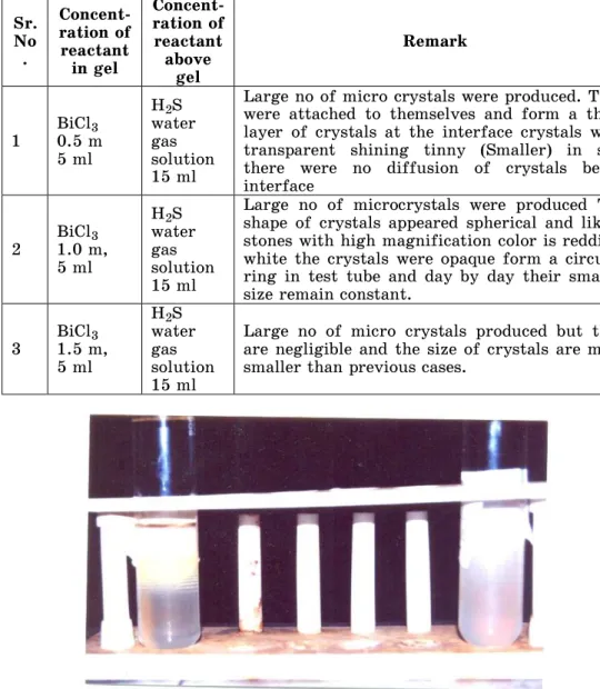
Table 2 – Effect of concentration of reactant on habit and size of Bismuth Tri Sulphide crystals
Sr. No
.
Concent-ration of reactant in gel
Concent-ration of
reactant above
gel
Remark
1 BiCl0.5 m 3 5 ml
H2S water gas solution 15 ml
Large no of micro crystals were produced. They were attached to themselves and form a thick layer of crystals at the interface crystals were transparent shining tinny (Smaller) in size there were no diffusion of crystals below interface
2 BiCl1.0 m, 3 5 ml
H2S water gas solution 15 ml
Large no of microcrystals were produced The shape of crystals appeared spherical and like a stones with high magnification color is reddish, white the crystals were opaque form a circular ring in test tube and day by day their smaller size remain constant.
3 BiCl1.5 m, 3 5 ml
H2S water gas solution 15 ml
Large no of micro crystals produced but they are negligible and the size of crystals are more smaller than previous cases.
MAGNETIC AND ELECTRIC PROPERTIES OF SEMICONDUTER… 613
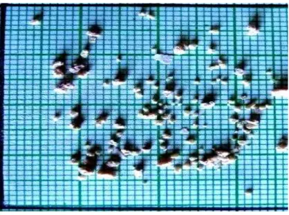
Fig. 2 – Few crystals of Bismuth Tri Sulphide
Fig. 1. Shows transparent crystals of Bismuth Tri Sulphide attached to themselves and forming a thick layer at the interface Fig. 2. Shows different habits with their scaling on a graph paper .Grown Bismuth Tri Sulphide crystals were characterized by Magnetic Susceptibility, Electrical Conductivity, and EDAX and SEM.
3.1 Magnetic Susceptibility
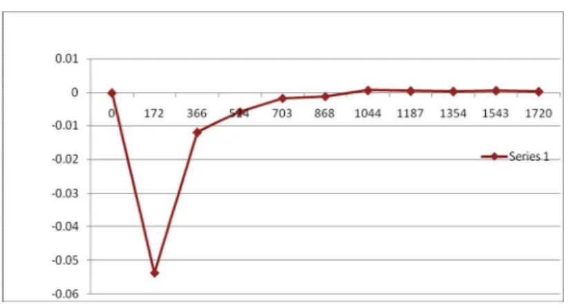
Experiment for Bismuth Tri Sulphide Table 3 – Magnetic Susceptibility of Bi2S3
Sr.No Current in A
Magnetic Field (H) Guass
Weight of sample in
gm
Difference
in wt m m 10
– 6 cm3 mole – 1
1 0 0 4.615 ---- 0
2 0.2 172 4.617 - 0.002 - 0.05385
3 0.4 366 4.617 - 0.002 - 0.01189
4 0.6 524 4.617 - 0.002 - 0.005802
5 0.8 703 4.616 - 0.001 - 0.001611
6 1.0 868 4.616 - 0.001 - 0.001057
7 1.2 1044 4.614 + 0.001 + 0.0007309
8 1.4 1187 4.614 + 0.001 0.0005654
9 1.6 1354 4.614 + 0.001 0.0004345
10 1.8 1543 4.613 + 0.002 0.0006692
11 2.0 1720 4.613 + 0.002 0.0003885
Observations:
614 T.K. PATIL, K.B. SARAF
b) Weight of empty holder + Holder Assembly (test tube) + sample powder without magnetic field 4.615 gm
c) Weight of sample powder M b – a 4.615 – 4.595 0.020 gm
m Change in weight (m) of sample powder with magnetic field 0.002 gm
L Height of sample powder in test tube 1.1 cm Density of specimen 7.39 g/cm3
H Applied magnetic field 366 gauss (for 0.4 A current) M Weight of specimen examine 0.020 gm
g Acceleration due to gravity 980 cm/sec2
Formula: The magnetic succeptibility () of Bismuth Tri Sulphide (Bi2S3) powder is given by relation. 2mgL / MH2 2 980 1.1 7.39 (– 0.002) / 0.020 (366)2 – 0.01189
Fig. 3 – Graph of Magnetic Field (H) Guass V/s m 10 – 6cm3mole – 1
3.2 Electrical Conductivity Of Bismuth Tri Sulphide Bi2S3 OBSERVATIONS: 1) Height / thickness of pallet 0.536 cm OBSERVATIONS: 2) Diameter of the pallet 0.942 cm OBSERVATIONS: 3) Radius of pallet r 0.471 cm d/2 OBSERVATIONS: 4) Voltage 0.50 mv (constant)
K l/RAK l/Rr2 (since A r2 ) l 0.536 cm 5.36 10 – 4 m r 0.471 cm 4.71 10 – 4 m)
K 5.36 10 – 4 / R 3.142 (4.71 10 – 4)2 K 5.36 10 – 4 / R 3.142 (4.71)2 10 – 8 K 5.36 / R 3.142 (4.71)2 10 – 4
MAGNETIC AND ELECTRIC PROPERTIES OF SEMICONDUTER… 615
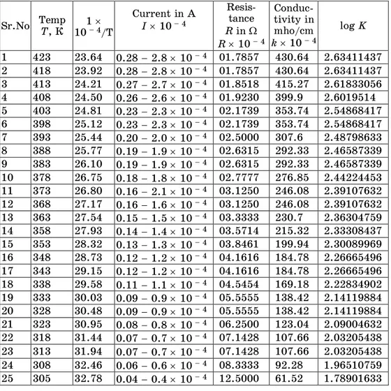
Table 4 – Electrical Conductivity Of Bismuth Tri Sulphide Bi2S3
Sr.No Temp T, К 1 10 – 4/T
Current in A I 10 – 4
Resis-tance R in R 10 – 4
Conduc-tivity in mho/cm k 10 – 4
log K
1 423 23.64 0.28 2.8 10 – 4 01.7857 430.64 2.63411437 2 418 23.92 0.28 2.8 10 – 4 01.7857 430.64 2.63411437 3 413 24.21 0.27 2.7 10 – 4 01.8518 415.27 2.61833056 4 408 24.50 0.26 2.6 10 – 4 01.9230 399.9 2.6019514 5 403 24.81 0.23 2.3 10 – 4 02.1739 353.74 2.54868417 6 398 25.12 0.23 2.3 10 – 4 02.1739 353.74 2.54868417 7 393 25.44 0.20 2.0 10 – 4 02.5000 307.6 2.48798633 8 388 25.77 0.19 1.9 10 – 4 02.6315 292.33 2.46587339 9 383 26.10 0.19 1.9 10 – 4 02.6315 292.33 2.46587339 10 378 26.75 0.18 1.8 10 – 4 02.7777 276.85 2.44224453 11 373 26.80 0.16 2.1 10 – 4 03.1250 246.08 2.39107632 12 368 27.17 0.16 1.6 10 – 4 03.1250 246.08 2.39107632 13 363 27.54 0.15 1.5 10 – 4 03.3333 230.7 2.36304759 14 358 27.93 0.14 1.4 10 – 4 03.5714 215.32 2.33308437 15 353 28.32 0.13 1.3 10 – 4 03.8461 199.94 2.30089969 16 348 28.73 0.12 1.2 10 – 4 04.1616 184.78 2.26665496 17 343 29.15 0.12 1.2 10 – 4 04.1616 184.78 2.26665496 18 338 29.58 0.11 1.1 10 – 4 04.5454 169.18 2.22834902 19 333 30.03 0.09 0.9 10 – 4 05.5555 138.42 2.14119884 20 328 30.48 0.09 0.9 10 – 4 05.5555 138.42 2.14119884 21 323 30.95 0.08 0.8 10 – 4 06.2500 123.04 2.09004632 22 318 31.44 0.07 0.7 10 – 4 07.1428 107.66 2.03205438 23 313 31.94 0.07 0.7 10 – 4 07.1428 107.66 2.03205438 24 308 32.46 0.06 0.6 10 – 4 08.3333 92.28 1.96510759 25 305 32.78 0.04 0.4 10 – 4 12.5000 61.52 1.78901633
Calculations : 1) I 0.28 m A 2.8 10 – 4 A V 0.5 mV 5 10 – 4 V
R V/I 5 10 – 4 / 2.8 10 – 4 1.7857 K 769.01 / R 769.01/1.7857
K 4.3064 100 K 430.64 mho/cm
1) I 0.27 m A 2.7 10-4 A V 0.5 mV 5 10 – 4 V
R V/I 5 10 – 4 / 2.7 10-4 1.8518 K 769.01 / R 769.01 / 1.8518
616 T.K. PATIL, K.B. SARAF
Fig. 4 – Graph of Temp T o k V/s log K
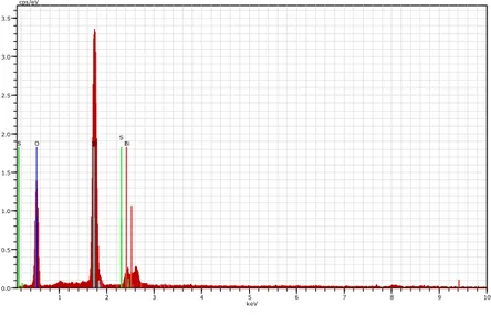
3.3 EDAX
Elemental Dispersive Analysis by X rays (E-DAX). Elemental analysis by X ray (EDAX) is used for the quantitative analysis. In the present work elemental analysis of gel grown Bismuth Tri Sulphide, crystals was carried out at the NCL National Chemical Laboratory Pune. Fig. 5 shows EDAX spectrum of Bismuth Tri Sulphide. Table 5 shows the values of elemental content of the crystals as measured by the EDAX technique and the theoretical calculations from molecular formula. From the table it is clear that values of (wt %) and (At %) of Bi2S3 in grown crystals measured EDAX are close to with the estimated values calculated from molecular formula.
1 2 3 4 5 6 7 8 9 10
keV 0.0
0.5 1.0 1.5 2.0 2.5 3.0 3.5
cps/eV
Bi O Si S S
MAGNETIC AND ELECTRIC PROPERTIES OF SEMICONDUTER… 617
Table 5 – For calculation of elemental analysis of gel grown Bismuth Tri Sulphide
Element Content measured by EDAX Content as calculated from molecular formula Bi 2S3
Wt % At % Wt % At %
Bismuth 76.07 % 67.48 81.28 % 74.76 Sulphur 15.26 % 20.57 18.70 % 21.68
Total 91.33% - 99.98 % -
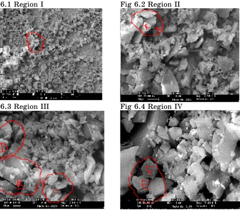
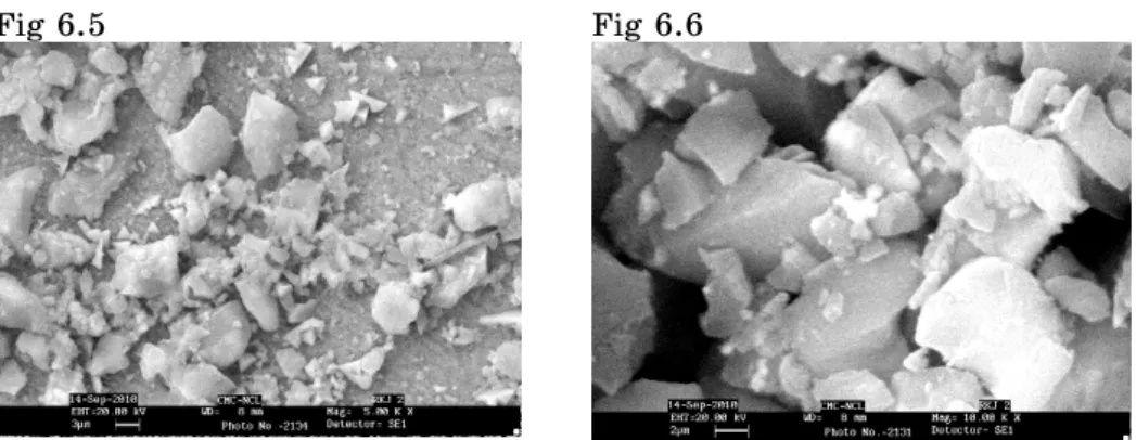
3.4 SEM
In present work Scanning Electron Microscopy of powdered sample of gel grown Bismuth Tri Sulphide crystals was carried at NCL (National Chemical Laboratory) Pune and the successive photographs were taken at the magnification of 0.5, 1.50, 2.00, 5.00 and 10.00 KX all the photographs were taken at common width 9 mm and EHT magnification 20 KV. And represented as Fig. 6.1 to 6.6 shows SEM images of the powdered sample of Bismuth Tri Sulphide. Fig. 6.1 shows the part of crystals of Bismuth Tri Sulphide. It is observed that the face is neither dull nor very bright but it has some bright region at the left half of the fig. whole the surface is covered with figs of different shapes and size. Some of the figs are approximately seen to be triangular and pentagonal.
Fig 6.1 Region I Fig 6.2 Region II
618 T.K. PATIL, K.B. SARAF
Fig 6.5 Fig 6.6
The edges triangle and pentagonal are clearly seen in some cases but in some cases they are not so cleared. In general the shape is clearly seen, these figs are randomly oriented on the whole surface.
In Fig. 6.1 a small region labeled as small (a) at 0.5 KX is shown as (A). In Fig. 6.2 at 1.50 KX the magnification all three Figures in A region are pentagonal on minute observation Figure (X) in region (A) is perfectly pentagonal with well defined boundaries while the remaining two figs does nit have well defined start boundaries. In Fig. 6.3 shows different region with higher magnification the edges of figs have in general marked boundaries because of higher magnification attachment of micro crystals are individual grains is clearly seen. The region marked by (B) in Fig. 6.3 shows attachment of many micro crystals. If we compare region (B), (C) and (D) on Fig. 3 region B has more attachment of micro crystals than region (C), also by comparing region (C) and (D) region (C) has maximum micro crystals than (D) means we compare the attachment of micro crystals in region (B), (C) and (D) simultaneously we may conclude that it is die to different growth conditions on the same face. The growth rate in the region (B) is higher as compare to region (C) and the growth rate is controlled in the region (D). This supports the fact that the growth conditions are varying on different parts of same face of the crystals. The same thing of growth conditions are observed in region (E) of Fig. 6.4. In region (E) one defined hexagon marked by (F) is seen to be in regular shape of hexagon having marked boundary and size of equal length ie from Fig. 6.4 shows controlled growth condition as attachment of micro crystals in different part of fig is less. Where as attachment of micro crystals is more in different part of Fig. 6.5 i.e. Region shown in Fig. 6.4 have controlled condition as compare to Fig. 6.5. If Fig. 6.6 is observed it indicates well defined some pentagon with no attachment of micro crystals i.e. it confrms the controlled growth conditions.
4. CONCLUSIONS
From the above studies, we observe that:
MAGNETIC AND ELECTRIC PROPERTIES OF SEMICONDUTER… 619
substance above 1 K Gauss. Magnetic susceptibility is decreased as increase in temperature.
II. The electrical conductivity of semiconductor crystals closely related to theoretical values with chemical nature of compound the electrical conductivity increases as increase in temperature
III. Gel growth technique is suitable for growing crystals of Bismuth Tri Sulphide.
IV. Different habits of Bismuth Tri Sulphide crystals can be obtained by changing parameters like gel density, gel aging, pH of gel, Concentration of reactants etc.
V. Crystals are quite transparent, and are of good quality.
VI. From EDAX the observed values well match with values calculated from molecular formula.
VII.From SEM the grain size of sample is pentagonal and traingular.
The authors are grateful to Prof. Dr. L.A. Patil, Head Department of Physics, Pratap College, Amalner, for providing laboratory facilities. Our special thanks to Department of Physical sciences, NMU, Jalgaon for providing Magnetic susceptibility and electrical conductivity facilities and authorities of NCL, Pune for EDAX and SEM facilities.
REFERENCES
1. S.L. Garud, K.B. Saraf, B. Mater. Sci.31, 639 (2008). 2. S.L. Garud, K.B. Saraf, B. Mater. Sc.32, 187 (2009). 3. Z. Blank, J. Cryst. Growth18, 281 (1973).
4. H. Bach, H. Kuppers, Acta Crystall. B-Stru.34, 263 (1978).
5. M. Schieber, A. Gril, I. Shidlovsky, J. Cryst. Growth3-4, 467 (1968). 6. K. Sangwal, A.R. Patel, J. Cryst. Growth23, 282 (1974).
7. M.S. Joshi, S.G. Trivedi, Indian J. Pure Ap. Phy. 21, 435 (1983). 8. Z. Blank, W. Brenner, Y. Okamoto, Mater. Res. Bull. 3, 555 (1968). 9. S.K. Kurtz, T.T. Perry, J Appl. Phys.39, 3798 (1968).
10.B. Morosin, J.G. Bergman, G.R. Crane, Acta Crystall. B-Stru.29, 1067 (1973). 11.Z. Blank, W. Brenner, Nature222, 79 (1969).
12.A.R. Patel, A.V. Rao, J. Cryst. Growth43, 351 (1978).
13.K. Nakamoto, Infrared spectra of inorganic and coordination compounds (New York: John Wiley and sons Inc.: 1970).
14.S.J. Shitole, K.B. Saraf, B. Mater. Sci.24, 461 (2001).
15.D. Ranadive, Z. Blank, W. Brenner, Y. Okamoto, Nature223, 829 (1969). 16.X.S. Shajan, C. Mahadevan, B. Mater. Sci.27, 327 (2004).
17.B.S. Kumar, M.H.R. Kutty, M.R.S. Kumar, K.R. Babu, B. Mater. Sci. 30, 349
(2007).
18.S.K. Arora, A.J. Kothari, R.G. Patel, K.M. Chauhan, B.N. Chudasama, J. Phys. Conf. Ser. 28, 48 (2006).