Stepped light-induced transient measurements of photocurrent and voltage
in dye-sensitized solar cells based on ZnO and ZnO:Ga
Agnaldo de Souza Gonçalves, Marian R. Davolos, Naruhiko Masaki, Shozo Yanagida, Shogo Mori et al.
Citation: J. Appl. Phys. 106, 064316 (2009); doi: 10.1063/1.3226073
View online: http://dx.doi.org/10.1063/1.3226073
View Table of Contents: http://jap.aip.org/resource/1/JAPIAU/v106/i6
Published by the AIP Publishing LLC.
Additional information on J. Appl. Phys.
Journal Homepage: http://jap.aip.org/
Journal Information: http://jap.aip.org/about/about_the_journal
Top downloads: http://jap.aip.org/features/most_downloaded
Stepped light-induced transient measurements of photocurrent and voltage
in dye-sensitized solar cells based on ZnO and ZnO:Ga
Agnaldo de Souza Gonçalves,1,4 Marian R. Davolos,1,a兲 Naruhiko Masaki,2 Shozo Yanagida,2Shogo Mori,3and Ana F. Nogueira4,b兲
1
Institute of Chemistry, Universidade Estadual Paulista (UNESP), Araraquara, São Paulo 14800-900, Brazil
2
Center for Advanced Science and Innovation, Osaka University, Suita, Osaka 565-0871, Japan
3
Department of Fine Materials Engineering, Shinshu University, Ueda 386-8567, Japan
4
Institute of Chemistry, Universidade Estadual de Campinas (UNICAMP), Campinas, São Paulo 13083970, Brazil
共Received 27 June 2009; accepted 19 August 2009; published online 29 September 2009兲
In order to explain the higher short-circuit current共Jsc兲with comparable open-circuit voltage共Voc兲
from dye-sensitized solar cells共DSCs兲based on gallium-modified ZnO共ZnO:Ga兲porous electrodes, the diffusion coefficient共D兲and electron lifetime共兲in DSCs with and without Ga-modified ZnO were studied by stepped light-induced transient measurements of photocurrent and voltage. In
comparison to DSCs based on ZnO electrodes, the ZnO:Ga-based solar cells provided lowerDand
higher values. The results were interpreted according to the transport-limited recombination
model, where the Ga modification induced a higher density of intraband charge traps. At matched
electron densities, a decrease in Voc from DSCs based on ZnO:Ga was observed, suggesting a
positive shift of the ZnO:Ga conduction band edge. The higherJsccan be explained by the positive
shift of the ZnO:Ga conduction band edge in addition to the increased roughness factor of the electrode due to the Ga modification. ©2009 American Institute of Physics.
关doi:10.1063/1.3226073兴
I. INTRODUCTION
Dye-sensitized solar cells共DSCs兲 have received signifi-cant attention in recent decades due to their respectable effi-ciency and low cost.1,2 The solar cells consist of a dye-adsorbed nanoporous semiconductor electrode immersed in an electrolyte and a Pt counterelectrode. One of the key is-sues to increase the energy conversion efficiency is to en-hance the electron transport in order to overcome the recom-bination losses inherent with the nanocrystalline film. Since the porous electrode is filled with an electrolyte, the electron transport has been described as a diffusion process due to the presence of cations, which screen the electrons in the electrode.3–5 The effect of cations on the electron transport has been interpreted in terms of ambipolar diffusion.6 Elec-tron diffusion in the nanostructured electrodes of DSCs has been described by a model that takes into account events of trapping by and detrapping from localized trap sites.5,7It has been shown that the traps are located mainly on the nanopar-ticle surface,8 and at interparticle boundaries.9 Since charge recombination in DSCs occurs through charge transfer at electrode/dye/electrolyte interface, charge recombination can be retarded by the proper surface modification of the semi-conductor oxide10or even by doping.11The use of Al and W
as photovoltaic property-enhancing impurities in TiO2 may
cause two effects: a different morphology 共and as a
conse-quence a different surface polarity兲, and a change in the de-fect content 共which affects the charge-transfer kinetics and dye loading兲.11 Solar cells based on doped TiO2 electrodes
presented a better performance in comparison to pristine TiO2counterpart, evidencing the role of surface polarity and
defect charge balancing on surface states.11An improvement in the incident photon to current conversion efficiency and overall conversion efficiency has also been reported for a DSC based on nitrogen-doped titania.12
ZnO has emerged as a versatile material for electrodes in DSCs especially due to facile modification of its
morphol-ogy, such as different nanostructures:13
nanorods/nanowires,14–16 nanoflowers,17 nanotubes18,19 and nanotips in addition to gallium-doped zinc oxide共ZnO:Ga or GZO兲as the transparent conductor oxide material,20etc. The
n-type semiconductor features of ZnO stem from the
pres-ence of intrinsic defects, such as oxygen/zinc vacancies, oxygen/zinc interstitials, and complex defects associated with oxygen/zinc vacancies.21 In order to enhance the elec-tron transport properties in ZnO nanostructured electrode, Ga3+was used in this work as the impurity ions, as surface
modifiers, and/or as dopants. In gallium-modified zinc oxide
共ZnO:Ga兲, Ga3+is expected to cause a little lattice distortion
due to the similar Zn2+ and Ga3+ tetrahedral radii.22 Ga im-purities act as a kind of donor in ZnO,23thereby affecting the point defect density and surface charge, a behavior probably
arising from the different Zn2+ and Ga3+ ionic charges.
Charge balance in ZnO:Ga 共Ref. 24兲 might require a
com-plex equilibrium between oxygen/zinc vacancies and
oxygen/zinc interstitials, while the formation of single oxy-gen vacancies is likely to take place. Since some native de-fects, e.g., single oxygen vacancies and zinc interstitials, have energy levels close to the ZnO conduction band edge,13 the electron density in ZnO would increase up to a certain
a兲
FAX: 55 16 33016692. Tel.: 55 16 3301 6634.
b兲Electronic mail: [email protected].
gallium doping level.25 The higher electron density arising
from Ga doping21 produces many-body effects resulting in
the renormalization of the band gap, lowering the band gap
energy.21 However, the role of Ga doping into ZnO still
needs further studies,21 especially if the formation of other crystalline phases, such as zinc gallate,22,26takes place. Even though there are many reports on the electron diffusion co-efficient共D兲and electron lifetime共兲for electrodes based on TiO2, little is known about ZnO electrodes. Recently we
re-ported the enhancement of the photocurrent and overall effi-ciencies in DSCs based on GZO porous electrodes compared
to ZnO.27 The aim of this work is to elucidate the higher
energy conversion efficiencies of DSCs based on ZnO:Ga by means of stepped light-induced transient measurements of photocurrent and voltage共SLIM-PCV兲.
II. EXPERIMENTAL SECTION
ZnO and ZnO:Ga 1, 3, and 5 at% nanoparticles were
prepared in an aqueous solution of zinc nitrate and/or gal-lium nitrate in the presence of triethanolamine.28 The paste
was spread onto the conducting substrate 共fluorine-doped
SnO2, Hartford Glass Co. 8 – 12 ⍀/䊐兲by the doctor blading
technique and then sintered at 450 ° C for 30 min. The elec-trodes were sensitized in a 0.5 mmol L−1 ethanolic solution
of the complex N719 关cis-bis共isothiocyanato兲bis共2,
2
⬘
-bipyridyl-4, 4⬘
-dicarboxylate-ruthenium共II兲bis-tetrabutylammonium兴for 3 h at room temperature. The
elec-trolyte was 0.5 mol L−1 4-tert-butylpyridine, 0.8 mol L−1
tetrabutylammonium iodide, 0.1 mol L−1 LiI, and
0.05 mol L−1 I
2 in methoxypropionitrile:acetonitrile 共50:50
v/v兲. The counterelectrode was a Pt-sputtered conducting
substrate. The DSCs were sealed by using the thermoplastic Himilan共Mitsui-Dupont Polychemicals兲. Film thickness was
⬃6 m共measured by the Sloan Technology profiler, Dektak
3兲and typical cell area was 0.15 cm2. For SLIM-PCV
mea-surements, a diode laser 共Coherent, LabLaser, = 635 nm兲
was used for both photocurrent and voltage transients, as
described elsewhere.29 Since D and exhibit some
depen-dence on dye loading, the amount of dye adsorbed into the
porous nanostructured electrodes was measured.30 The dye
was desorbed from the porous films by using a 1 mol L−1
NaOH solution 共water:ethanol 1:1 v/v兲, and the dye loading was determined from the absorption spectra of the solution.
The J-V curves of the sealed DSCs were measured under
AM 1.5 illumination共100 mW cm−2兲using a solar simulator
共Yamashita Denso, YSS-80兲. The data for J-V curves and
SLIM-PCV measurements were the average for at least three identical samples.
III. RESULTS AND DISCUSSION
The porosity of the porous nanocrystalline electrodes in-creased upon increasing the gallium content, as reported by
our group in an earlier paper.27 The increase in roughness
factor, that is, a higher actual area per projected area ratio, provided a higher dye loading upon increasing gallium con-tent, which is reflected in a higher short-circuit photocurrent density共Jsc兲, as observed in TableI. However, the increase in
roughness factor is not enough to explain the increase inJsc
values. We have recently shown, by transient absorption
spectroscopy 共TAS兲 measurements, some evidence for a
higher density of dye cations generated for the case of ZnO:Ga electrodes compared to pristine ZnO.27While it sug-gests a higher charge injection efficiency in agreement with the higher Jsc, the longer electron diffusion length in the
ZnO:Ga electrodes could be one of the main reasons for the enhancedJsc.
Typical photocurrent and photovoltage transients from
the SLIM-PCV measurements for DSCs based on
6-m-thick electrodes are shown in Fig.1. The photocurrent transients from all the DSCs based on ZnO and on ZnO:Ga were similar to the one shown in the inset of Fig.1. There-fore, all the photocurrent transients measured at different la-ser intensities in this work could be well fitted by a single-exponential function.29
The higher photocurrent density共Jsc兲 from DSCs based
on ZnO:Ga compared to analogous DSCs based on ZnO electrodes may also be observed in Fig.2. TheVocscales up
with the laser intensity, in good agreement with the simpli-fied Butler–Volmer expression.31Besides, for the unmatched electron density condition, the open-circuit photovoltage
共Voc兲from DSCs based on ZnO:Ga electrodes is smaller than that observed for DSCs based on ZnO electrodes, corrobo-rating our previous work.27
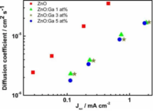
The electron diffusion coefficients in DSCs with and
without Ga-modified ZnO electrodes are shown in Fig. 3.
The gallium modification brought about a twofold decrease
in the values of D. The decrease in D might be a
conse-quence of a higher trap density in ZnO:Ga in comparison to
TABLE I. Roughness factor and parameters from theJ-Vcurves共AM 1.5, 100 mW cm−2兲measured from sealed DSCs based on 6-m-thick ZnO and
ZnO:Ga electrodes. Average cell area: 0.15 cm2.
DSC
Roughness factor 共%兲
Dye loading 共mol cm−2兲
Jsc 共mA cm−2兲
Voc 共V兲
ZnO 274 ⬍1⫻10−8 2.07 0.79
ZnO:Ga 1 at% 365 6⫻10−8 5.32 0.79
ZnO:Ga 3 at% 389 6.5⫻10−8 5.56 0.79
ZnO:Ga 5 at% 483 8.1⫻10−8 6.49 0.79
FIG. 1. 共Color online兲 Typical photovoltage transient induced by the stepped laser intensity. The inset shows a typical photocurrent transient from SLIM-PCV measurements. Both photovoltage and photocurrent transients were observed for DSCs based on a ZnO:Ga 3 at%electrode.
ZnO electrodes and/or a higher resistance at the interparticle boundaries. The increase in trap density would arise from the higher surface area of ZnO:Ga electrodes compared to that of
the ZnO electrode and/or from the introduction of Ga3+ as
intraband states. Since electrons spend more time in traps,
the values ofDbecome smaller. Indeed, measurements from
impedance spectroscopy for the same DSCs reported herein evidenced a higher chemical capacitance for DSCs based on
ZnO:Ga compared to the ZnO-based analogs.32 Such higher
chemical capacitance in ZnO:Ga is believed to arise from the higher surface area, porosity, roughness factor, and point de-fect density.32
Additional data from the XPS spectra of ZnO and ZnO:Ga photoelectrodes showed the presence of gallium as
Ga3+in ZnO:Ga powder samples by the characteristic
bind-ing energies.27Therefore, it is believed that some of the Ga3+ ions seem to substitute for Zn2+ions in the wurtzite
hexago-nal structure of ZnO共Ref.27兲or occupy the position of zinc vacancies.21However, the possibility of some Ga3+ions
act-ing in the surface modification of ZnO cannot be ruled out.
The electron lifetime values 共兲 obtained from
photo-voltage transients are shown in Fig.4. In the case of, gal-lium modification provided DSCs with a longer electron
life-time than those in ZnO-based ones, as expected from theD
values 共Fig. 3兲. This can be rationalized in terms of
diffusion-limited electron lifetimes; that is, trapped electrons do not recombine with I3
−
, and, thus, an increase in trapped time results in a decrease in recombination rate. The results
in Figs. 3 and4are also similar to those reported by Kopi-dakis et al.33 In their report, Li+ ions intercalated into the
TiO2 and the cations acted as charge traps, decreasing the
electron diffusion coefficient and recombination rate. An-other report shows that the decrease inDand the increase in
with smaller TiO2 particle sizes were interpreted in terms
of a larger film surface area and a higher number of particle boundaries, where charge trap sites are likely to exist.34
Figure5 shows theVoc as a function of photogenerated
electron density. Note that the porosity of the film was not taken into account to determine the electron density. The
ZnO:Ga-based DSCs showed a lower Voc at matched
elec-tron densities. This might be associated with the positive shift of the conduction band edge 共ECB兲and the increase in
trap density. However, by taking porosity into account to explain the decrease inVocat matched electron densities, the
trap density could be increased by a factor of 6–8. On the other hand, the roughness factor was only doubled. With the results of the decrease in Dby a factor of 2, it is not
suffi-cient to explain the lower Voc only by the change in trap
density. As mentioned previously, TAS data from our group suggested a higher charge injection yield for the case of ZnO:Ga electrodes.27This suggests that the conduction band edge of ZnO was shifted positively by the addition of Ga ions. Thus, the lower Voc at the matched electron density is
probably caused by both the increase in trap density and the positive shift of the conduction band edge. TableIshows that
the Vocwas the same regardless of Ga modification under 1
FIG. 2. 共Color online兲Behavior ofVocandJscfrom SLIM-PCV
measure-ments for DSCs based on ZnO and ZnO:Ga 1, 3, and 5 at% electrodes under open-circuit conditions at different illumination intensities. The bot-tom axis showsJscvalues measured under the same laser intensity used for
the photovoltage transient measurements.
FIG. 3. 共Color online兲 Diffusion coefficient under different illumination intensities from SLIM-PCV measurements in DSCs based on N-719-sensitized ZnO and ZnO:Ga electrodes共film thickness: 6 m兲.
FIG. 4. 共Color online兲 Electron lifetimes determined from photovoltage transients under open-circuit conditions at different illumination intensities. The bottom axis showsJscvalues measured under the same laser intensity
used for the photovoltage transient measurements.
sun illumination. This can be well explained by a higher electron density in ZnO:Ga than in ZnO due to the longer electron lifetime of the former.
IV. CONCLUSIONS
The studies of photocurrent and photovoltage transients showed that the electron diffusion coefficients in ZnO elec-trodes were decreased, while the electron lifetimes were in-creased, after a gallium modification of the ZnO electrode. This behavior was interpreted according to the increase in intraband charge traps in the nanoporous electrodes. The
lowerVocof DSCs using Ga-modified ZnO at matched
elec-tron density is probably caused not only by the increased intraband trap density but also by the positive shift of the
ZnO:Ga conduction band edge. The higher Jsc values
ob-served in ZnO:Ga-based DSCs were assigned to higher charge injection efficiencies, resulting mainly from the posi-tive shift of the ZnO:Ga conduction band edge, in addition to the higher roughness factor of the electrode.
ACKNOWLEDGMENTS
The authors thank Capes, Renami, CNPq, and Fapesp for the financial support. Professor Dr. Carol H. Collins is gratefully acknowledged for English revision.
1
B. O’Regan and M. Gratzel,Nature共London兲353, 737共1991兲. 2
Q. Wang, S. Ito, M. Gratzel, F. Fabregat-Santiago, I. Mora-Sero, J. Bisquert, T. Bessho, and H. Imai,J. Phys. Chem. B110, 25210共2006兲.
3
J. van de Lagemaat, N. G. Park, and A. J. Frank,J. Phys. Chem. B104,
2044共2000兲.
4
K. Schwarzburg and F. Willig,J. Phys. Chem. B103, 5743共1999兲. 5
J. Nelson,Phys. Rev. B59, 15374共1999兲.
6
N. Kopidakis, E. A. Schiff, N. G. Park, J. van de Lagemaat, and A. J. Frank,J. Phys. Chem. B104, 3930共2000兲.
7
J. van de Lagemaat and A. J. Frank,J. Phys. Chem. B105, 11194共2001兲.
8
N. Kopidakis, N. R. Neale, K. Zhu, J. van de Lagemaat, and A. J. Frank,
Appl. Phys. Lett.87, 202106共2005兲.
9
S. Mori, K. Sunahara, Y. Fukai, T. Kanzaki, Y. Wada, and S. Yanagida,J. Phys. Chem. C112, 20505共2008兲.
10
Y. Diamant, S. Chappel, S. G. Chen, O. Melamed, and A. Zaban,Coord.
Chem. Rev.248, 1271共2004兲. 11
K. H. Ko, Y. C. Lee, and Y. J. Jung,J. Colloid Interface Sci.283, 482 共2005兲.
12
T. Ma, M. Akiyama, E. Abe, and I. Imai,Nano Lett.5, 2543共2005兲.
13
L. Schmidt-Mende and J. L. MacManus-Driscoll,Mater. Today 10, 40 共2007兲.
14
M. Law, L. E. Greene, J. C. Johnson, R. Saykally, and P. Yang,Nature Mater.4, 455共2005兲.
15
E. Galoppini, J. Rochford, H. Chen, G. Saraf, Y. Lu, A. Hagfeldt, and G. Boschloo,J. Phys. Chem. B110, 16159共2006兲.
16
P. Jiang, J. J. Zhou, H. F. Fang, C. Y. Wang, Z. L. Wang, and S. S. Xie,
Adv. Funct. Mater.17, 1303共2007兲.
17
C. Y. Jiang, X. W. Sun, G. Q. Lo, D. L. Kwong, and J. X. Wang,Appl. Phys. Lett.90, 263501共2007兲.
18
J. Liu and X. Huang,J. Solid State Chem.179, 843共2006兲.
19
A. B. F. Martinson, J. W. Elam, J. T. Hupp, and M. J. Pellin,Nano Lett.7,
2183共2007兲.
20
H. Chen, A. D. Pasquier, G. Saraf, J. Zhong, and Y. Lu,Semicond. Sci. Technol.23, 045004共2008兲.
21
H. Wang, S. Baek, J. Song, J. Lee, and S. Lim, Nanotechnology 19,
075607共2008兲.
22
A. de Souza Gonçalves, S. A. M. de Lima, M. R. Davolos, S. G. Antonio, and C. de Oliveira Paiva-Santos,J. Solid State Chem.179, 1330共2006兲.
23
D. Look,J. Electron. Mater.35, 1299共2006兲.
24
S. Cimitan, S. Albonetti, L. Forni, F. Peri, and D. Lazzari, J. Colloid Interface Sci.329, 73共2009兲.
25
R. P. Wang, A. W. Sleight, and D. Cleary,Chem. Mater.8, 433共1996兲.
26
J. J. Robbins, C. Fry, and C. A. Wolden,J. Cryst. Growth263, 283共2004兲. 27
A. de Souza Gonçalves, M. R. Davolos, N. Masaki, S. Yanagida, A. Mo-randeira, J. R. Durrant, J. N. Freitas, and A. F. Nogueira,Dalton Trans. 2008, 1487.
28
K. Keis, L. Vayssieres, H. Rensmo, S. E. Lindquist, and A. Hagfeldt,J. Electrochem. Soc.148, A149共2001兲.
29
S. Nakade, T. Kanzaki, Y. Wada, and S. Yanagida,Langmuir21, 10803 共2005兲.
30
K. Kakiuchi, E. Hosono, and S. Fujihara,J. Photochem. Photobiol., A179,
81共2006兲.
31
G. Schlichthorl, S. Y. Huang, J. Sprague, and A. J. Frank,J. Phys. Chem. B101, 8141共1997兲.
32
A. D. Gonçalves, M. S. Góes, F. Frabregat-Santiago, T. Mohel, M. R. Davolos, J. Bisquert, S. Yanagida, A. F. Nogueira, and P. R. Bueno, “Den-sity of states and charge lifetime in dye-sensitized solar cells based on ZnO:Ga nanostructured photoanodes,” 2009共unpublished兲.
33
N. Kopidakis, K. D. Benkstein, J. van de Lagemaat, and A. J. Frank,J. Phys. Chem. B107, 11307共2003兲.
34
S. Nakade, Y. Saito, W. Kubo, T. Kitamura, Y. Wada, and S. Yanagida,J. Phys. Chem. B107, 8607共2003兲.