PAPER
www.rsc.org/dalton
| Dalton Transactions
Synthesis and characterization of ZnO and ZnO:Ga films and their
application in dye-sensitized solar cells
Agnaldo de Souza Gonc¸alves,*
aMarian Rosaly Davolos,
aNaruhiko Masaki,
bShozo Yanagida,
bAna Morandeira,
cJames R. Durrant,
cJilian Nei Freitas
dand Ana Fl´avia Nogueira*
dReceived 31st October 2007, Accepted 4th January 2008
First published as an Advance Article on the web 12th February 2008
DOI: 10.1039/b716724e
Highly crystalline ZnO and Ga-modified zinc oxide (ZnO:Ga) nanoparticles containing 1, 3 and 5 atom% of Ga3+were prepared by precipitation method at low temperature. The films were characterized
by XRD, BET, XPS and SEM. No evidence of zinc gallate formation (ZnGa2O4), even in the samples
containing 5 atom% of gallium, was detected by XRD. XPS data revealed that Ga is present into the ZnO matrix as Ga3+, according to the characteristic binding energies. The particle size decreased as the
gallium level was increased as observed by SEM, which might be related to a faster hydrolysis reaction rate. The smaller particle size provided films with higher porosity and surface area, enabling a higher dye loading. When these films were applied to dye-sensitized solar cells (DSSCs) as photoelectrodes, the device based on ZnO:Ga 5 atom% presented an overall conversion efficiency of 6% (at 10 mW cm−2), a
three-fold increase compared to the ZnO-based DSSCs under the same conditions. To our knowledge, this is one of the highest efficiencies reported so far for ZnO-based DSSCs. Transient absorption (TAS) study of the photoinduced dynamics of dye-sensitized ZnO:Ga films showed that the higher the gallium content, the higher the amount of dye cation formed, while no significant change on the recombination dynamics was observed. The study indicates that Ga-modification of nanocrystalline ZnO leads to an improvement of photocurrent and overall efficiency in the corresponding device.
Introduction
Great attention has been devoted to solar energy conversion by dye-sensitized solar cells (DSSCs) since the pioneering work reported by O’Regan and Gr¨atzel,1 especially in light of their
low cost compared to conventional silicon solar cells. The device compromises a working electrode (usually a wide band gap semiconductor deposited in the form of a porous nanostructured film onto a transparent conductor oxide-TCO) sensitized by a ruthenium complex, usually the N3 or N-719 dye. This electrode is separated from the counter electrode (generally a Pt film deposited on a TCO) by an electrolyte (usually I3−/I−in a mixture of organic
solvents). DSSCs based on TiO2as the nanostructured electrode
are capable of achieving efficiencies of 11%.2
Despite the fact that much work relies on DSSCs based on pure photoelectrodes,i.e., not intentionally doped oxides such as TiO2and ZnO, some recent
works have revealed high efficiencies obtained with nitrogen-doped titania electrode3and (Al + W)-doped TiO
2.
4ZnO is a wide
band gap semiconductor (∼3.2 eV at room temperature) whose n-type behavior stems from its intrinsic oxygen deficiency
(non-aInstituto de Qu´ımica, Universidade Estadual Paulista-UNESP, Araraquara,
SP, Brazil
bCenter for Advanced Science and Innovation, Osaka University, Suita,
Osaka, 565-0871, Japan
cCentre for Electronic Materials and Devices, Imperial College of Science
Technology and Medicine, London, UK SW7 2AY
dInstituto de Qu´ımica, Universidade Estadual de Campinas-UNICAMP,
Campinas, SP, Brazil. E-mail: [email protected]; Fax: +55 19 3521 3023; Tel: +55 19 3521 3029
stoichiometric oxide). Among their wide range of applications, ZnO films have potential to be applied as an alternative material for nanostructured electrodes in photoelectrochemical solar cells.5
The DSSCs based on ZnO have their solar conversion efficiencies limited, in part, by the formation of Zn2+/dye aggregates during
the dye loading process depending on the dye composition, concentration and sensitization time.6 As reported earlier, the
electron injection is decreased by the presence of aggregates on the surface of ZnO films.7Besides, the molecules that are active for
electron injection are attached directly to the ZnO surface while the aggregates are formed on this layer, according to the microscopic image of transient absorption.8One reason for the improvement in
the overall solar cell efficiency from 2 to 5% (AM 1.5, 10 mW cm−2)
in DSSCs based on ZnO was the controlled dye-sensitization step through the addition of base to the dye solution or by shortening the sensitization time.6Recently, the improvement of dye-loading
in photoanodes came about by changing the microstructure of ZnO films5 yielding a conversion efficiency of 4.1% (AM 1.5,
100 mW cm−2) and 4.6% at low light power density (AM 1.5,
14 mW cm−2).
Although the strategy of doping the oxide semiconductors has generated promising results for TiO2 films,
3,4 the doping of
ZnO with aluminium did not produce DSSCs with improved performance.9,10
Minami et al. have attempted to decrease the electric resistance of ZnO films by doping of group III elements such as B, Al, Ga and In.11Indeed, they reported an increase in
carrier concentration after doping.11A myriad of applications such
as transparent conductor oxide, laser diodes,etc.take advantage of the lower resistivity brought about by doping.12Nonakaet al.,
using molecular orbital calculations, demonstrated that new states originating from group III elements appear within the band gap.13
In this work we report DSSCs based on gallium-modified zinc oxide electrodes (ZnO:Ga) with improved efficiencies in comparison to pure ZnO based solar cells. In order to have more clear evidence of the gallium modification effect on the photovoltaic properties and on the film energetics, transient absorption spectroscopy (TAS) was used as a tool to probe the charge recombination dynamics in these films.
Experimental
ZnO and ZnO:Ga 1, 3 and 5 atom% nanoparticles were syn-thesized by adapting the procedure described in the literature.9
Zinc nitrate aqueous solution (0.1 mol L−1at pH 5) was mixed
with 0.1 mol L−1triethanolamine. Gallium nitrate was used as the
source of the Ga3+. The powder samples were characterized by
X-ray diffractometry (XRD) using a Rigaku RINT 2000 (copper target,k= 1.5406 A˚ ). The colloidal solution was obtained by mixing ZnO or ZnO:Ga powder, deionized water, acetylacetone and Triton X-100. The resulting mixture was ground in a mortar forca.1 h. The paste was then applied on the conducting substrate (fluorine-doped SnO2glass, FTO) by the doctor blading technique.
Adhesive tape (Scotch) was used as frame and spacer. The semi-R conductor film was heated at 450◦C for 30 min to provide adequate
electrical contact between the particles. The electrodes, while still warm (ca.80◦C), were immersed into a 0.5 mmol L−1ethanolic
solution of the complex [cis-bis(isothiocyanato)bis(2,2′ -bipyridyl-4,4′-dicarboxylate]ruthenium(
II) bis-tetrabutylammonium (also known as N-719, Solaronix) for 3 h at room temperature. Then, the sensitized films were rinsed with absolute ethanol to remove non-adsorbed N-719 species and allowed to dry in air. The liquid electrolyte was composed of 0.1 mol L−1 LiI, 0.05 mol L−1 I
2,
0.8 mol L−1 tetrabutylammonium iodide, 0.5 mol L−1
4-tert-butylpyridine in 50% acetonitrile–50% 3-methoxypropionitrile. A Pt-sputtered FTO was used as the counter electrode. The cells were sealed by Himilan (Mitsui-Dupont Polychemicals). Film thickness was 6lm (measured by the Sloan Technology profiler, Dektak 3) and the average cell area was 0.15 cm2. The electrode morphology
was observed by field emission scanning electron microscopy (SEM, Jeol JSM-6700FE). The X-ray photoelectron spectroscopy (XPS) was performed in a QuanteraSXM PHI instrument using the Al-Ka monochromatized X-ray source. The porosity and average pore size were estimated by the BET method based on nitrogen adsorption isotherm (Quantachrome, Autosorb 1) after scratching the films off the FTO. The pore size distribution estimated for the ZnO electrode was not clearly identified. Dye loading was determined according to a published procedure.5The
dye was desorbed from the porous film by using a 1 mol L−1NaOH
solution (water–ethanol 1 : 1 volume ratio) and then analyzed in a UV-Vis Shimadzu UV-2500PC spectrophotometer according to the absorbance data of N-719 standard solutions.
The J–V curves of the sealed cells were measured under AM 1.5 illumination (100 mW cm−2) using a solar simulator
(Yamashita Denso, YSS-80). The electrodes were illuminated from the substrate–electrode side. The incident photon to current conversion efficiency (IPCE) was measured by using a commercial setup (PV-25DYE, JASCO). The data fromJ–Vcurves and action
spectra represent the average behaviour for at least four cells of each sample.
The transient absorption (TAS) decays in thels–ms timescale were measured on dye-sensitized electrodes. The setup has been described elsewhere.14
The study of the dye-sensitized films in a redox-inactive electrolyte (propylene carbonate) was carried out setting the excitation at 550 nm and monitoring the optical changes at a probe wavelength of 800 nm, whose amplitude is primarily dominated by dye cation absorption.15Data were collected in the
absence of an applied bias voltage under low-intensity excitation pulses corresponding approximately one injected electron per colloidal particle16 (average absorbance at the dye absorption
maximum was 0.3). The TAS data for the pristine ZnO film were not possible to be measured because of its low transmittance.
Results and discussion
In the gallium-doped zinc oxide (ZnO:Ga), Ga3+ is expected to
cause only a small lattice distortion because of their similar tetrahedral radii. Ga3+ions also act as an efficient shallow donor in
ZnO. However, gallium doping might give rise to spinel structures (MIIGa
2O4) when the matrix to be doped is ZnO, especially when
heavily doped samples are taken into account.17
Solubility limits are reported to be close to 3 atom% of Ga in ZnO.18,19 The
formation of ZnGa2O4 might take place in ZnO:Ga, changing
the microscopic structural and electronic environment of Ga3+in
the ZnO matrix. In the normal cubic spinel crystal structure of ZnGa2O4, Zn2+ions occupy tetrahedral sites and Ga3+ ions the
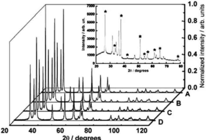
octahedral ones. The powder X-ray diffraction (XRD) patterns of pure and gallium-modified zinc oxide (ZnO:Ga) nanoparticles are shown in Fig. 1. All samples have the zincite structure (JCPDS 14– 3651) and there is no evidence of zinc gallate formation (ZnGa2O4),
even in the ZnO:Ga 5 atom% nanoparticles.
Fig. 1 Powder X-ray diffraction patterns of the nanoparticles synthesized by the precipitation method: (A) ZnO, (B) ZnO:Ga 1 atom%, (C) ZnO:Ga 3 atom% and (D) ZnO:Ga 5 atom%. Inset: X-ray diffraction pattern of the ZnO:Ga 5 atom% porous film. Asterisks denote FTO reflections.
The absence of ZnGa2O4 in the XRD patterns of ZnO:Ga
nanoparticles is probably related to the low-temperature treatment employed: 150 ◦C for 2 h. The high crystallinity observed
in the XRD patterns indicates the capability of preparing
nanocrystalline samples at low temperature by using the precipi-tation method.
The possibility of ZnGa2O4formation in the porous film (after
the heat treatment at 450◦C for 30 min) was also evaluated by
XRD. The XRD pattern of the ZnO:Ga 5 atom% porous film deposited onto an FTO substrate is shown in Fig. 1 (see inset). Despite the FTO reflections it is possible to observe only the ZnO diffraction patterns, which indicates that ZnGa2O4is not present
in the gallium-modified zinc oxide porous electrodes even after the thermal treatment. The morphology of the films was analyzed by SEM (Fig. 2).
Fig. 2 FE-SEM images of the ZnO and ZnO:Ga electrodes: (A) ZnO, (B) ZnO:Ga 1 atom%, (C) ZnO:Ga 3 atom% and (D) ZnO:Ga 5 atom%.
The ZnO:Ga films present smaller particle size than the ZnO electrode, as already observed for undoped TiO2 compared to
doped TiO2powders.
4This behavior was associated to an increased
hydrolysis reaction rate for doped TiO2 powders.
4 A higher
hydrolysis reaction rate is also believed to give rise to smaller particles of the gallium-modified samples in this work.
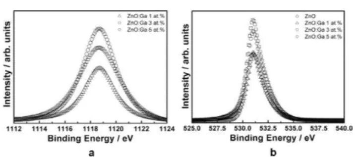
XPS data (Fig. 3) reveal a Ga 2p3/2peak located at 1119.0 eV, in
good agreement with other reported values.20,21This is an evidence
that Ga ions exist as Ga3+into the ZnO matrix. The intensity of
the peak increases as the content of Ga3+ in the sample is also
increased. Ga3+ions are believed to be incorporated into the Zn2+
sites due to their radii similarity, leading to a substitutional doping. No shift in the O 1s spectra (Fig. 3(b)) was observed, further evidencing the absence of a spurious phase related to Ga2O3or
even ZnGa2O4.
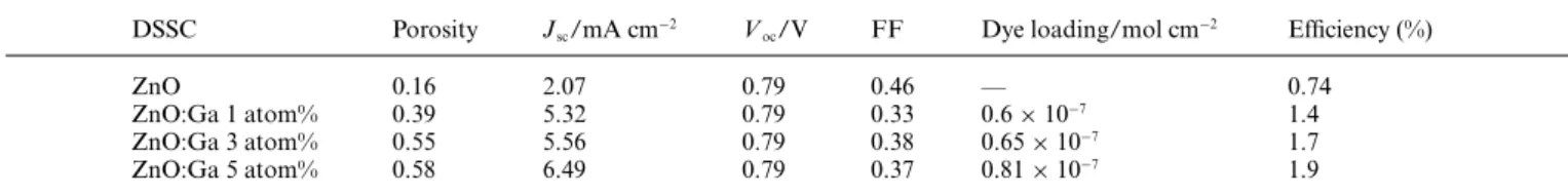
The average pore size of the ZnO:Ga electrodes was estimated from the BET method. The electrodes based on ZnO:Ga 5 atom% present a relatively smaller and narrower pore size distribution than ZnO:Ga 1 and 3 atom%. The average pore size of ZnO:Ga 5 atom% electrodes was estimated to be 26 and ∼60 nm for ZnO:Ga 1 and 3 atom% electrodes, respectively. As observed in Table 1, the porosity increases with the increase in Ga3+content.
It is important to point out here that all samples, pristine and gallium-modified ZnO, were prepared using the same experimental procedure. Further improvements in the synthesis and deposition method are believed to enhance both porosity and adhesion of all samples to the TCO, respectively.
Fig. 3 Core level XPS spectra: (a) Ga 2p and (b) O 1s (Al-KaX-ray
source).
TheJ–V curves of the DSSCs based on ZnO and ZnO:Ga 1, 3 and 5 atom% under illumination of 100 mW cm−2 are shown
in Fig. 4. Table 1 also summarizes theJ–V characteristics of the sealed DSSCs and the amount of ruthenium dye absorbed for each electrode.
Fig. 4 J–Vcurves (AM 1.5, illumination intensity of 100 mW cm−2) of
the sealed DSSCs based on ZnO and ZnO:Ga 1, 3 and 5 atom% films
(6lm) sensitized for 3 h in 0.5 mmol L−1N-719 dye solution. Inset:J–V
curve of a DSSC based on ZnO:Ga 5 atom% with film thickness of 20lm
under 10 mW cm−2.
Values of open circuit voltage (Voc) are close to 0.8 V, which
are comparable to TiO2-based solar cells. Considering the film
thickness employed (6lm), the amount of ruthenium dye absorbed here is comparable to a 10lm thick TiO2 electrode (g= 10%)
sensitized by the N-3 dye22(1.3
×10−7mol cm−2) and also to a
20lm thick ZnO/N-719 photoanode5(1.4×10⁻⁷mol cm−2). The
gallium modification resulted in more than a two-fold increase in photocurrent compared to the pristine ZnO. The DSSC based on ZnO:Ga 5 atom% provided the highest photocurrent density indicating that gallium modification enables the preparation of electrodes with better electronic properties compared to non-intentionally modified ZnO. The higher photocurrent might, in part, be related to a large contribution to the density of states of ZnO arising from Ga 3s states, especially due to their energetically highly delocalized nature near the Fermi level.23 Conversion
efficiencies (g) of 6% were achieved at a low light power density (10 mW cm−2) for cells based on ZnO:Ga 5 atom% with film
thickness of 20lm (Fig. 4, inset). This is one of the highest values reported so far for DSSCs based on ZnO systems under similar conditions. Kakiuchiet al.reported agvalue of 4.6% under 14 mW
Table 1 Performance features from J–V curves of DSSCs based on ZnO, ZnO:Ga 1, 3 and 5 atom% porous nanostructured electrodes under
100 mW cm−2, along with porosity data and dye loading
DSSC Porosity Jsc/mA cm−2 Voc/V FF Dye loading/mol cm−2 Efficiency (%)
ZnO 0.16 2.07 0.79 0.46 — 0.74
ZnO:Ga 1 atom% 0.39 5.32 0.79 0.33 0.6×10⁻⁷ 1.4
ZnO:Ga 3 atom% 0.55 5.56 0.79 0.38 0.65×10⁻⁷ 1.7
ZnO:Ga 5 atom% 0.58 6.49 0.79 0.37 0.81×10⁻⁷ 1.9
cm−2for a DSSC based on a 20
lm thick ZnO/N-719 photoanode.5 The low FF values reported here might be a consequence of the high series resistance losses arising from the poor adhesion between the ZnO:Ga nanoparticles and the TCO substrate.
The IPCE curves of the DSSCs based on ZnO and ZnO:Ga resemble the absorption spectrum of the ruthenium dye (Fig. 5). An IPCE value of 20% was achieved by the DSSC based on ZnO:Ga 5 atom%.
Fig. 5 IPCE curves (action spectra) of DSSCs based on ZnO and ZnO:Ga 1, 3 and 5 atom% as the nanostructured porous electrodes.
An improvement in the adhesion of the ZnO:Ga nanoparticles to the TCO substrate is expected to increase these efficiencies. An interesting difference in these action spectra and those usually reported for DSSCs based on TiO2is observed at long wavelengths.
The low IPCE values around 700 nm, is an evidence of poor electron injection at long wavelengths due to the slightly higher conduction band edge of ZnO compared to TiO2. This effect will
be discussed in further detail in a future publication.
To address the effect of the gallium modification on the zinc dissolution and to analyse how this can affect the amount of ruthenium dye absorbed, and as a consequence, the formation of dye aggregates, two equal volumes of buffer solution (Synth, pH 4) were added to two vessels at room temperature. A non-sensitized ZnO porous film at temperature around 80 ◦C was
immersed into the buffer solution and the same procedure was done simultaneously using a ZnO:Ga 5 atom% porous film. The immersion time was 3 h (equal to the sensitization time used in this work). After this period both ZnO and ZnO:Ga 5 atom% films were completely dissolved. Therefore, gallium doping does not affect the solubility of ZnO films.
Fig. 6 shows the charge recombination decays fromls to ms for the ZnO:Ga films using a redox inactive electrolyte. Transient data were collected at 800 nm, monitoring the induced absorption of dye cations generated by electron injection into the ZnO:Ga films.
Fig. 6 Transient absorption spectra of ZnO:Ga porous films sensitized by the N-719 dye: (a) ZnO:Ga 5 atom%, (b) ZnO:Ga 3 atom% and (c) ZnO:Ga 1 atom%. The probe wavelength was 800 nm, where the signal is mainly due to the dye radical cation absorption. The excitation wavelength was 550 nm.
The characteristic non-exponential kinetics reported for TiO2
and ZnO electrodes24 is also observed here, indicating that the
recombination dynamics are controlled by electron transport through an energetic distribution of trap states within the metal oxide film.25The recombination half time values,
t50%, observed in
this work are∼300ls, a little faster than typical values reported for TiO2electrodes25(800ls) but slower than those measured for
SnO2(4ls).25
The increase in the amplitude of the transient absorption signal with gallium level is striking, indicating an order of magnitude increase in the yield of dye cations with increased Ga density. This increase in amplitude appears to be significantly larger than the increase in the amount of ruthenium dye absorbed, and therefore can not be attributed primarily to an increase in light absorption. Rather, the observed increase in the dye cation yield suggests more efficient electron injection from the dye excited state. Such more efficient electron injection most plausibly stems from faster electron injection kinetics due to an increase of the number of acceptor states in the semiconductor. This increased electron injection yield correlates well with the increase in photocurrent density.
Conclusions
The gallium modification in ZnO produced a smaller particle size, higher porosity and surface area. No evidence of ZnGa2O4 or
any other contaminant phase was observed even in the ZnO:Ga 5 atom% porous film. As evidenced from the characteristic binding energies, Ga is present in the ZnO matrix as Ga3+. The increase
in dye cation yield observed by TAS indicated a more efficient
electron injection from the dye excited state, possibly associated with a faster electron injection kinetics. High performance DSSCs may be assembled based on ZnO:Ga porous nanostructured electrodes with agvalue as high as 6% at low light intensity.
Acknowledgements
We thank Fapesp, CNPq and Renami for the financial support. A. S. G. and J. N. F. thank Fapesp for the scholarships. A. S. G. thanks Capes for the scholarship and Brian O’Regan for helpful discussions. The authors also thank C. O. Paiva-Santos and S. G. Ant ˆonio for the XRD measurements.
References
1 B. O’Regan and M. Gratzel,Nature, 1991,353, 737–740.
2 J. M. Kroon, N. J. Bakker, H. J. P. Smit, P. Liska, K. R. Thampi, P. Wang, S. M. Zakeeruddin, M. Gratzel, A. Hinsch, S. Hore, U. Wurfel, R. Sastrawan, J. R. Durrant, E. Palomares, H. Pettersson, T. Gruszecki,
J. Walter, K. Skupien and G. E. Tulloch,Prog. Photovoltaics, 2007,15,
1–18.
3 T. Ma, M. Akiyama, E. Abe and I. Imai,Nano Lett., 2005,5, 2543–
2547.
4 K. H. Ko, Y. C. Lee and Y. J. Jung,J. Colloid Interface Sci., 2005,283,
482–487.
5 K. Kakiuchi, E. Hosono and S. Fujihara,J. Photochem. Photobiol., A,
2006,179, 81–86.
6 K. Keis, E. Magnusson, H. Lindstrom, S.-E. Lindquist and A. Hagfeldt,
Sol. Energy Mater. Sol. Cells, 2002,73, 51–58.
7 H. Horiuchi, R. Katoh, K. Hara, M. Yanagida, S. Murata, H. Arakawa
and M. Tachiya,J. Phys. Chem. B, 2003,107, 2570–2574.
8 R. Katoh, A. Furube, Y. Tamaki, T. Yoshihara, M. Murai, K. Hara,
S. Murata, H. Arakawa and M. Tachiya,J. Photochem. Photobiol., A,
2004,166, 69–74.
9 K. Keis, L. Vayssieres, H. Rensmo, S.-E. Lindquist and A. Hagfeldt,
J. Electrochem. Soc., 2001,148, A149–A155.
10 H. Rensmo, K. Keis, H. Lindstrom, S. Sodergren, A. Solbrand, A.
Hagfeldt, S. E. Lindquist, L. N. Wang and M. Muhammed,J. Phys.
Chem. B, 1997,101, 2598–2601.
11 T. Minami, H. Sato, H. Nanto and S. Takata,Jpn. J. Appl. Phys., 1985,
24, L781–L784.
12 S.-M. Park, T. Ikegami and K. Ebihara,Thin Solid Films, 2006,513,
90–94.
13 M. Nonaka, S. Matsushima, M. Mizuno and K. Kobayashi,Chem.
Lett., 2002, 580–581.
14 H. Ohkita, S. Cook, T. A. Ford, N. C. Greenham and J. R. Durrant,
J. Photochem. Photobiol., A, 2006,182, 225–230.
15 S. A. Haque, Y. Tachibana, R. L. Willis, J. E. Moser, M. Gratzel, D. R.
Klug and J. R. Durrant,J. Phys. Chem. B, 2000,104, 538–547.
16 S. A. Haque, Y. Tachibana, D. R. Klug and J. R. Durrant,J. Phys.
Chem. B, 1998,102, 1745–1749.
17 A. S. Gonc¸alves, S. A. M. Lima, M. R. Davolos, S. G. Ant ˆonio and
C. O. Paiva-Santos,J. Solid State Chem., 2006,179, 1330–1334.
18 N. Roberts, R. P. Wang, A. W. Sleight and W. W. Warren,Phys. Rev. B,
1998,57, 5734.
19 R. Wang, A. W. Sleight and D. Cleary,Chem. Mater., 1996,8, 433–
439.
20 M. Passlack, E. F. Schubert, W. S. Hobson, M. Hong, N. Moriya, S. N. G. Chu, K. Konstadinidis, J. P. Mannaerts, M. L. Schnoes and
G. J. Zydzik,J. Appl. Phys., 1995,77, 686–693.
21 V. Bhosle, A. Tiwari and J. Narayan,J. Appl. Phys., 2006,100, 033713–
033716.
22 M. K. Nazeeruddin, A. Kay, I. Rodicio, R. Humphrybaker, E. Muller,
P. Liska, N. Vlachopoulos and M. Gratzel,J. Am. Chem. Soc., 1993,
115, 6382–6390.
23 Y. Imai and A. Watanabe,J. Mater. Sci., 2005,15, 743–749.
24 R. L. Willis, C. Olson, B. O’Regan, T. Lutz, J. Nelson and J. R. Durrant,
J. Phys. Chem. B, 2002,106, 7605–7613.
25 A. N. M. Green, E. Palomares, S. A. Haque, J. M. Kroon and J. R.
Durrant,J. Phys. Chem. B, 2005,109, 12525–12533.