Efficient passive network description of IC conducted emission
models for model reduction
S. Ludwig1,2, Lj. Radi´c-Weissenfeld1,2, W. Mathis1, and W. John2
1Leibniz University of Hannover, Institute of Electromagnetic Theory, Hannover, Germany
2Fraunhofer Institute for Reliability and Microintegration Advanced System Engineering, Paderborn, Germany
Abstract. This article adresses the model reduction of IC conducted emission models. A method to efficiently deal with the high number of independent sources in IC conducted emission models, which are a strong limitation for model or-der reduction, is presented. A network alteration is proposed, which allows for a much higher model reduction than stan-dard approaches. The system of the altered network can be more efficiently reduced with standard model order reduc-tion algorithms in order to speed up frequency-simulareduc-tions. Synthesising the reduced system into a passive electrical net-work enables fast time-simulations to be made with circuit simulators. The whole procedure is validated by reducing an example of an IC conducted emission model of an 32 Bit mi-crocontroller.
1 Introduction
With decreasing size of device structures additional effects have to be considered early in the design process (Helle-brandt et al., 2007; John, 2004). Electrical models for IC conducted emission are created to help semiconductor manu-facturers to take on-chip EMC effects into account during the design process. The IC conducted emission models typically contain up to many thousands of resistors, inductors, capaci-tors and independent current sources, which results in a high complexity and leads to long simulation times. A smaller model, which engulfs the main properties and enables faster simulations, can be achieved by applying a model order re-duction (MOR) (Antoulas, 1998; Radi´c et al., 2008).
In this article an efficient network description of the IC conducted emission model, which enables a high order re-duction, is introduced.
Correspondence to:S. Ludwig ([email protected])
The IC conducted emission model is introduced in Sect. 2. The description of the model as a system of circuit equations is exhibited in Sect. 3. The standard as well as the proposed network description of the model are shown in Sect. 4. In Sect. 5 the used MOR method is presented. A reduced model is created by synthesising the order reduced system into an electrical network as described in Sect. 6. The validity of the proposed model reduction is shown with an example in Sect. 7 and finally the article is concluded in Sect. 8.
2 IC conducted emission model
IC conducted emission models are used for the modelling of the on-chip EMC behaviour. These models consist of pas-sive elements as well as independent current sources with a prescribed current waveform (Dhia et al., 2006). The passive R, L, C elements model the parasitic electromagnetic effect, while the independent sources represent the internal currents, generated due to the switching of the transistors. The param-eters of the model are determined either during the IC design phase or by taking measurements on an existing chip (Dhia et al., 2006; Hesidenz and Steinecke, 2005). Due to the com-plexity of an IC the conducted emission model consists of hundreds of equal substructures for every block of the IC, e.g. digital, analogue or memory blocks (Hesidenz and Stei-necke, 2005), as seen in Fig. 1.
Fig. 1.Section of the IC conducted emission model.
3 Circuit equations
For MOR the electrical network of the IC conducted emis-sion model has to be described with the help of the modified nodal analysis as a system of differential algebraic equations, in the form of
(sC+G)x=Bu, y=LTx. (1) Vectorsuǫℜpandyǫℜr in Eq. (1) are the input and output re-spectively, which are connected with the system vectorxǫℜN
by the system matricesBǫℜN×pandLǫℜN×r. N is the or-der of the system,pthe number of inputs andrthe number of outputs. Typically one electrical value at the port is the in-put and the dual value is the outin-put, so thatB=Landr=p hold. Symmetric system matricesCǫℜN×N andGǫℜN×N
contain the stamps for capacitors, resistors and the inductors. The transfer function of the system is
H(s)=LT(sC+G)−1B. (2)
4 Efficient network description of the IC conducted emission model
For the description of the IC conducted emission model in circuit equations inputs and outputs of the system have to be defined. In standard approaches the nodes of the indepen-dent current sources are described as ports (Silva et al., 2007; Silva and Silveira, 2007), where the current is treated as input and the voltage across the current source is the output. Also, each pin of the model has also to be described as a port. For the pins there is a free choice between voltage or current as input or output. For sake of simplicity we use the current as input and the voltage as output, like at the independent cur-rent source ports. Therewith the transfer function is a pure impedance transfer function. With this definition of ports a network as shown in Fig. 2 results. The number of ports is the sum of the number of pins and the number of independent sources. With this method, due to the high number of inde-pendent current sources in the IC conducted emission model, a network with a high number of ports is generated.
Since the high number of ports is a strong limitation for model order reduction (Silva et al., 2007; Silva and Silveira, 2007; Feldmann, 2004), we present a passive network de-scription of the model with a reduced number of ports. As mentioned in Sect. 2 the prescribed waveforms of the inde-pendent sources are equal in every block of the model. A new
Fig. 2. Standard description: network with separated independent current sources.
network is generated where one independent current source with the prescribed waveform of the block is added. The in-dependent sources of the model can now be replaced by cur-rent sources controlled by the curcur-rent of the new independent current source. This is done for every specific current wave-form in the IC conducted emission model. With this method we generate a new network, where all independent sources are replaced with current controlled current sources (CCCS), as shown in Fig. 3. As many independent sources as there are different current waveforms are added. The behaviour at the pins of the model is not influenced by this alteration.
The number of ports in the circuit equations is now the sum of the number of pins and the number of blocks of the IC, which is much less than in the standard network for the IC conducted emission model. With this network alteration, the produced network is stable but not passive in the general case. The connection of stable but non-passive systems can lead to unstable transient simulations, while the connection of passive systems guarantees stability under every condition (Belevitch, 1968). A passive network with replaced current sources, and therefore a reduced number of ports, is prefer-able. To build a passive network, the conditions for passivity have to be considered. The necessary and sufficient condition for the passivity of the network is, that its impedance trans-fer functionZ(s)is positive-real (Kuh and Rohrer, 1967). As the matrices of the proposed altered network are still real, we only have to concentrate on the positivity. With the alter-ation of the network we only influence the system matrices BandL, while the system matricesCandGare not changed. Hereby, the transfer function of the altered network is posi-tive, if we set the system matrixL, defining the connection of the outputs with the system, to be equal toB, defining the connection of the system with its inputs. To realiseL=Ba voltage controlled voltage source (VCVS), controlled by the sum of the voltages across the CCCSs of the related block of the model, has to be connected to each current source port (Fig. 3).
ducted emission model, but also applies to other networks, where independent sources can be grouped with respect to their prescribed waveforms. Furthermore, the waveforms do not have to be equal, but proportional. In this case, the gains of the CCCS are set to the proportional factors instead of to the factor one. The voltage gains at the VCVS also have to be equal to these factors for preservation of passivity. In networks with a large number of voltage sources with pro-portional prescribed waveforms VCVSs can replace the in-dependent voltage sources. At the input port a CCCS, con-trolled by the currents flowing through the VCVSs, is used to preserve passivity.
5 Model Order Reduction algorithm
The proposed network description of the IC conducted emis-sion model can now be reduced with standard MOR algo-rithms. Order reduction of the system descriptions of net-works has to preserve their main properties. This is for ex-ample achieved by using moment matching with the block Arnoldi algorithm.
The block Arnoldi algorithm based on Krylov subspace is used to generate the orthonormal basis for the transfor-mation matrixT. Each system matrix is directly reduced as presented in (Odabasioglu et al., 1998). With applying the change of the system vectorx=Tex,exǫℜnin Eq. (1), the order of the system is reduced from orderN to the ordern<<N. The order reduced system matrices are now as follows e
C=TTCT, eG=TTGT, eB=TTB, eL=TTL (3) witheC,eGǫℜn×nandeB,eLǫℜn×p. The reduced transfer func-tion is
eZ(s)=eLT(sCe+eG)−1eB. (4) With this algorithm, the passivity of the system is pre-served (Odabasioglu et al., 1998). It can be shown, that the moments of the reduced transfer function match the moments of the original transfer function to some order. With this al-gorithm the order of the reduced model is proportional to the number of matched moments multiplied with the num-ber of ports. For systems with a large numnum-ber of ports, this represents a strong limitation (Silva et al., 2007). Therefore a higher order reduction is expected for the altered network description than for the standard network description.
6 Network synthesis
The order reduced circuit equations have to be synthesised as an electrical network for simulations with electrical
cir-Fig. 3.Proposed description: altered passive network with replaced independent current sources.
cuit simulators. In this section a network synthesis algorithm is presented, which avoids the numerically crucial calcula-tion of poles needed for the methods of filter-synthesis and does not require controlled dynamic sources unlike the di-rect stamping method (i.e. described in Palenius and Roos (2004)).
For the network synthesis it can be chosen, if the vectorx˜
is interpreted as branch currents or as node voltages. If the el-ements inx˜are considered as node voltages, a network with as many nodes as elements inx˜can be generated. By utilis-ing the symmetry ofeCandeG, which is preserved during the model order reduction method in Sect. 5, a network with ca-pacitors as well as resistors can be generated. The algorithm for the generation of the network is shown in the following 1.realize off-diagonal elements of C and G
for i=1:n { for j=2:n {
if(j>i) {
’Capacitor node_i node_j -C(i,j)’ ’Resistor node_i node_j -1/G(i,j)’ C(i,i)=C(i,i)+C(i,j)
C(j,j)=C(j,j)+C(i,j) G(i,i)=G(i,i)+G(i,j) G(j,j)=G(j,j)+G(i,j) }}}
2.realize on-diagonal elements of C and G for i=1:n {
’Capacitor node_i 0 C(i,i)’ ’Resistor node_i 0 1/G(i,i)’ }
Since the matriceseCandeGtypically have only nonzero elements, by applying this algorithm, a fully connected net-work with as many nodes as the order of the reduced system is generated. A resistor and a capacitor between every node including the ground node is generated, which results inn2 resistors and capacitors.
The matrixeBof the impedance transfer function is synthe-sised similarly to the direct stamping method
3.realize elements of B for i=1:n {
’CCCS node_i 0 sum(j=1:p)[B(i,j)*I(port_j)]’ }
as well as the matrixeL 4.realize elements of L
for j=1:p {
Fig. 4.Section of the synthesised network.
Table 1. Comparison of model reduction results for standard and proposed method.
standard proposed (Fig. 2) (Fig. 3)
Elements of network 102 115
Order of equationsN 75 75
Ports in circuit equationsp 14 3
Order of reduced equationsn 28 6
Matlab speed-up factor 4 20
SPICE speed-up factor no savings 30%
SPICE memory savings no savings 50%
which results innCCCS andpVCVS. A section of the net-work generated from the reduced transfer function is shown in Fig. 4.
The generated network is exported as a SPICE netlist and examined with a circuit simulator.
7 Results
A part of an IC conducted emission model, as described in Sect. 2, is used to show the validity of the proposed method. The model represents the on-chip electromagnetic behaviour as well as the resisitive substrate-coupling of an 32 Bit mi-crocontroller. For practical reasons only a part of the whole model is used as example, but the proposed network alter-ation can likewise be employed for the full model. The used part of the model is generated with the Tool EXPO (Hesidenz and Steinecke, 2005) and contains two pins, over 100 passive elements and twelve independent current sources with an equal piece-wise-linear waveform.
The order of the circuit equations for the example model is 75. The two pins result in two ports in the circuit equations. With the twelve independent current sources, the standard description of the network consists of 14 ports. As all inde-pendent current sources have the same waveform, a network with replaced current sources as described in Sect. 4 can be generated, which results in a three port network. Port 1 rep-resents the supply voltage pin, port 2 the source voltage pin
Fig. 5. Magnitude and phase ofZ11=Uport1/Iport1 transfer
func-tion.
Fig. 6. Magnitude and phase ofZ13=Uport1/Inoise block1transfer
function.
and port 3 the port for the additional current source, which controls all current sources in the model.
For comparison, both the standard network as well as the proposed altered network are reduced with the same param-eters for MOR. The results of the model reduction are shown in Table 1.
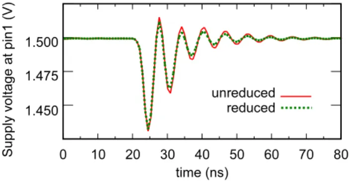
network savings up to 50% for memory and simulation time are achieved. Only very few differences between electrical signals of the reduced model and the original IC conducted emission model exist. The close agreement of a voltage fluctuation at the supply voltage pin during the injection of the time-variant current at the additional pin can be seen in Fig. 7.
8 Conclusions
In this article, an efficient network description of IC con-ducted emission models is presented, which allows for a higher order reduction than the standard description. The proposed description generates a passive network with a smaller number of ports. With standard model order reduc-tion algorithms, such as the block Arnoldi algorithm based on Krylov subspaces, the circuit equations of the network can be reduced. Due to the decreased number of ports a higher order reduction of the proposed network is achieved in com-parison to the standard network. The order reduced equa-tions enable a faster simulation of the frequency-domain be-haviour of the model. With the proposed network synthesis an RC-network including controlled sources of the order re-duced equations can be generated. The synthesised network can further be examined with electrical circuit simulators in time-domain simulations.
The validity of the proposed method is shown with an IC conducted emission model of a 32 Bit microcontroller. A higher order reduction is achieved with the proposed network description as opposed to the standard description. Hereby a higher speed-up factor is achieved, both in the frequency and the time-domain, if the proposed network description is utilised.
Acknowledgements. The authors want to acknowledge A. Reibiger of the Department of Electrical Engineering at the University of Technology Dresden for the useful discussions on network theory and R. Kazemzadeh of the Institute of Electromagnetic Theory at the Leibniz University of Hannover for the discussions on con-ducted emission modelling. The authors want to thank Infineon Technologies AG Germany for providing the IC conducted emis-sion model.
Represented research and development work is carried out in the frame of the MEDEA+ project A701 PARACHUTE project (Par-asitic Extraction and Optimization for Efficient Microelectronic System Design and Application). This particular research was supported by the BMBF (Bundesministerium fuer Bildung und Forschung) Federal Republic of Germany under 01M 3169 A, 01M 3169 D and 01M 3169 E. The responsibility for this publication is held by authors only.
Fig. 7.Voltage at pin1 disturbed by switching currents.
References
Antoulas, A. C.: Approximation of linear dynamical systems, John Wiley and Sons, New York, USA, 1998.
Belevitch, V.: Classical Network Theory, Holden-Day, San Fran-cisco, USA, 1968.
Dhia, S. B., Ramdani, M., and Sicard, E.: Electromagnetic Compat-ibility of Integrated Circuits, Springer, New York, USA, 2006. Feldmann, P.: Model order reduction techniques for linear systems
with large number of terminals, DATE’2004 – Design, Automa-tion and Test in Europe, ExhibiAutoma-tion Conference, Paris, France, 2, 944–947, 2004.
Hellebrandt, S., Zoellin, C. G., Wunderlich, H.-J., Ludwig, S., Coym, T., and Straube, B.: Testing and Monitoring Nanoscale Systems - Challenges and Strategies for Advanced Quality As-surance, International Conference on Microelectronics, Devices and Materials and the Workshop on Electronic Testing, Bled, Slovenia, 3–10, 2007.
Hesidenz, D. and Steinecke, T.: Chip-Package EMI Modeling and Simulation Tool “EXPO”, EMC Compo, Munich, Germany, 2005.
John, W.: Improved EMC Design for Microelectronic Applications, 17th International Wroclaw Symposium and Exhibition on EMC, Wroclaw, Poland, 2004.
Kuh, E. S. and Rohrer, R. A.: Linear Active Networks, Holden-Day, San Francisco, California, USA, 1967.
Odabasioglu, A., Celik, M., and Pileggi, L. T.: PRIMA: Passive Reduced-Order Interconnect Macromodeling Algorithm, IEEE T. Comput. Aid. D., 17(8), 58–65, 1998.
Palenius, T. and Roos, J.: Comparison of Reduced-Order Intercon-nect Macromodels for Time-Domain Simulation, IEEE T. Mi-crow. Theory, 52(9), 2240–2250, 2004.
Radi´c-Weissenfeld, Lj., Ludwig, S., Mathis, W., and John, W.: Model order reduction of linear time-invariant systems, Adv. Ra-dio Sci., in press, 2008.
Silva, J. M. S., Villena, J.F., Flores, P., and Silveira, L.M.: Out-standing Issues in Model Order Reduction, Scientific Computing in Electrical Engineering, Springer, Berlin Heidelberg, Germany, 139–152, 2007.