UNIVERSIDADE DE LISBOA
FACULDADE DE CIˆ
ENCIAS
DEPARTAMENTO DE F´ISICA
Tunnel barrier dielectric breakdown and
endurance in magnetic tunnel junctions
C´
atia Patr´ıcia Santos da Silva
MESTRADO EM F´ISICA
Especializa¸c˜
ao em F´ısica da Mat´
eria Condensada e Nanomateriais
2010
UNIVERSIDADE DE LISBOA
FACULDADE DE CIˆ
ENCIAS
DEPARTAMENTO DE F´ISICA
Tunnel barrier dielectric breakdown and
endurance in magnetic tunnel junctions
Disserta¸
c˜
ao de mestrado orientada por:
Dr. Ricardo Sousa (Spintec)
Dra. Maria Margarida Cruz (FCUL)
C´
atia Patr´ıcia Santos da Silva
MESTRADO EM F´ISICA
Especializa¸c˜
ao em F´ısica da Mat´
eria Condensada e Nanomateriais
2010
Abstract
Magnetic Random Access Memories (MRAM) are starting to replace the cur-rently used RAM memories in specific applications due to non-volatility and fast read and write cycles with no theoretical limitation. To increase its com-petitivity reliability problems need to be overcome. In this work, TA-MRAM cells were studied with specific focus on the problem of degradation induced by the current used in the writing process.
The first part of the work was ramp breakdown tests performed in cells prepared with three different oxidation processes for the MgO tunnel barrier growth.
Two types of breakdown were observed: sharp and progressive. Sharp break-down was found mostly in junctions with plasma oxidized MgO or double oxi-dation process. Progressive breakdown was found to be related to pre-existing pinholes, typically occuring at lower voltage values and associated with low ini-tial TMR and resistance values. The usage of different pulse widths had no significant impact in the observed breakdown type.
The breakdown results of voltage, current density and power density differed greatly with the patterning process, indicating the critical influence of sample processing on the cells’ final behaviour.
The second part of the work consisted in the development of a tester to perform endurance tests and its automatization. Two types of test were made using different intervals: 50 µs and a combination of 50 µs and 75 ns. No indication of increase stress associated with closer pulses was detected.
Three test modes, respecting the injection of the electric current in the cell, were used: positive, negative and alternate. The tested MTJ junctions endure more pulses when they are all negative (negative mode) and the alternative mode causes higher amounts of stress causing breakdown at lower number of applied pulses.
It was observed that application of successive pulses changes the junctions’ magnetoresistive properties, namely the Rmax and coercive field values.
The results found in this work cover a wide range of breakdown parameters and are a contribute to a better understanding of MRAM reliability.
Resumo
A investiga¸c˜ao em mem´orias magn´eticas MRAM ´e actualmente um dos grandes ramos da investiga¸c˜ao em F´ısica e Electr´onica. Estas mem´orias, devido `
a sua n˜ao-volatilidade e capacidade de combinar opera¸c˜oes r´apidas de leitura e de escrita com um n´umero sem limita¸c˜ao te´orica de ciclos de escrita e leitura, s˜ao vistas como potenciais candidatas para substituir, em aplica¸c˜oes espec´ıficas, os tipos de mem´orias usados actualmente.
Um dos maiores obst´aculos no caminho para a industrializa¸c˜ao das MRAM ´
e a ainda insuficiente fiabilidade, pois uma boa mem´oria deve ser capaz de funcionar e guardar a informa¸c˜ao sem falhas por um per´ıodo de 10 anos.
O esquema de escrita termicamente assitido (TA-MRAM) ´e uma evolu¸c˜ao relativamente `a 1ª gera¸c˜ao de MRAM que utiliza a passagem de uma cor-rente el´ectrica atrav´es da jun¸c˜ao de t´unel magn´etica (elemento chave de uma MRAM) para provocar o aquecimento da jun¸c˜ao e reduzir a intensidade do campo necess´ario para a escrita da camada de armazenamento. A passagem da corrente ´e a principal causa da progressiva degrada¸c˜ao da barreira de t´unel tornando-a n˜ao utiliz´avel.
Neste trabalho ´e apresentado um estudo de fiabilidade de mem´orias MRAM. A primeira parte do trabalho consistiu em testes de quebra em jun¸c˜oes com barreiras de t´unel MgO, produzidas atrav´es de diferentes processos de oxida¸c˜ao, por aplica¸c˜ao de impulsos de tens˜ao com valores sucessivamente crescentes – teste de rampa. Foram usados impulsos de 25 e 100 ns, verificando-se que impulsos mais longos causam danos na jun¸c˜ao mais facilmente visto as mesmas quebrarem a valores mais baixos de tens˜ao.
Os diferentes processos de oxida¸c˜ao da barreira MgO est˜ao associados a diferentes tipos de quebra nas amostras analisadas. Jun¸c˜oes oxidadas pelo m´etodo plasma ou com uma dupla camada de MgO apresentam tipicamente um per´ıdo de funcionamento com comportamento constante seguido por uma varia¸c˜ao abrupta de comportamento, com um decr´escimo acentuado de magne-toresistˆencia de t´unel e de resistˆencia, enquanto jun¸c˜oes com a camada de MgO produzida por oxida¸c˜ao natural apresentam um mudan¸ca de comportamento gradual associada `a presen¸ca de defeitos na barreira. Estes dois tipos de que-bra est˜ao associados a mecanismos diferentes de quebra e tipicamente ocorrem em diferentes gamas de tens˜ao, sendo a quebra abrupta aquela que apresenta valores mais elevados de tens˜ao de quebra.
Dois grupos de amostras, com diferentes processos de gravura dos pilares que constituem cada c´elula de mem´oria, foram testados verificando-se que o processo de fabrico tem um papel essencial no comportamento final da mem´oria. Os resultados obtidos para densidade de corrente e de potˆencia variam aproxi-madamente uma ordem de grandeza entre os dois grupos testados.
Numa outra fase do trabalho, foi desenvolvida e automatizada uma mon-tagem experimental para aplica¸c˜ao sucessiva de impulsos. Esta montagem ex-perimental permite o teste de jun¸c˜oes aplicando 106impulsos de tens˜ao atrav´es
das mesmas de modo a caracterizar o seu funcionamento ap´os a aplica¸c˜ao de um n´umero elevado de impulsos.
Dois padr˜oes de envio de impulsos foram usados. Um deles consistiu no envio de impulsos com intervalos de 50 µs entre si enquanto no outro os impulsos eram enviados em grupos de trˆes impulsos espa¸cados entre si de 75 ns e com um espa¸camento de 50 µs entre cada grupo. Foram usados em ambos os casos
impulsos rectangulares com uma largura de 25 ns. A utiliza¸c˜ao destes dois padr˜oes de envio permitiu verificar que, at´e ao limite inferior de 75 ns, n˜ao h´a um aumento significativo dos danos causados `a jun¸c˜ao pela aplica¸c˜ao de impulsos pr´oximos, visto em ambos os casos terem sido obtidos valores semelhantes para o n´umero de impulsos aplicados antes da ocorrˆencia da quebra.
Trˆes tipos de polariza¸c˜ao dos impulsos foram utilizados. Os modos positivo e negativo correspondem `a aplica¸c˜ao de impulsos com polaridade constante ao longo do teste, sendo a polaridade em cada caso definida pelo modo utilizado. No modo alterno os impulsos enviados tˆem alternadamente polaridade negativa e positiva.
Verificou-se que as jun¸c˜oes testadas s˜ao mais resistentes `a aplica¸c˜ao de um maior n´umero de impulsos no modo negativo. Os resultados indicam tamb´em que o modo alterno causa maiores danos `as jun¸c˜oes pois a quebra das mesmas ocorre ap´os a aplica¸c˜ao de um n´umero inferior de impulsos.
Durantes a realiza¸c˜ao destes testes foi verificado que o envio de impulsos de tens˜ao atrav´es das jun¸c˜oes causa mudan¸cas em algumas das suas propriedades magnetoresistivas. Em todos os modos do teste, observou-se que a forma dos ciclos de histerese R(H) varia, tornando-se mais regular ap´os a passagem do primeiro conjunto de impulsos. Verificou-se tamb´em um decr´escimo do valor de resistˆencia m´axima da MTJ, Rmax, com o aumento da amplitude dos
im-pulsos de tens˜ao aplicados, enquanto o valor de resistˆencia m´ınima, Rmin, n˜ao
´
e afectado. Por ´ultimo, observou-se a diminui¸c˜ao do valor do campo coercivo, Hc, com o aumento da tens˜ao, que tende para um valor limite com a aplica¸c˜ao
de tens˜oes mais elevadas. Este ´ultimo efeito tem particular relevˆancia no modo alterno.
Os resultados obtidos neste trabalho cobrem uma vasta gama de parˆametros que influenciam o comportamento de quebra das jun¸c˜oes magn´eticas de efeito de t´unel e s˜ao uma contribui¸c˜ao para uma melhor compreens˜ao dos mecanis-mos envolvidos na degrada¸c˜ao de uma c´elula de mem´oria exposta a diferentes condi¸c˜oes de escrita. A resolu¸c˜ao dos problemas detectados com a consequente melhoria das c´elulas MRAM tornar˜ao estas mem´orias, num futuro pr´oximo, parte do nosso dia-a-dia.
Acknowledgments
The present work was developed in the laboratory Spintec ate Comissariat `
a l’´energie atomique (CEA) in Grenoble under the guidance of Doctor Ricardo Sousa and, later back in Portugal, of Doctor Maria Margarida Cruz. For their time and patience, and specially to Ricardo for accepting me and giving me a chance to work with him, I give them thanks.
For their priceless help in arranging this opportunity, I would like to thank Doctor Guiomar Evans and Doctor Margarida Godinho.
The period of work done in Grenoble was only possible due to the financial help given by CEA and for that I am most grateful.
I would also like to acknowledge everyone at CROCUS Tecnhonologies and the PTA for the warm welcome I was given making me feel comfortable and at home, for all the explanations and, particularly, for the wafers provided to test. Without them this work wouldn’t have been possible.
The life in a completely strange city speaking a strange language can be difficult but it was eased by the friendships made among the people of Spintec, particularly, but not exclusively, among the other trainees working there at the time. Spending time with them, sharing each other’s problems with a certain experimental setup or computer simulation while catching glimpses of other countries and cultures, sharing laughs while at the same time trying to adjust to a common language made the days at Spintec unique. A heart felt thanks and wishes of luck to those friends made along the way.
A person who also became a friend during my stay in Grenoble and who deserves my gratitude is Lucien Lombard, for his patience and help in every step of the way but specially in the beginning and for his companionship. Having to stay late in the lab, trying to figure out what was wrong with the VEECO, was a little less frustrating when he was around.
To my portuguese friends, who never let me feel lonely or abandoned by them, even though we were thousands of quilometers away from each other, to family, specially my parents, who supported me in this six months of absence and have supported me my entire life making all this possible, and to my boyfriend, Tiago Santos, who not only kept supporting me while I was away but was also very important in the writing of this report, hearing my complaints, reading it, making comments and giving priceless help whenever I was stuck, I leave my most special thanks. Thank you, to all of you, for being a part of my life.
Agradecimentos
O trabalho apresentado foi desenvolvido no laborat´orio Spintec pertencente ao Comissariat `a l’´energie atomique (CEA) em Grenoble sob a supervis˜ao do Doutor Ricardo Sousa e, mais tarde em Portugal, da Doutora Maria Margarida Cruz. Pelo seu tempo e paciˆencia, e em especial ao Ricardo por me ter aceite e dado a oportunidade de trabalhar com ele, eu agrada¸co-lhes.
Pela sua ajuda preciosa na prepara¸c˜ao desta oportunidade, eu gostaria de agradecer `a Doutora Guiomar Evans e `a Doutora Margarida Godinho.
O per´ıodo de trabalho em Grenoble apenas foi poss´ıvel devido `a ajuda fi-nanceira fornecida pelo CEA e pelo qual estou muito grata.
Gostaria de agradecer a toda a gente da CROCUS Technologies e da PTA pelo caloroso acolhimento que me fez sentir confort´avel e em casa, por todas as explica¸c˜oes e, particularmente, pelos conjuntos de amostras fornecidos para testar. Sem eles este trabalho n˜ao teria sido poss´ıvel.
A vida numa cidade estranha a falar uma l´ıngua estranha pode ser d´ıficil mas a estadia foi facilitada pelas amizades feitas entre as pessoas da Spintec, partic-ularmente, mas n˜ao em exclusivo, entre os outros estagi´arios que l´a trabalharam no mesmo per´ıodo. Passar tempo com eles, partilhar problemas com alguma montagem experimental ou simula¸c˜ao, conhecer fragmentos soltos de outras cul-turas e hist´orias de outros pa´ıses, partilhar gargalhadas enquanto tent´avamos adaptar-nos a uma l´ıngua comum fez com que os dias passados na Spintec sejam ´
unicos. Um caloroso agradecimento e desejos de sorte para esses amigos feitos pelo caminho.
Uma pessoa que tamb´em se tornou um amigo durante a minha estadia na Spintec e que merece a minha gratid˜ao ´e o Lucien Lombard, pela sua paciˆencia e ajuda ao longo de todo o percurso mas especialmento no in´ıcio e pelo seu companheirismo. Ter de ficar at´e tarde no laborat´orio, a tentar perceber o que se passaria com o VEECO, era um bocadinho menos frustrante quando ele estava por perto.
Ao meus amigos em Portugal, que nunca me deixaram sentir sozinha ou abandonada por eles mesmo havendo milhares de quil´ometros entre n´os, `a minha fam´ılia, especialmente aos meus pais, que me apoiaram nesta ausˆencia de seis meses e sempre me apoiaram toda a vida, e ao meu namorado, Tiago Santos,que n˜ao s´o me apoiou enquanto estive longe mas tamb´em foi muito importante na escrita desta tese, ouvindo as minhas queixas, lendo-o, fazendo coment´arios e dando um precioso empurr˜ao sempre ficava encalhada, deixo o meu obrigada mais especial. Muito obrigada, a todos v´os, por fazerem parte da minha vida.
Contents
1 Introduction 1
1.1 Magnetic Tunnel Junction and Tunnel Magnetoresistance . . . . 1
1.2 First generation of MRAM . . . 4
1.3 Thermally Assisted MRAM . . . 4
1.4 Spin Torque Transfer MRAM . . . 7
2 Experimental details 8 2.1 Sample fabrication . . . 8
2.2 Fabrication problems . . . 10
2.3 Quasi-static test . . . 11
2.4 Ramp breakdown test . . . 12
2.5 Endurance breakdown test . . . 13
3 50 mm wafers - Spintec process 17 3.1 Sample description . . . 17
3.2 Initial mapping . . . 20
3.3 Breakdown results . . . 24
3.4 Summary . . . 31
4 200 mm wafers - CROCUS process 32 4.1 Sample description . . . 32
4.2 Initial mapping . . . 33
4.3 Breakdown results . . . 34
4.4 Summary . . . 40
5 Endurance in Magnetic Tunnel Junctions 41 5.1 Endurance test results . . . 41
5.2 Magnetoresistive properties . . . 44
5.3 Summary . . . 47
6 Conclusion 48
A Programming of the New Tester 50
List of Figures
1.1 Schematic of the three layers that compose a magnetic tunnel junction (MTJ). . . 2 1.2 Representation of the dependence of the conductance with the
orientation of spin. Both parallel (left) and anti-parallel (right) configurations are represented. . . 3 1.3 Hysteresis cycle obtained when a magnetic field acts on a
mag-netic tunnel junction. . . 3 1.4 Desing of the first generation of MRAM cells [1]. . . 5 1.5 Representation of the key layers that compose a memory cell of
a TA-MRAM. . . 5 1.6 Hysteresis cycles obtained in the different steps of the writing
process. On the left, we can se the cycle before the process, in the middle we have the cycle obtained just after the current passed through the junction, heating it and breaking the coupling between the storage layer and the antiferromagnet, and to the right is the final cycle, obtained by letting the junction cool with applied field. . . 6 1.7 Schematic of the three layers that compose a synthetic
antiferro-magnet. . . 6 1.8 Representation of the layers of a TA-MRAM cell. . . 6 2.1 Schematic representation of the current-in-plane tunneling method. 9 2.2 Schematic of the magnetic momenta in a ferromagnetic and
an-tiferromagnetic layers during the process of alignment. . . 10 2.3 Representation the lines of current in the presence of a pinhole
in the insulating barrier . . . 10 2.4 Simple schematic representation of the three resistances - MTJ,
Rserial and shunt - and graphical representation of the effect of
each resistance. The line corresponding to a shows the effect of a serial resistance, b corresponds to the effect of shunt and, finally, c corresponds to the effect of change in nominal diameter. . . 11 2.5 Photo (left) and schematic [16] (right) of the QSW tester. . . 12 2.6 Detail of the probe card used to perform the mapping of a wafer.
The configuration of the probes is designed to match the design of the pads it is supposed to make contact with. . . 13
2.7 Example of hysteresis cycles obtained during a breakdown test performed with the QSW tester (left): The pulses are applied at the position indicated in the figure during the first cycle (blue). The second cycle (red) checks the condition of the junction, and in this case we see that it remained functional. Schematic repre-sentation of the pulses applied during the ramp test (right). . . . 14 2.8 Photos of the new tester. The coil system responsible for the field
and the RF probe are visible to the right. . . 14 2.9 Schematic of the setup used in the early stages of development of
the tester. . . 15 2.10 Schematic of the final setup of the new tester. Thicker lines
correspond to GPIB connections. In the upper left corner we can see a representation of the RF probe used. . . 16 2.11 Representation of the pulses sent through the junction in both
types of test done with the new tester. . . 16 3.1 Representation of the distribution of dies in a 50 mm wafer. . . . 18 3.2 In each region of the wafer there are different types of chips,
however only the ones represented above are measured. The red lines on the chips correspond to a top lines and the yellow lines correspond to bottom lines. The junctions can be found in the middle of the chips at the intersections between the lines coming from the pads and the common lines. . . 18 3.3 Distribution of TMR in wafers processed with simple natural
ox-idation, P475 (left) and P488 (right). The different lines corre-spond to different junction sizes. . . 21 3.4 Distribution of TMR in wafer processed with plasma oxidation,
P515. The different lines correspond to different junction sizes. . 21 3.5 Distribution of TMR in wafers with double layer of MgO, P480
(left) and P487 (right). The different lines correspond to different junction sizes. . . 21 3.6 TMR as a function of Rmax for for wafers P475 (left) and P488
(right) - natural oxidation. . . 22 3.7 TMR as a function of Rmaxfor wafer P515 - plasma oxidation. . 22
3.8 TMR as a function of Rmax for wafers P480 (left) and P487
(right) - double layer of MgO. . . 22 3.9 Typical breakdown of a junction from a wafer with natural
oxida-tion of the MgO layer (top), plasma assisted oxidaoxida-tion (middle) and double oxidation (bottom). The inset of each plot shows the change in TMR with the application of the pulses. . . 25 3.10 Breakdown voltage results for junctions with a diameter of 500
nm (left) and 100 nm (right). . . 26 3.11 Results of power density at breakdown point for junctions with
a diameter of 500 nm (left) and 100 nm (right). . . 27 3.12 Results of current density at breakdown point for junctions with
a diameter of 500 nm (left) and 100 nm (right). . . 27 3.13 Representation of two different currents flowing through a
mem-ory cell in opposite directions, showing the definitions of positive and negative current. . . 29
3.14 Comparison of voltage breakdown results obatined with the cur-rent flowing in ascending and descending directions for dots of 100 nm of diameter of both wafers with naturally oxidized MgO, P475 (left) and (P488). . . 29 3.15 Comparison of voltage breakdown results obatined with the
cur-rent flowing in ascending and descending directions for dots of 100 nm of diameter of wafer P515 (plasma oxidation). . . 30 3.16 Comparison of voltage breakdown results obatined with the
cur-rent flowing in ascending and descending directions for dots of 100 nm of diameter of both wafers with double oxidation, P480 (left) and P487 (right). . . 30 4.1 Photo of a 200 mm wafer placed on the chuck responsible for its
movement in the QSW tester. . . 32 4.2 Breakdown voltage with 25 and 100 ns pulses for the wafer with
plasma oxidation (left) and double oxidation (right). . . 34 4.3 Comparison of breakdown voltage results between wafers the two
wafers: SL33 (plasma oxidation) and FL2 (double oxidation). Results concern both the test using 25 ns (left) and 100 ns pulses (right). . . 35 4.4 Comparison of breakdown current density results between wafers
the two wafers: SL33 (plasma oxidation) and FL2 (double layer of MgO). Results concern both the test using 25 ns (left) and 100 ns pulses (right). . . 35 4.5 Comparison of breakdown power density results between wafers
the two wafers: SL33 (plasma oxidation) and FL2 (double layer of MgO). Results concern both the test using 25 ns (left) and 100 ns pulses (right). . . 36 4.6 Breakdown voltage results for wafer SL33 (plasma oxidation)
sorted by the direction of the current flowing through the junction. 36 4.7 Breakdown voltage results for wafer FL2 (double oxidation) sorted
by the direction of the current flowing through the junction. . . . 37 4.8 Comparison of results of breakdown voltage for both sharp and
progressive breakdown. Results for wafer SL33 (plasma oxida-tion) are presented in the left and results from wafer FL2 (double oxidation) to the right. . . 38 4.9 Comparison of results of initial Rminfor both sharp and
progres-sive breakdown. Results for wafer SL33 (plasma oxidation) are presented in the left and results from wafer FL2 (double oxida-tion) to the right. . . 38 4.10 Comparison of results of initial TMR for both sharp and
progres-sive breakdown. Results for wafer SL33 (plasma oxidation) are presented in the left and results from wafer FL2 (double oxidatito the right. . . 39 5.1 Schematic of the flow of the current through the pillar for both
positive (left) and negative (right) modes. . . 41 5.2 Comparison of results obtained for the pulses until breakdown
5.3 Comparison of results obtained for the pulses until breakdown for each mode of voltage application using the second type of test. 43 5.4 Comparison of the results obtained in each type of test, defined
in the legends as 50 µs and 75 ns, for each mode used - alternative (top), negative (bottom left) and positive mode (bottom right). . 43 5.5 Examples of the change of shape of the hysteresis cycles after the
application of voltage pulses through the junction. . . 44 5.6 Hysteresis cycles of a junction measured with the application of
different values of voltage, showing a decrease in Rmaxand TMR
with the increase of the voltage applied. . . 45 5.7 Hysteresis cycles showing the change of coercive field with the
List of Tables
3.1 Nominal sizes of each type of dot present in a 50 mm wafer. . . . 17 3.2 Extension of diameter and serial resistance values for each size
and each analysed wafer. . . 23 3.3 Expected and estimated RA values for each wafer. . . 24 3.4 Statistics of the breakdown behaviour observed on circular dots
for each of the tested wafers. . . 25 3.5 Mean values of breakdown voltage, current density and power
density for the 100 nm dots of each wafer. . . 28 3.6 Mean values of breakdown voltage, current density and power
density for the 500 nm dots of each wafer. . . 28 3.7 Statistics of breakdown type for the eliptical dots (100×50 and
140×40) of each wafer. . . 29 4.1 Results obtained by current in plane TMR measurement (CAPRES
tool). . . 33 4.2 Results of diameter extension and serial resistance obtained from
the mapping of the wafers. . . 33 4.3 Breakdown results for wafers SL33 (plasma oxidation) and FL2
(double oxidation), for both pulse widths used in the tests. . . . 34 4.4 Breakdown type statistics for wafers SL33 and FL2. . . 37
Chapter 1
Introduction
Presently, most of our computers use silicon-based devices to temporarily store the information necessary for the microprocessor’s operations. These devices, mostly Static Random Access Memories (SRAM) and Dynamic Random Access Memories (DRAM), allow a fast access to information but rely on electrical power to sustain the data, which means that all information is lost as the power is switched off.
FLASH memories are non-volatile memories used typically in USB pen drives and cell phones, but they are limited in the number of write cycles they can perform, typically 104− 106.
A new concept of memory, that combines non-volatility, low power consump-tion and fast read and write cycles with no theoretical limitaconsump-tion, is emerging. These new memories, that integrate a magnetoresistive device with a silicon-based selection matrix, are called Magnetic Random Access Memories (MRAM). The properties of these devices make them potential alternatives to the currently used memory types in specific applications [1].
1.1
Magnetic Tunnel Junction and Tunnel
Mag-netoresistance
The key element in the design of the MRAM is a three layer system of two fer-romagnetic layers separated by a thin insulating layer, whose thickness typically ranges from a few angstroms to 3-4 nanometers. Current flowing perpendicular to the layers, crosses the insulator by tunneling effect with an intensity that depends on the relative orientation of the magnetization of the ferromagnetic layers, giving rise to tunnel magnetoresistance (TMR). The group of three layers is called a magnetic tunnel junction (fig. 1.1).
The explanation of the TMR relies on the assumption of Mott’s two cur-rent model [2] that assumes that electrons with diffecur-rent spin are associated with independent conduction channels. As the electrons flow through the first ferromagnetic layer, the current becomes spin polarised due to the interaction with the magnetization of the layer, and the two currents are not equivalent. A model was proposed by Julliere [3], based on the experimental results of Tedrow and Meservey [4], that assumes that the spin of the electrons is maintained
Figure 1.1: Schematic of the three layers that compose a magnetic tunnel junc-tion (MTJ).
during tunnelling and electron current flow for different spin orientations occurs through independent channels.
The probability of transition by tunnel effect of an electron from one ferro-magnetic layer to the other is proportional to the product of the initial density of states, n1, in the first ferromagnetic layer and the final density of states, n2,
in the second ferromagnetic layer wheighted by the probability of transition, T, across the barrier and, consequently, the conductance current has the same dependence. I(V ) ∝ Z +∞ −∞ |T (E)|2n 1(E − eV )n2(E − eV )[f (E − eV ) − f (E)]dE (1.1)
where f(E) represents the Fermi distribution. Julliere considered that the tran-sition probability is independent of energy and only electrons in the Fermi level contribute. For the two cases where the ferromagnetic layers magnetizations are parallel or anti-parallel (P or AP), the electron conductance is proportional to the product of the density of states in the two layers for the two channels.
GP ∝ n↑1.n ↑ 2+ n ↓ 1.n ↓ 2 GAP ∝ n↑1.n ↓ 2+ n ↓ 1.n ↑ 2 (1.2)
where 1 and 2 are the indexes of both layers and n↑ and n↓ are the density of states at the Fermi level of spin up and down, respectively. The tunnel probability is higher in the case of parallel alignment, when the majority spin directions of the initial electrode corresponds to that in the final electrode. The higher conductance G results in a lower resistance of the tunnel junction. Therefore, a change in the magnetic configuration of the layers, will also change the current flow through the junction (fig. 1.2).
Julliere determined a simple formula for the tunnel magnetoresistance
T M R = GP− GAP GAP
=RAP− RP RP
(1.3) where RP and RAP are the resistances of the junction in the parallel and
anti-parallel states, respectively.
The change of resistance with the magnetic layer configuration is what allows this system to function as a memory. The different configurations, P and AP, can be assigned to logical values of “0”and “1”(fig. 1.3).
Figure 1.2: Representation of the dependence of the conductance with the ori-entation of spin. Both parallel (left) and anti-parallel (right) configurations are represented.
Figure 1.3: Hysteresis cycle obtained when a magnetic field acts on a magnetic tunnel junction.
In order to have only the magnetization reversal of a single layer, the storage layer, it is necessary to fix the magnetization direction of the second layer used as a reference layer. An antiferromagnetic layer below or on top of the reference ferromagnetic layer is used for that purpose. The antiferromagnet produces an exchange bias that shifts the hysteresis loop of the reference layer, causing its magnetization to remain stable in a field range around zero. The ferromagnetic layer whose magnetization is fixed is then called reference layer. The logical values “0”and “1”are identified by comparing the resistance value obtained at zero field and comparing it with a reference value between RAP and RP, which
will be designated henceforth as Rmaxand Rmin, respectively.
The research in this type of memories gained considerable interest when in 1995 for the first time TMR was observed at room temperature. TMR of the order of 12% was observed with a junction having aluminium oxide (Al2O3) as
the tunnel barrier [5]. For several years, amorphous alumina remained the most commonly used tunnel barrier in the fabrication of MRAM cells, obtaining about 70% TMR with CoFeB as electrodes [6]. However the theoretical prediction of a TMR of the order of 1000% using epitaxial barrier of MgO [7, 8] led most research groups to pursue their investigations using MgO instead of alumina as the tunnel barrier.
1.2
First generation of MRAM
In the first generation of MRAM cells, the reversal of the storage layer was carried out using a magnetic field. To change only one of the cells each time, the critical value was achieved adding two magnetic fields induced by two currents passing through two lines above and below the junction (fig. 1.4).
The usage of two current lines allowed the correct addressing of the dot to write. However, as the density of dots increases to allow the storage of greater volumes of data, the writing process starts to induce errors in neighboring cells. Another problem is the fact that this design leads to great power consumption due to the necessity of having two fields applied simultaneously.
1.3
Thermally Assisted MRAM
Another design, proposed recently by the laboratory Spintec [1], uses a second antiferromagnet to exchange bias the storage layer, and flow of current through the junction to increase temperature and unblock the storage layer for writing the cell using lower fields. This type of memory cell, called Thermally Assisted MRAM (TA-MRAM) (fig. 1.5), presents several advantages. The indexing of the dots, during the writing, is more accurate since it results from the combination of field and current flowing through the junction to write it (fig. 1.6). This means that only one field line is needed in the writing process and the necessary field values are lower, which decreases the power consumption.
The antiferromagnet on top of the storage layer creates an additional ex-change field that reduces the chances of a stray field being capable of changing the data in non addressed cells since that field would have to be larger than the sum of the coercive field, Hc, and the exchange field, Hexch[1]. This means that
Figure 1.4: Desing of the first generation of MRAM cells [1].
Figure 1.5: Representation of the key layers that compose a memory cell of a TA-MRAM.
In order to reduce the stray field created by the patterned reference layer on the storage layer a synthetic antiferromagnet (SAF) is used in the reference layer. A SAF (fig. 1.7) is a tri-layer system composed by two ferromagnetic layers and a thin spacer between them. The interlayer coupling of the type RKKY (Ruderman-Kittel-Kasuya-Yosida) interaction between the two ferromagnetic layers can lead to a parallel or anti-parallel alignment of the magnetization of the two layers depending on the thickness of the spacer.
Choosing the thickness of the spacer properly to obtain an anti-parallel con-figuration and two non identical ferromagnetic layers it is possible to have a compensation of the stray fields generated by the two SAF ferromagnetic layers in the region of the storage layer. Typically the ferromagnetic layers used in the SAF are CoFeB and CoFe and the spacer is Ru with 0.8 nm.
The TA-MRAM presents several advantages compared with other concepts. However, the need of a current flow through the junction in the writing process
Figure 1.6: Hysteresis cycles obtained in the different steps of the writing pro-cess. On the left, we can se the cycle before the process, in the middle we have the cycle obtained just after the current passed through the junction, heating it and breaking the coupling between the storage layer and the antiferromagnet, and to the right is the final cycle, obtained by letting the junction cool with applied field.
Figure 1.7: Schematic of the three layers that compose a synthetic antiferro-magnet.
causes stress to the tunnel barrier and can accelerate degradation. With the ap-plication of high voltage pulses, pinholes can be created, rendering the memory cell useless. Since a good memory needs to be read and written a great number of times, this means that reliability is a problem of great importance for these devices. A study of their reliability can help develop better memory cells that will, in time, make their way into our own computers [9, 10].
1.4
Spin Torque Transfer MRAM
Another generation of MRAM has a writing scheme in which a spin polarised current is responsible for the reversal of the storage layer using spin torque transfer. This design, called Spin Torque Transfer MRAM (STT-MRAM), has the advantage of eliminating the need for a field line thus greatly reducing the power consumption when compared with other designs. The structure of the memory cells is similar to the one presented in figure 1.5, except that no antiferromagnet is used to exchange bias the storage layer.
The writing of a bit is done by passing a sufficiently strong current through the junction and the flow direction depending on the state to write. To write a “0”, the parallel state, the current flows from the reference layer to the storage layer and it flows in the opposite direction to write a “1”, which corresponds to the anti-parallel state.
Due to the need of ensuring a stability of the data of the order of 10 years, a constraint in the reduction of size of this memory cells was found. The limit in the reduction of the size using this design has led researchers to pursue research using new configurations. At the moment, a combination of this design with the one of TA-MRAM, using of an antiferromagnet to exchange bias the storage layer, and the usage of materials with perpendicular magnetization are configurations under test.
Chapter 2
Experimental details
2.1
Sample fabrication
The memory cells tested in this work were deposited by sputtering on a SiO2
substrate. Each of the deposited layers has a specific role in the pillar, and the main parts, in order of deposition, are:
Buffer.
Antiferromagnet whose function is to exchange bias the reference layer. Synthetic antiferromagnet, in which the reference layer is included. Tunnel barrier.
Storage layer.
Antiferromagnet that couples with the storage layer. Capping.
Etch stop layer. Top electrode
After the deposition process is complete, the wafer is totally covered by the deposited materials and has the appearence of a mirror. At this point a tunnel magnetoresistance measurement on a CAPRES tool can be carried out. In this current-in-plane tunneling method, four small probes are place colinearly on the surface of the wafer with a given spacing x (fig. 2.1). Current is sent through two of the probes (labelled I+ and I-) and the voltage drop between the other
two probes is measured (V+ and V-). The distance x between the probes is of vital importance since if the probes are very close together all the current flows through the top electrode but in the case of wide spacing the current will be proportionally divided between the top and bottom electrodes. Measurements are carried out using several different spacings and the data is then fitted to theory using TMR, RA, RT and RB as parameters [11], where RT and RB
Figure 2.1: Schematic representation of the current-in-plane tunneling method.
for an accurate measurement of the RA and maximum TMR without artifacts originating from the processing steps [12].
Two different processes were used to pattern the wafers tested in this study. However, since the the fabrication of the samples was outside the scope of my work, only a brief general description of the processes will be presented given that I am unfamiliar with the details of the processes.
The wafers to be patterned are covered with a resinous material and, in the areas where the pillars will be, holes are made using electrom beam lithography until a depth of 20 nm below the resin layer is achieved. A layer of platinum is then deposited to cover the area of the top of the pillar to be patterned and the resin is chemically removed.
Reactive-Ion Etching (RIE) is used to pattern the region of the top electrode, with the platinum serving as a hard mask for the pillars. This process uses a reactive plasma, typically Cl- or F-, to react with the tantalum of the top electrode layer. Secondary ion mass spectrometry (SIMS) is used to identify the expelled ions to control que progress of the etch. When elements of the etch top layer, typically IrMn, start to be found by SIMS the RIE is terminated. This etching process allows a fast patterning of the region composed of tantalum because the reactive gases used react very fast with it and slowly with the IrMn of the etch stop layer, preventing the etch to etch further than desired.
RIE can’t be used at the level of the magnetic stack because it would damage the MTJ and compromise the memory cell therefore, after this level and until the tunnel barrier is reached, the patterning process is continued using Ion-Beam Etch (IBE). This process works using the same principle as sputtering. Ions are accelerated into the wafer with a defined angle causing the removal of deposited matter and progressively giving shape to rest of the pillar. As before, SIMS is used to detect when the tunnel barrier is reached so that the process is stopped.
At this point, the pillars are completely formed. The next step is the creation of the contacts. In the final part of the process, a set of masks is used to make the necessary depositions of metal and oxides so that there are metal connections only in the desired regions.
After the processing of the wafer, which is a process that takes aproximately two weeks, and before the devices are usable, it is necessary to align all the refer-ence layers in the same direction by annealing, to a temperature above the N´eel temperatures of the two antiferromagnets and below the Curie temperature of the reference layer, and letting the cells cool down in an applied field (fig. 2.2).It is very important that the antiferromagnet used to couple with the reference
Figure 2.2: Schematic of the magnetic momenta in a ferromagnetic and antifer-romagnetic layers during the process of alignment.
Figure 2.3: Representation the lines of current in the presence of a pinhole in the insulating barrier
layer has a higher N´eel temperature than the one coupled with the storage layer, so that when the junction is heated the exchange coupling between the antifer-romagnet and the reference layer is not broken and the magnetization of the reference layer can remain stable. The annealing stage is a crucial step in the development of a wafer. The conditions used, such as temperature and dura-tion, can lead to memory cells of good behaviour or to a great decrease in TMR and produce memory cells that are not usable [13, 14].
After all this steps are complete, the devices are finally ready to be tested or, in the case of a working memory, to be used.
2.2
Fabrication problems
The fabrication of the tunnel barrier, and also the pillar fabrication are critical for the final device. Several problems can occur during deposition and processing that cause the memory cell not to function properly. A particularly serious problem is the formation of pinholes in the barrier. A pinhole (fig. 2.3) is a region of the insulating layer where its thickness is so reduced that a short-circuit is created between the two electrodes. If, for example, the layer where the tunnel barrier is to be deposited is too rough, the irregular surface may lead to the creation of pinholes [15]. Another possible cause for the formation of pinholes is a change in lattice parameter while the Mg is oxidized to obtain MgO. Further discussion on this cause is present in the following chapters.
The process used to pattern the pillars, to build the memory cells, as de-scribed above, requires the use of Ion Beam Etch (IBE). During this phase of
Figure 2.4: Simple schematic representation of the three resistances - MTJ, Rserialand shunt - and graphical representation of the effect of each resistance.
The line corresponding to a shows the effect of a serial resistance, b corresponds to the effect of shunt and, finally, c corresponds to the effect of change in nominal diameter.
the process ions are accelerated into the wafer with a defined angle to progres-sively give shape to the pillars. However, due to the angle of the beam, a part of the removed matter is re-deposited on the walls of the pillars, which acts as a resistance in parallel with the MTJ. The re-deposition on the side walls creates a path for the current, therefore reducing the resistance of the junction and degrading its TMR. The angle used is also responsible for the creation of a “shadow”around the pillar in the engraving process where the matter is not removed. Consequently the dots obtained after patterning will have a diameter larger than the nominal value, the difference being designated by extension.
dreal= dnominal+ extension (2.1)
Another effect that also degrades the TMR of the junction is the serial resistance, associated with contacts and interfaces, which causes an increase of the resistance of the junction but doesn’t contribute to its TMR. A simple model of the three resistances involved - the junction, the serial resistance and the shunt created by the re-deposition - and their effects in the value of TMR are presented in fig. 2.4.
2.3
Quasi-static test
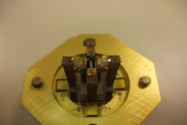
The work done during my training at Spintec can be divided into two parts. In the first part, a Quasi-Static Wafer (QSW) tester was used (fig. 2.5). This experimental setup is a fully automated test system for characterizing the mag-netoresistance of bulk films and patterned devices by performing measurements of resistance while an applied field is varied within a defined range. The tester offers the possibility of performing the measurements using constant voltage or
Figure 2.5: Photo (left) and schematic [16] (right) of the QSW tester.
constant current. In this case, the tests were performed applying a low con-stant voltage, of the order of 100 mV, to the contacts of the junction and the produced current was measured to obtain the value of resistance, using a four point configuration. A probe card (fig. 2.6), with the desing of the contacts of each junction, was used to make the contacts. The program of the tester was configured to perform the correct addressing of current and voltage to the dif-ferent probes in order to perform the measurement. A system of coils, located close to the sample, was responsible for the production of a magnetic field in the same plane of the wafers. Typically, the field ranged from -1000 to 1000 Oe. The quasi-static test, also called R(H) measurement, allows the mapping of the wafers, providing information about the distribution of TMR and resistance and also the values of Rserial and the enlargement of each measured dot type
compared to the nominal dot diameter.
2.4
Ramp breakdown test
Introducing a switch, a bias-T and a pulse generator in the previous setup and replacing the probe card by a similar one with RF probes we can send voltage pulses through the MTJ. The bias-T allows to add high frequency short width pulses to the DC bias current used for the quasi-static R(H) measurement. The tester controls the R(H) measurement, while the pulse generator is responsible for sending the pulses that will cause heat and stress in the junction. The switch is controlled by the tester to connect the junction either to the tester for a R(H)
Figure 2.6: Detail of the probe card used to perform the mapping of a wafer. The configuration of the probes is designed to match the design of the pads it is supposed to make contact with.
measurement or to both the pulse generator and the tester so that we can have both applied field and application of a pulse (fig. 2.5).
The purpose of this setup in my work was to perform a ramp breakdown test. This test consists in the application of pulses through the junction with increasing amplitude, at a given value of applied field during an hysteresis cycle (fig. 2.7). After the application of each pulse, a field sweep is performed and the resistance of the junction is measured to determine whether or not it is broken. If it is broken, the tester proceeds to the next junction. If not, the amplitude of the pulse is increased and the test is repeated until breakdown occurs. The typical pulse widths used were 25 and 100 ns. Using different pulse widths we can study their influence on the breakdown behaviour [16].
2.5
Endurance breakdown test
The second part of my work consisted in assembling a new tester (fig. 2.8) and writing the control programs (see appendix A) using Matlab that allowed the performance of endurance tests.
In the first steps of development the basic instruments that would become part of the final setup were used to perform simple R(H) measurements accessing only front panel operations. This allowed to identify and choose the commands necessary to do the measurement and obtain the corresponding information. These commands became the base of the control program.
At this point, no pulse generator was used and the measurements were car-ried out with two independent probes. A representation of the tester in this phase of the development can be seen in fig. 2.9.
The second phase of the development consisted in establishing communi-cation between all the instruments via GPIB control and introducing a pulse generator to the setup. A bias-T was used in order to superimpose the signal
Figure 2.7: Example of hysteresis cycles obtained during a breakdown test per-formed with the QSW tester (left): The pulses are applied at the position indicated in the figure during the first cycle (blue). The second cycle (red) checks the condition of the junction, and in this case we see that it remained functional. Schematic representation of the pulses applied during the ramp test (right).
Figure 2.8: Photos of the new tester. The coil system responsible for the field and the RF probe are visible to the right.
Figure 2.9: Schematic of the setup used in the early stages of development of the tester.
used to measure the resistance of the junction and the pulses sent by the pulse generator. When pulses were applied, an RF probe with 40GHz bandwidth was used to contact the junction (fig. 2.10).
Unlike what was done in the QSW tester, the tests performed using this new tester were carried out using a constant current and measuring the resulting voltage at the contacts of the junction. The value of current used was calculated for each junction so that the voltage obtained was aproximately of the order of 100 mV. This procedure ensured that no junction was broken due to the current used for the measurement.
A system of four coils was used to produce a field in the plane of the samples (fig. 2.8). The amplitude of the field was determined by the amplitude of the voltage sent by the wave generator to the current source connected to the coils. Using a sample measured in a known field it was possible to convert the voltage applied to the current source into the resulting magnetic field value. For this tester the convertion is of 45 Oe per volt. The tests were carried out using a triangular wave with an amplitude of 9 V and a frequency of 5 Hz, which corresponds to a magnetic field varying with the same frequency and ranging from -405 to 405 Oe.
The purpose of the tests designed to be performed with this tester was to check the endurance of the junctions to 106 consecutive applied pulses. In this tests, the pulses were sent throughout the entire range of magnetic field available with defined intervals between them.
The pulses were applied in three different modes (fig. 2.11): Positive mode - All the pulses sent positive amplitude. Negative mode - All the pulses sent negative amplitude.
Alternate mode - Consecutive pulses have different polarities, alternating between positive and negative.
Figure 2.10: Schematic of the final setup of the new tester. Thicker lines corre-spond to GPIB connections. In the upper left corner we can see a representation of the RF probe used.
Using these different tests we can see if the direction of the current has an effect in its breakdown behaviour [17, 18].
Initially, the pulses were applied with an interval of 50 µs, allowing the junction to have enough time to return to room temperature and no cumulative heating effects were expected. In this configuration, we can consider the pulses as independent.
In a second test the sequence of pulses was changed to groups of three pulses, with an interval of 75 ns between them, followed by an interval of approximately 50 µs (fig. 2.11), in order to verify if closer pulses would cause the junctions to present different breakdown behaviour.
The results obtained in all the tests performed and the respective discussion are presented in the following chapters.
Figure 2.11: Representation of the pulses sent through the junction in both types of test done with the new tester.
Chapter 3
50 mm wafers - Spintec
process
3.1
Sample description
The first wafers used were 50 mm wafers deposited by CROCUS Technologies and processed at the PTA1.
The structure of these wafers is represented in fig. 3.1. Each letter corre-sponds to two possible types of dots, as they are divided in two groups typically designated by top and bottom due to the placing of the common line that con-nects the five junctions present in each chip. In fig. 3.2 we can see two rows of chips and we can easily distinguish between top and bottom chips using the arrow (^) next to the number imprinted on the chip that corresponds to chips top. The junctions can be found in the middle of the chips at the intersections between the lines coming from the pads and the common lines. Different letters typically correspond to different sizes. The sizes associated with each dot type can be found in table 3.1. Both circular and elliptical dots are present in the wafers.
Structure type Nominal size (nm×nm)
A top 500×500 bottom 100×100 E1 top 140×40 bottom 100×100 E top 100×50 bottom 50×50
Table 3.1: Nominal sizes of each type of dot present in a 50 mm wafer.
The interest of the wafers tested resides mostly in the fact that the oxidation process to obtain the MgO tunnel barrier differs from wafer to wafer. Apart
1PTA, Plateforme Tecnologique Avanc´e, is a class 1000 clean room, that extends over
350m2in building 10.05 in CEA, Grenoble. It is used by several laboratories such as CNRS,
Figure 3.1: Representation of the distribution of dies in a 50 mm wafer.
Figure 3.2: In each region of the wafer there are different types of chips, however only the ones represented above are measured. The red lines on the chips correspond to a top lines and the yellow lines correspond to bottom lines. The junctions can be found in the middle of the chips at the intersections between the lines coming from the pads and the common lines.
from that difference, the rest of the magnetic stack is the same. Five wafers were tested for breakdown, corresponding to three different tunnel barrier fabrication processes.
1. The process most commonly used to obtain an MgO layer is plasma assisted oxidation of an Mg layer. This process allows the oxidation step to be fast and achieves an oxidation deep in the Mg layer.
2. Natural oxidation, i.e. the oxidation achieved naturally due to the oxygen atmosphere in the deposition chamber, was another process used. This is a much slower process that leads to a more superficial oxidation. 3. The third process used consists in performing the oxidation of the Mg in
two oxidation steps. Initially, a first thin Mg layer is deposited and natu-rally oxidized. After this step is complete, a second Mg layer is deposited on top of the previous one and another natural oxidation is performed. This process is designated in this report as double oxidation.
In both plasma and simple natural oxidation processes, described above, the MgO layer is obtained by oxidizing a single Mg layer. Since the lattice parame-ters of Mg and MgO are not the same, the oxidation phase leads to a change in the lattice and can lead to the creation of pinholes (see chapter 1) in the tunnel barrier compromising the electrical characteristics of the junction. A pinhole dilutes the TMR, since most of the current flowing through the pillar will pass through it instead of through the MgO tunnel barrier. The existence of pinholes can also cause a junction to be more susceptible to progressive breakdown [19], since a small pinhole tends to become larger with the flow of current through the junction.
The third process described was designed to minimize the creation of pin-holes in the tunnel barrier during the oxidation step. The probability of having pinholes in each MgO layer is the same as with simple natural oxidation, how-ever the probability of having two pinholes in the MgO layers that are vertically aligned is much smaller. This process achieves an RA product2 that is
approx-imately the sum of the RA product of the two deposited layers. The expected and estimated RA values for each wafer are presented in table 3.3.
Each wafer has a designation, given during deposition, which will be used throughout this report and is given below, along with the magnetic stack3.
1. Plasma oxidation
P515 Ta 3 / CuN 30 / Ta 5 / PtMn 20 / CoFe 2 / Ru 0.8 / CoFeB 2 / Mg 1.1 plasma ox. 16 s / CoFeB 2 / Ta 0.2 / NiFe 3 / IrMn 6.5 / Ta 5 / IrMn 5 / Ta 170
2The RA product is the product of R
min by the area of the junction. It is typically
express in Ω.µm2 and is usually the parameter used to characterize the junctions of a wafer.
Junctions with lower RA have stronger currents flowing through them for the same value of applied voltage, which is advantageous for both spin torque effects (STT-MRAM) and heating effects (TA-MRAM).
3The width of each layer is given in nanometers and the layers are presented in the order
2. Natural oxidation
P475 Ta 3 / CuN 30 / Ta 5 / PtMn 20 / CoFe 2 / Ru 0.8 / CoFeB 2 / Mg 1.1 natural ox. 5 Torr 450 s / CoFeB 2 / Ta 0.2 / NiFe 3 / IrMn 6.5 / Ta 5 / IrMn 5 / Ta 170
P488 Ta 3 / CuN 30 / Ta 5 / PtMn 20 / CoFe 2 / Ru 0.8 / CoFeB 2 / Mg 1.1 natural ox. 1 Torr 450 s / CoFeB 2 / Ta 0.2 / NiFe 3 / IrMn 6.5 / Ta 5 / IrMn 5 / Ta 170
3. Double natural oxidation
P480 Ta 3 / CuN 30 / Ta 5 / PtMn 20 / CoFe 2 / Ru 0.8 / CoFeB 2 / Mg 0.9 natural ox. 1 Torr 450 s / Mg 0.5 natural ox. 1 Torr 450 s / CoFeB 2 / Ta 0.2 / NiFe 3 / IrMn 6.5 / Ta 5 / IrMn 5 / Ta 170 P487 Ta 3 / CuN 30 / Ta 5 / PtMn 20 / CoFe 2 / Ru 0.8 / CoFeB 2 /
Mg 1.0 natural ox. 1 Torr 450 s / Mg 0.2 natural ox. 1 Torr 450 s / CoFeB 2 / Ta 0.2 / NiFe 3 / IrMn 6.5 / Ta 5 / IrMn 5 / Ta 170 The two wafers fabricated using natural oxidation, P475 and P488, have slightly different expected RA products since the oxygen atmosphere pressure in the deposition chamber was different during both depositions. The wafers that have a double layer of MgO should also have different RA products between them since the total MgO thickness is not the same for both wafers. Another difference between these two wafers is the angle used during the etch. All wafers in this study, except for P487, were processed in two steps. In the first one, that lasted from the top of the pillar to the level of the tunnel barrier, the ion beam had an angle of 35° to the wafer normal. After that level the angle of the ion beam was changed to 45°. In the process of wafer P487, which was processed later, a single angle of 45° was used during the entire etching process. This change was made because in the time between the process of the first group of wafers and the process of wafer P487 evidence was found that using simply a 45° angle for the IBE results in higher device yield.
3.2
Initial mapping
Before any breakdown tests can be performed it is necessary to do a mapping of the wafers which allows us, as referred in chapter 2, to determine its charac-teristics, such as the the distribution of TMR, the amount of shunt present in the pillars, the serial resistance and the extension of the pillar diameter.
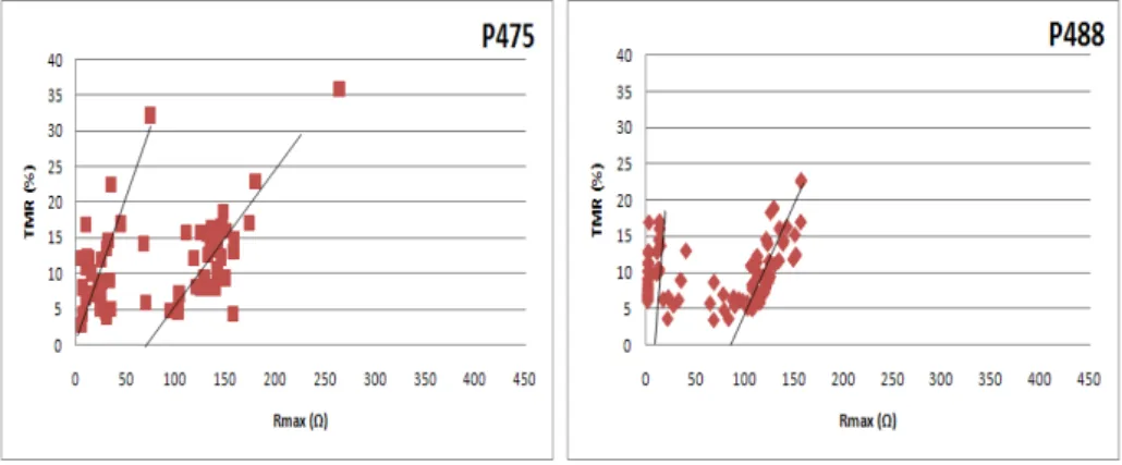
In figures 3.3, 3.4 and 3.5 are presented the cumulative distribution functions (CDF) found for the TMR of each wafer. The CDF describes the probability of finding a value less than or equal to x. Wafers P475 and P488 (natural oxidation) are the ones with smaller TMR: typically under 40%. Although wafers P480, P487 (double oxidation) and P515 (plasma oxidation) present similar ranges of TMR, the median TMR for P515 is much smaller than for the other two wafers. This may indicate the presence of more pinholes in the junctions of P515 (plasma oxidation) than in P480 and P487 (double oxidation).
Using graphical representations of the data such as the ones shown in fig-ures 3.6, 3.7 and 3.8 it is possible to determine the quality of the wafers (amount of shunt and the values of serial resistance).
Figure 3.3: Distribution of TMR in wafers processed with simple natural oxi-dation, P475 (left) and P488 (right). The different lines correspond to different junction sizes.
Figure 3.4: Distribution of TMR in wafer processed with plasma oxidation, P515. The different lines correspond to different junction sizes.
Figure 3.5: Distribution of TMR in wafers with double layer of MgO, P480 (left) and P487 (right). The different lines correspond to different junction sizes.
Figure 3.6: TMR as a function of Rmax for for wafers P475 (left) and P488
(right) - natural oxidation.
Figure 3.7: TMR as a function of Rmaxfor wafer P515 - plasma oxidation.
Figure 3.8: TMR as a function of Rmaxfor wafers P480 (left) and P487 (right)
Comparing the results obtained for the wafers P475 and P488, processed with natural oxidation, we see that they are very similar, indicating that the pressure of oxygen in the chamber during oxidation has little influence in the magnetoresistive properties of the junctions.
The results of wafers P480 and P487 (double oxidation), indicate less shunt in wafer P487. This is associated with the difference in the angles used during the IBE and indicates that the second choice, i.e. a single angle of 45°, is in fact better than the previously used processing method. The maximum values of resistance achieved in both wafers are very different, which is a consequence of the difference in associated RA values.
The most relevant parameters determined through the mapping and that will be crucial later to correct the breakdown results are summarized in table 3.2.
Nominal area (nm2) Diam. ext. (nm) R
serial(Ω) 500×500 10 100×100 70 P475 140×40 55 90 100×50 190 Natural 50×50 60 oxidation 500×500 10 100×100 70 P488 140×40 50 80 100×50 100 50×50 60 500×500 10 100×100 50 P480 140×40 60 100 100×50 125 Double 50×50 50 oxidation 500×500 10 100×100 60 P487 140×40 20 100 100×50 125 50×50 50 500×500 10 100×100 90 Plasma P515 140×40 50 110 oxidation 100×50 150 50×50 130
Table 3.2: Extension of diameter and serial resistance values for each size and each analysed wafer.
An estimation of the RA value for each wafer was carried out using a plot of TMR as a function of RA calculated, for each cell, as
RA = (Rmin− Rserial).π
(d + ext)2
4 (3.1)
where d is the nominal diameter and ext is the extension of diameter (see table 3.2). The values determined for the RA product are presented in table 3.3.
Process Wafer Expected RA (Ω.µm2) Estimation of RA (Ω.µm2) Natural P475 10 3 oxidation P488 10 1 Double P480 20 14 oxidation P487 20 15 Plasma ox. P515 30 20
Table 3.3: Expected and estimated RA values for each wafer.
Comparing the results obtained with the values expected we see that, in the case of the naturally oxidized wafers, the difference between expected and estimated attains larger values, above 70%. This is a result of the large resistance shunt due to re-deposition of the junction sidewalls, that results in an apparently lower RA.
3.3
Breakdown results
The ramp breakdown test presented in chapter 2 was performed in all samples. The first problem to solve was the definition of the breakdown point. There are two distinct types of breakdown: sharp and progressive. The first type corresponds to a voltage at which the junction presents an abrupt change of behaviour, a great decrease of resistance and TMR (fig. 3.9) and the breakdown point is clearly defined. On the other hand a junction can break progressively, presenting a gradual change of behaviour. In this case a criteria to define break-down must be chosen. A memory cell needs to have constant behaviour in order to be reliable so the breakdown point was defined as the point at which the resistance achieves a value equal or lower than 80% of the initial value (fig. 3.9). After attaining this point the junction is considered to be no longer reliable or usable.
The most typical breakdown behaviour for each type of wafer tested is rep-resented in figure 3.9 and information about the type of breakdown observed is summarized in table 3.4. For wafers P475 and P488 (natural oxidation) the vast majority of the junctions broke progressively, while P515 (plasma oxida-tion) presents the two types of breakdown. Finally for P480 and P487 (double oxidation) the most typical breakdown process is sharp. A direct conclusion is that the double oxidation process does in fact produce junctions with much lower probability of pinhole existence, since progressive breakdown is usually as-sociated with existing pinholes in the tunnel barrier that become larger with the successive application of voltage through the junction. In the graphic showing the sharp breakdown (fig. 3.9, bottom) there is an increase of TMR and min-imum resistance as further pulses are applied. This occurs when short-circuit paths on the side walls of the pillar, formed by sidewall re-deposition during the ion milling process, are disrupted by electromigration. This process is usually called burning of the re-deposition in the sidewalls.
We have seen that junctions in different wafers may break in different ways. However, what is desirable in a functional MRAM cell is that it can work for a long period of time within a certain range of parameters without breaking. For cells being written by magnetic field under the thermally assisted write scheme,
Figure 3.9: Typical breakdown of a junction from a wafer with natural oxidation of the MgO layer (top), plasma assisted oxidation (middle) and double oxidation (bottom). The inset of each plot shows the change in TMR with the application of the pulses.
Breakdown Natural ox. Plasma ox. Double ox. type P475 P488 P515 P480 P487 Progressive 95% 100% 40% 5% 8%
Sharp 5% 0% 60% 95% 92%
Table 3.4: Statistics of the breakdown behaviour observed on circular dots for each of the tested wafers.
Figure 3.10: Breakdown voltage results for junctions with a diameter of 500 nm (left) and 100 nm (right).
it is necessary to achieve a power density of 10 to 30 mW/µm2. For cells
operating under the spin transfer torque switching write scheme, the current density needs to be in the range of 106− 107 A/cm2. Therefore the different
types of barrier need to be evaluated for breakdown as a function of voltage, but also as a function of power density, Pd, and current density, Id, for each
wafer. These two parameters are calculated as Pd=
V2
R.A Id = V
R.A (3.2)
where V, R and A are the corrected values of voltage, resistance and area obtained by V = Vmeas Rmeas− Rserial Rmeas R = Rmeas− Rserial A = π (d + ext)2 4 (3.3) The subscript meas indicates the value that was measured during the test, i.e. the one with no correction.
Looking at the results for the breakdown voltage (fig. 3.10) it is clear that the wafers with double layer of MgO are more resistant and can remain functional under higher voltages. The results for the wafers with simple natural oxidation show reduced endurance to applied voltage, which is consistent with pre-existing pinholes in the tunnel barrier. For wafer P515 (plasma oxidation) the two types of breakdown are present, but no sharp breakdown was found in junctions with 500 nm of diameter, so the results are similar to those found for the natural oxidation wafers. However, in the dots of 100 nm some junctions presented sharp breakdown which is shown in figure 3.10 (right) as the presence of two populations in the red curve regarding wafer P515. More than 30% of junction breakdown occurs at the same voltages as the double natural oxidation barriers. The power density results for breakdown (fig. 3.11) indicate that, for both sizes, the plasma barrier wafer P515 starts to breakdown at lower voltages com-pared to the other oxidation methods. The double natural oxidation MgO wafers achieve the highest power density levels. However the increase over simple nat-ural oxidation barriers is small.
Figure 3.11: Results of power density at breakdown point for junctions with a diameter of 500 nm (left) and 100 nm (right).
Figure 3.12: Results of current density at breakdown point for junctions with a diameter of 500 nm (left) and 100 nm (right).
Natural ox. Plasma ox. Double ox.
P475 P488 P515 P480 P487
Vbkd (V) 0.66 0.58 1.29 2.11 1.92
Id (A/cm2) 3.66×10⁷ 2.27×10⁷ 1.02×10⁷ 2.18×10⁷ 1.34×10⁷
Pd (mW/µm2) 233.9 231.6 133.0 461.1 250.5
Table 3.5: Mean values of breakdown voltage, current density and power density for the 100 nm dots of each wafer.
Natural ox. Plasma ox. Double ox.
P475 P488 P515 P480 P487
Vbkd (V) 1.03 0.68 0.83 1.68 1.97
Id (A/cm2) 1.65×10⁷ 2.09×10⁷ 6.13×10⁶ 7.82×10⁶ 1.07×10⁷
Pd (mW/µm2) 168.8 141.6 52.6 133.6 214.3
Table 3.6: Mean values of breakdown voltage, current density and power density for the 500 nm dots of each wafer.
The current density results (fig. 3.12) indicate an apparent dependence in RA product: wafers with higher RA product have smaller values of current density at the point of breakdown. For spin torque applications it is desirable that the junction can withstand high currents, to achieve the reversal of the storage layer. Therefore, given the results obtained, the ideal would be combine the use of double layer of MgO with lower RA product. This way it should be possible to obtain junctions capable of enduring the flow of high currents without breaking. The average results for the three parameters discussed above are summarized in tables 3.5 and 3.6.
The influence in the breakdown of the direction in which the current flows through the junction, as set by the polarity of the applied voltage, was also studied. In this work we will designate positive current as the current that flows through the junction in an ascending direction and negative current flows in descending direction (fig. 3.13).
From the results in figures 3.14 and 3.15 we conclude that the direction of the current has no influence in the breakdown voltage of the wafers with simple natural oxidation and plasma oxidation. However, different breakdown behaviours were observed in the wafers with double oxidation (fig. 3.16) in 100 nm dots. Due to the limited number of this type of junctions available this is a result to be confirmed by other measurements.
Elliptical dots (100×50 and 140×40) were also measured. Regarding the parameters presented above (voltage, power density and current density) they do not seem to be an improvement to the other junctions, neither do they behave significantly worse. It seems that the most important parameter is area and not shape or perimeter. The dominant type of breakdown for each wafer also doesn’t change significantly between circular and eliptical dots. No assymetry in breakdown behaviour related with the direction of the current was found with in any of the elliptical dots tested.
Figure 3.13: Representation of two different currents flowing through a mem-ory cell in opposite directions, showing the definitions of positive and negative current.
Figure 3.14: Comparison of voltage breakdown results obatined with the current flowing in ascending and descending directions for dots of 100 nm of diameter of both wafers with naturally oxidized MgO, P475 (left) and (P488).
Breakdown Natural ox. Plasma ox. Double ox. type P475 P488 P515 P480 P487 Progressive 95% 93% 5% 8% 25%
Sharp 5% 7% 95% 92% 75%
Table 3.7: Statistics of breakdown type for the eliptical dots (100×50 and 140×40) of each wafer.
Figure 3.15: Comparison of voltage breakdown results obatined with the current flowing in ascending and descending directions for dots of 100 nm of diameter of wafer P515 (plasma oxidation).
Figure 3.16: Comparison of voltage breakdown results obatined with the current flowing in ascending and descending directions for dots of 100 nm of diameter of both wafers with double oxidation, P480 (left) and P487 (right).
3.4
Summary
The different pressure of oxygen in the deposition chamber has little effect in the behaviour of the wafers with naturally oxidized MgO layer. Wafers with double natural oxidation MgO exhibit a much smaller
occur-rence of progressive breakdown events.
Breakdown voltage results are higher for wafers with double natural oxi-dation MgO.
Apparent dependence with RA in the results of current density at the point of breakdown was detected.
Asymmetric breakdown behaviour with the direction if current through the junction was found only for wafers P480 and P487 (100 nm dots). Progressive breakdown behaviour occurs mostly in pillars of 500 nm
nom-inal diameter, explained by the large area of the pillar that increases the probability for pinholes to occur in the barrier.


![Figure 2.5: Photo (left) and schematic [16] (right) of the QSW tester.](https://thumb-eu.123doks.com/thumbv2/123dok_br/15645722.1058168/25.892.191.694.188.566/figure-photo-left-schematic-right-qsw-tester.webp)