Miguel Mota Prego Rosmaninho
Electrodeposition of Bi
2
Te
3
Nanomaterials for Thermoelectric
generators
Department of Physics and Astronomy
Faculty of Sciences of the University of Porto
Electrodeposition of Bi
2
Te
3
Nanomaterials for Thermoelectric
generators
Thesis submitted to the
Faculty of Sciences of the University of Porto
in partial fulfilment of the requirements
for the degree of
Master in Physics Engineering
Supervisor: Dr. André Miguel Trindade Pereira
co-Supervisor: Dra. Mariana de Jesus Paiva Proença
Department of Physics and Astronomy
Faculty of Sciences of the University of Porto
i
“When you reach for the stars, you may not quite get them, but you won’t come up with a handful of mud either.”
iii
Acknowledgements
First and foremost I want to thank my supervisor, André Miguel Trindade Pereira for his dedication, patience and support. I am very thankful for his continuous resourcefulness and for providing me the opportunity to develop this work. This would not be possible without him. I've learnt a great deal of things and it is all thanks to his efforts.
I also want to thank my co-supervisor, Dra. Mariana de Jesus Paiva Proença for all she taught me, for all the patience to deal with me and to expertly explain so many techniques and experimental details. Special attention and thanks to all the inanoE members for the interest shown in this work and the investment made in me.
Special thanks to my family, more specifically my parents and my brother for making me who I am today and for giving me all the love and caring that very few people have the chance to experience. You have given me what I can never repay you.
I want to also thank Ana Pires, thanks to you several of my more boring days were a lot funnier and without your help, I'd have burnt many more things in those ovens. You've been quite important for this work and, even though we still do not understand why, I want to thank you for trying to enter this area by depositing Bi2Te3 in the electron beam deposition, even if it wasn't your plan.
I would like to also show my gratitude to Bernardo Bordalo and Filipe Falcão for all the laughing, support and interest you have shown in our friendship. This would definitely be much harder experience without the relaxation periods you have given me and all the patience you have shown. Thank you, really. I would like to also thank Óscar Moutinho, Ana Rodrigues, Ana Fernandes and Eliana for the friendship we share and the support you gave me. Thanks for all the good times. I would also like to thank all the members of IFIMUP-IN, like Célia Sousa and João Ventura but I would like to give a special focus to Francisco Carpinteiro for the great work and time he dispensed to help me in this. A part of this work would have not been possible without him and it was quite an important personal achievement what he helped me optimize.
It is quite important to refer all the hard work and kindness shown to me by "UNIDADE DE MICROSCOPIA ELETRÓNICA" of Vila-Real specifically Lisete Fernandes and Pedro Tavares. I would also like to thank Sofia Teixeira, the PEEC student who diligently did the COMSOL simulations and has shown so much interest in this area.
Finally, the most important person I have in my life and which I need to thank the most, Ana Cláudia Teixeira thank you for all your dedication, love and patience for me. You have given me more support than I could have thought possible and this work is, in part, your doing and yours as well. Thank you, really.
v
Resumo
O consumo energético atual é o mais alto de sempre, aumentando por isso a procura por novos e inovadores geradores baseados em métodos verdes. É imperativo que estes dispositivos sejam sustentáveis e usem fontes não convencionais para conquistarem o seu espaço. É aqui que a tecnologia termoelétrica é única, conquistando o grande mercado que é o de energia calorífica desperdiçada. O princípio por detrás destes materiais é utilizar um gradiente de temperatura para gerar uma corrente elétrica, utilizando o efeito de Seebeck e Peltier.
Este trabalho inicia-se com uma breve explicação das técnicas utilizadas assim como das desenvolvidas unicamente para a medição de propriedades termoelétricas. Uma explicação completa do método de eletrodeposição é dada, seguida do método de produção da alumina anódica nanoporosa. O trabalho continua com a elaboração sobre os filmes finos de Bi2Te3
electrodepositados no regime potentioestático. Aqui mostrou-se a habilidade de criar ambos o tipo p e n de Bi2Te3 nomeadamente estudando a estequiometria, cristalografia, morfologia e processos de
crescimentos das amostras. Uma relação foi estabelecida entre o potential de eletrodeposição aplicado e estas propriedades, assim como o efeito nas amostras de variar a concentração dos iões de Bi e Te no eletrólito.
Utilizando o conhecimento obtido na preparação destes filmes finos, o crescimento de nanofios de Bi2Te3 assistida pela alumina anódica nanoporosa será mostrada. Uma forte relação entre o potencial
de eletrodeposição e a taxa de deposição, preenchimento dos poros, estequiometria e cristalografia dos nanofios é apresentada, tendo sido concluído que potenciais baixos mostram um crescimento cristalino quase único. Além disso, completo preenchimento dos poros com a estequiometria quase perfeita de 2:3 de Bi/Te será demonstrada, que rapidamente se torna amorfa, com menor raio dos nanofios e uma estequiometria muito distinta com o crescimento deste potencial. Os últimos resultados encontram-se baseados na aplicação dos resultados anteriores na criação de um protótipo de um microgerador. Só um dos designs desenvolvidos foi produzido, utlizando técnica litográficas para criar um conjunto de 100 pilares com 500 μm de diâmetro, criando assim um dispositivo com uma área de 1 cm2. Baseado na criação de pilares de Bi2Te3 criados via
eletrodeposição, foi possível provar que dispositivos tanto de tipo p como de tipo n foram desenvolvidos e que estes são capazes de produzir um potencial constante acima dos 10 μV. Simulações numéricas foram também realizadas com estruturas similares o que mostrou que o dispositivo desenvolvido apresenta valores abaixo do teórico. Uma metodologia foi também proposta para construir e desenvolver um dispositivo completamente funcional que contenha pilares de ambos os tipos, p e n, que irá mostrar uma potência muito superior e que será um microgerador completamente aplicável.
vii
Abstract
Present energy consumption is the highest that has ever been, boosting the need for new, innovative generators based on green methods. It is imperative that these devices are self-sustained and use non-conventional sources to conquer their space. This is where the thermoelectric technology can be unique, by conquering the big market that is wasted heat energy. The physical principle behind these materials is utilizing a gradient of temperature to generate an electrical current, the so called Seebeck and Peltier effect.
This work starts with a brief overview of the techniques used as well as the ones developed solely for the measurement of thermoelectric properties. A thorough explanation of the electrodeposition process is given, followed by the production of porous anodic alumina templates. The work proceeds with the elaboration of thin films structures of Bi2Te3 electrodeposited in a potenstiotatic regime. Here
was shown the ability to create both p and n type Bi2Te3 namely by studying the stoichiometry,
crystallography, morphology and general growth processes of the samples. A relation was established between the electrodeposition potential applied and these properties, as well as the effects of varying the concentration of Bi and Te ions in the electrolyte on the samples.
By using the knowledge obtained in the thin films preparations, the growth of Bi2Te3 nanowires
assisted by the porous anodic alumina template will be shown. A strong relation between the electrodeposition potential and the deposition rate, pore filling, stoichiometry and crystallography of the nanowires is presented, having been concluded that low deposition potentials show almost single crystalline growth. Furthermore, complete pore filling with a 2:3 Bi/Te ratio will be shown, which quickly turns amorphous, with smaller nanowire radius and very distinct stoichiometry with the growth of this potential.
The final results are based on the application of all the previous work (chapter 3 and 4) in the creation of working microgenerator prototypes. Only one of the designs was produced using lithographic techniques to create an array of 100 pillars with 500 μm in diameter making a device with an area of 1 cm2. Based on the creation of Bi2Te3 pillars made via electrodeposition, it was possible to prove that
both n and p type devices were produced and that these are capable of producing a continuous potential of over 10 μV. Numerical simulations were also performed with similar structures which showed that our developed device presents much lower values. It has also been proposed one methodology to build and develop a fully functional device encompassed of both p and n type pillars which should prove to have much higher power output and to be an applicable microgenerator.
ix
Contents
Chapter 1 Introduction
1
1.1 Thermoelectric effect
1
1.2
Thermoelectric efficiency
3
1.3
Thermoelectric Bulk materials
5
1.3.1
Skutterudites and Clathrate
5
1.3.2
Oxides
5
1.3.3
Composites: Nanoinclusions
5
1.4
Bismuth Telluride (Bi
2Te
3)
6
1.5
Nanostructuring
7
1.5.1
Supperlattices and quantum wells
8
1.5.2
Nanowires and nanotubes
8
1.6
Motivation and objectives
9
Chapter 2 Materials preparation and experimental set-ups
11
2.1
Introduction
11
2.2
Fabrication of nanomaterials
11
2.2.1
Electrodeposition process
11
2.2.2
Thin film preparation
12
2.2.3
Porous anodic alumina templates
14
2.2.4
Electrodeposition of nanowires
15
2.3
Characterization techniques
16
2.3.1
Profilometer
16
2.3.2
SEM/EDS analysis
16
2.3.3
X-ray diffraction analysis
17
2.4
Conductive layer deposition methods
18
2.4.1
Sputtering
18
2.4.2
Thermal evaporation
18
2.4.3
Electron beam deposition
19
2.5
Direct laser writing
19
2.6
Thermoelectric properties
19
2.6.1
Seebeck coefficient measurement
19
x
2.7
Electrical resistivity
21
2.8
Benchmark set-up for thermoelectric devices
21
Chapter 3 Electrodeposition of Bi
2Te
3thin films
23
3.1
Introduction
23
3.2
Results and discussion
23
3.2.1
Electrodeposition analysis
23
3.2.2
N type electrolytes results
27
3.2.3
P type electrolytes results
31
3.2.4
Seebeck coefficient and electrical conductivity measurements
36
3.3
Conclusion
38
Chapter 4 Electrodeposition of Bi
2Te
3nanowire arrays
39
4.1
Introduction
39
4.2
Results and discussion
39
4.2.1
Electrodeposition current transients
39
4.2.2
Morphological characterization
40
4.2.3
Stoichiometry analysis
43
4.2.4
Crystallographic structure
43
4.3
Conclusions
45
Chapter 5 Fabrication of Bi
2Te
3microgenerators prototypes
47
5.1
Introduction
47
5.2
Working prototype
47
5.3
Design of functional thermoelectric microdevice concept
49
5.4
Conclusion
53
Chapter 6 Conclusions and future work
55
6.1
Conclusions
55
6.2
Future work
56
List of Publications and Communications
57
Publications
57
Oral Communications
57
Poster communications
57
Other scientific work
57
xi
List of Figures
Figure 1.1
(a) World energy consumption reported in the bp statistical review of World Energy
(b) Thermoelectric devices growth projections reported in ObservatoryNano june 2011. ... 1
Figure 1.2
Several examples for the use of thermoelectrics in today's market, adapted from [3]. 2
Figure 1.3
Best thermoelectric for each temperature range ... 3
Figure 1.4
Most recent and successful developments in thermoelectric materials [13]. ... 4
Figure 1.5
(a) Thermoelectric device efficiency with T
c=300K [14]. (b) Generation efficiencies of
the most common energy sources. ... 4
Figure 1.6
Crystal structures of (a) the skutterudite CoSb
3and (b) a type-I clathrate [17]. ... 5
Figure 1.7
(a) Nano-inclusion of Ag-Sb in a AgPb
18SbTe
20matrix [21]. (b) zT of 0.6% ErAs
nanoparticles inside an In
0.53Ga
0.27Al
0.20As matrix [20]. ... 6
Figure 1.8
Crystal structure of Bi
2Te
3[22]. ... 7
Figure 1.9
Plot of zT as a function of nanowire width along the x, y and z directions on Bi
2Te
3[22].
... 7
Figure 1.10
(a) Bulk zT value vs doping and (b) zT vs nanowire thickness [23]. ... 7
Figure 1.11
(a) Plot of zT vs layer thickness for the (1) a-b plane, (2) a-c plane of Bi
2Te
3and the
dashed line represents the bulk's zT [24]. (b) Example of a superlattice [25]. ... 8
Figure 1.12
Scanning electron microscopy images of (a) highly ordered nanopores in PAA, [(b) and
(c)] Bi
2Te
3nanowire array in a PAA template: (b) top [29] and (c) cross-sectional [27] views. The
numbers in (c) correspond to: 1) bottom gold layer, 2) nanowires, 3) nanowires with outstanding
length, and 4) hemispherical overgrowth on top of the membrane. ... 9
Figure 2.1
Three electrode cell method schematic [36]. ... 12
Figure 2.2
Three electrode set-up used for the electrodeposition of thin film structures, adapted
from [36].
... 13
... 13
Figure 2.3
SEM top image of the result on the PAA organization after (a) only the first and (b) the
second anodization [36]. ... 15
Figure 2.4
Three electrode set-up used for the electrodeposition of nanowires, adapted from
[36].
... 15
Figure 2.5
Typical EDS result of Bi
2Te
3samples, in this particular case, on a Pt substrate. ... 17
Figure 2.6
Schematic representation of the Seebeck coefficient measurement apparatus created
for this project. ... 20
Figure 2.7
Seebeck coefficient measurement of (a) a pure iron sample and (b) a copper stripe for
calibration.
... 21
xii
Figure 2.8
Four terminal sensing diagram. The wires 1 and 4 are used for current injection while
the wires 2 and 3 are used for potential readings. ... 21
Figure 2.9
Benchmark set-up for thermoelectric devices. ... 22
Figure 3.1.
Current transients measured during the deposition process of the thin films on a Pt
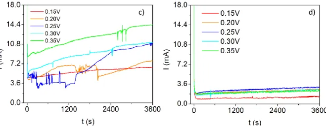
covered Si substrate using different electrolytes: (a) n-type, (b) 40%EG n-type, (c) p-type and (d)
40%EG p-type. ... 25
Figure 3.2.
Deposition curves of the samples electrodeposited at 0.25V, for different times (15m,
20m, 45m, 1h and 1h15m), on Cu stripes using the n-type electrolyte. ... 25
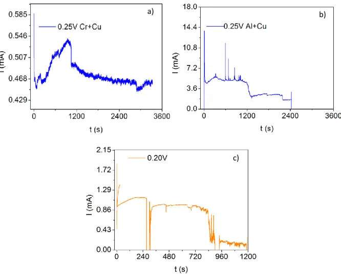
Figure 3.3.
Deposition curves at fixed potential on different substrates such as (a) glass with a Cr
seed layer covered with 75 nm copper thin film, (b) Al seed layer with 75 nm copper and (c) ITO
substrate.
... 26
Figure 3.4.
Profilometer results on a (a) 0.20 V sample made in the 0% EG n type and (b) 0.20 V
sample made in the 40% EG n type electrolyte electrolyte. ... 27
Figure 3.5.
Thickness measurement results for several electrodeposition potentials with the same
duration of (a) 0% EG n type electrolyte and (b) 40% EG n type electrolyte. ... 27
Figure 3.6.
SEM results of the 0%EG n type electrolyte deposited for 5 minutes at the potential of
(a) 0.10 V, (b) 0.15 V and (c) 0.20 V. ... 28
Figure 3.7.
SEM results of the 40%EG electrolyte deposited for 1h at the potential of (a) 0.15 V,
(b) 0.20 V, (c) 0.25 V, (d) 0.30 V and (e) 0.35 V. ... 29
Figure 3.8.
Comparison of the effect of the electrodeposition potential in the stoichiometry of
the samples using 0%EG and 40% EG n type electrolytes. ... 30
Figure 3.9.
XRD results of the samples of (a) 0% EG n type and (b) 40% EG n type electrolyte. .... 31
Figure 3.10. Cell parameter variations with applied potential (a) for the a direction, (b) c direction
and (c) total Volume. ... 31
Figure 3.11. Profilometer results on a (a) 0.20 V sample made in the 0% EG p type and (b) 0.20 V
sample made in the 40% EG p type electrolyte. ... 32
Figure 3.12. Thickness measurement results for several electrodeposition potentials with the same
duration of (a) 0% EG p type electrolyte and (b) 40% EG p type electrolyte. ... 32
Figure 3.13. SEM images of the 0%EG p-type electrolyte samples electrodeposited at (a) 0.15 V, (b)
0.20 V and (c) 0.25 V. ... 33
Figure 3.14. SEM results of the 40%EG electrolyte deposited for 1h at the potential of (a) 0.15 V,
(b) 0.20 V, (c) 0.25 V, (d) 0.30 V and (e) 0.35 V. ... 33
Figure 3.15. SEM images of growth abnormalities in the (a) 0.15 V 0%EG and (b) 0.20 V 40%EG
samples.
... 34
Figure 3.16. Effect of the electrodeposition potential on the sample's stoichiometry using the 0%
EG and 40% EG p-type solutions. ... 35
Figure 3.17. XRD results of the (a) 0% EG p type and (b) 40% EG p type electrolyte samples. ... 36
Figure 3.18. Seebeck coefficient measurement of a 0% EG sample on Cu stripe deposited at 0.25V.
xiii
Figure 4.1.
Representation of the electrodeposition current transients monitored during (a) a
typical NWs deposition process at 0.3 V, and (b) the NWs deposition at different applied potentials. ..
... 40
Figure 4.2.
Cross section SEM views of the whole PAA with Bi
2Te
3nanowires deposited at (a) 0.30
V, (b) 0.50 V and (c) 0.75 V for 8 h. ... 41
Figure 4.3.
Bottom and cross section SEM views of the NWs electrodeposited at (a) 0.15 V, (b)
0.20 V and (c) 0.25 V for 30 min. ... 41
Figure 4.4.
Cross section SEM views of the NWs electrodeposited at (a) 0.15 V, (b) 0.20 V and (c)
0.25 V for 30 min. ... 42
Figure 4.5.
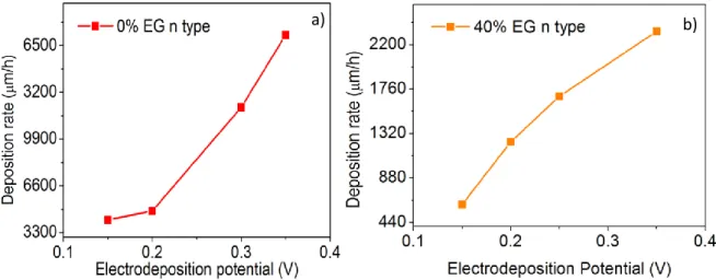
Rate of deposition based on the estimation of the NWs length from SEM
cross-sectional images. ... 42
Figure 4.6.
Effect of the electrodeposition potential on the nanowire's stoichiometry. Inset shows
a typical EDS measurement of the nanowires in the PAA. ... 43
Figure 4.7.
(a) XRD spectra of the nanowires electrodeposited in the PAA templates at different
potentials. (b) Variation of the volume of the unit cell with the applied potential. ... 44
Figure 5.1.
Photographic proof of the (a) flexibility and (b) small size of the devices developed. . 48
Figure 5.2.
Device potential measurements of (a) p type pillars and (b) n type pillars on flexible
substrate.
... 48
Figure 5.3.
COMSOL simulation of a six pillar system of Bi
2Te
3showing the (a) electrical potential
and (b) current density with a ΔT of 3 ºC. ... 49
Figure 5.4.
SU-8 film thickness in function of rotation speed [57]. ... 50
Figure 5.5.
Fully functional thermoelectric microgenerator build diagram ... 52
xv
List of Tables
Table 1. Electrodeposition potential effect on several thin films properties... 37
Table 2. Nanowire length and crystallite size measured at room temperature for the different applied
potentials... 44
xvi
xvii
Nomenclature
Bi
2Te
3Bismuth telluride
EDS
Energy-dispersive X-ray spectroscopy
ITO
Indium tin oxide
PAA
Porous anodic alumina
PMMA
Poly(methyl methacrylate)
SEM
Scanning electron microscope
XRD
X-ray diffraction
Introduction
1
Chapter 1
Introduction
1.1 Thermoelectric effect
The permanent requirement for energy in the world and the rise on environmental awareness boost the demand for new clean sources. The most prominent energy sources are based on combustion or heating processes [Figure 1.1 (a)], with 60% of their energy wasted in the form of heat [1]. This opens the pathway for heat recovering by converting it into electrical energy for power supply devices. Thermoelectric technology arises as the best solution for this issue since it has the ability to create current from a temperature gradient (and vice-versa). Furthermore, it has no moveable parts, it is emission free, silent and a vibration free principle. It also presents very low maintenance costs, the ability to control the amount of wasted heat leaked into the environment and a very user friendly working process, which are vital advantages for the market. In fact, this technology already represents a market of 175-200 million Euros, as reported in ObservatoryNano june 2011 [1] [Figure 1.1 (b)] and, even though it is a market of millions, thermoelectric devices are seen as being in the prototype phase.
Figure 1.1 (a) World energy consumption reported in the bp statistical review of World Energy [2]. (b) Thermoelectric devices growth projections reported in ObservatoryNano june 2011 [1].
Several predictions state that it will easily grow 10-100 times due to the optimization and new low cost manufacturing processes being reported in the most recent scientific works [3-6]. One of the most important characteristics is that it works in parallel to other energy sources instead of competing with them. As an example, on the transportation sector alone, these devices could quickly, and very conservatively, represent a 7 billion euro market [1], without even counting the market for thermal control that thermoelectric air conditioners or seat heater/cooler systems could bring. Several companies have already started investing and proving the power behind this concept, such as Vodafone's Power Pocket, BMW's award winning thermoelectric generator [7] or Fujifilm's high performance organic thermoelectric [8] [Figure 1.2]. All of these applications are but a fraction of its potential uses, since it has predicted uses in medicine, where our body heat versus air temperature
Introduction
2
could be used to fuel small devices such as pacemakers, in biomass facilities, where the heat released during fermentation could be harvested and many others situations [4].
Figure 1.2 Several examples for the use of thermoelectrics in today's market, adapted from [4].
There are already a few configurations for thermoelectric devices, but the most common are based on the working principle represented in Figure 1.2. The basic unit of a thermoelectric cell is composed of an n-type and a p-type semiconductor (two legs), connected to each other via a conducting material. The use of a combination of p and n-type is due to the opposite signal of the respective Seebeck coefficient which is a condition to ensure the current flow through both legs. The main thermoelectric materials used are thus semiconductors and insulators [Figure 1.3 (a)], due to the high Seebeck coefficient they present, when compared to the very low values of metals and other conductive materials. In fact, the Seebeck phenomenon was discovered in 1821 by Thomas Seebeck and gave the relation between the electrical potential and temperature gradient [9]:
(1.1)
where S is the Seebeck coefficient, which is negative for n-type semiconductors and positive for p-type semiconductors. Microscopically, when an n-p-type or p-p-type material is under a temperature gradient ( ) between the two extremities, the carriers on the hot side (Th) of the bar will have a
Introduction
3
of these carriers to diffuse to the other side is much larger than the opposite happening, creating a concentration of charge on the cold side (Tc) which leads to an electrical field (E) [Figure 1.3 (c)] [11].
This creates a current from the hot extremity to the cold extremity in the case of holes and the inverse in the case of electrons. The Peltier effect uses the inverse principle, where an electrical field will dislocate these carriers from one side to the other. These high energy carriers will then heat up one side of the bar while the other side cools down, creating a temperature gradient.
Figure 1.3 Best thermoelectric for each temperature range [10]. Schematic representation of the thermoelectric effect showing carriers (b) mean free path length and (c) concentration along the bar [11].
These points are the main reason to use p and n type [Figure 1.2] to ensure that the current passes through.
1.2 Thermoelectric efficiency
It is well known that for a thermoelectric generator, the maximum efficiency of a device will be [12]:
(1.2)
where Th and Tc are the hot and cold side temperatures, respectively, and zT is the figure of merit.
The zT depends of the thermal transport properties of the material and is expressed as [13]:
(1.3)
where is the electrical conductivity, K is the thermal conductivity and T is the temperature.
This figure of merit was a major limitation for thermoelectrics since, as seen in Figure 1.4, until the early 2000's its maximum value was limited to 1. As is visible in Figure 1.5 (a) these low zT values do not allow high efficient thermoelectric devices to be developed.
Nowadays this limitation has been broken due to the implementation of several nanomaterials which had a tremendous increase of zT, to values of over 2.4 [5].
Introduction
4
Figure 1.4 Most recent and successful developments in thermoelectric materials [14].
That improvement came mainly by increasing the phonon scattering within the unit cell through the creation of rattling structures or point defects such as interstitials, vacancies or by alloying. This has enhanced interfacial scattering using multiphase (disordered) nanocomposites or nanoscopic confined structures with a strong impact namely decreasing the thermal conductivity, raising the zT value and will be discussed in detail in the next section.
The impact of increasing the zT value is crucial for current scientific research, as indicated in Figure 1.5 (a), where in ideal conditions the thermoelectric generator efficiency could reach values as high as 45%. This, combined with their ability to be used in parallel to traditional power sources [Figure 1.5(b)] with efficiencies almost as high as them, could highly improve energy yields.
Figure 1.5 (a) Thermoelectric device efficiency with Tc= 300 K [15]. (b) Generation efficiencies of the most common energy
sources [16].
Introduction
5
1.3 Thermoelectric Bulk materials
The main strategies to increase the phonon scattering within the unit cell are being done in bulk materials, namely in skutterudites, clathrates, oxides and nanoinclusions.
1.3.1 Skutterudites and Clathrate
Skutterudites and clathrates possess interstitial voids in their unit cell, which can be filled with doping elements, in a cage-like structure [Figure 1.6 (a) and (b)]. The introduction of doping elements in the unit cell will lead to big atomic displacement which will translate in a rattling movement of the dopant in their site [17]. This vibration's frequency will vary with the atom, thus allowing one to tune the phonon scattering or to develop a multi-doped skutterudite which will scatter a wide range of phonons. Skutterudites are used mainly for high temperature ranges, having reached values of 1.7 zT at 850 K [18]. Still they have strong liabilities such as: long production times and the use of toxic elements like arsenium. The production times have been decreasing rapidly but the use of toxic elements is still an issue. On the other hand, clathrates use metal elements as doping agents but also use toxic elements. They are a recent technology, with many venues for potential improvements that might bring about further utilities. Still, zT's of 1.2 at 500 K have already been attained [19].
Figure 1.6 Crystal structures of (a) the skutterudite CoSb3 and (b) a type-I clathrate [19]. The zT evolution for oxides over
the last years (c) [20].
1.3.2 Oxides
Oxides are very important for high temperature, 1000 K or higher, thermoelectric materials. This kind of structure presents a zT of 1, and they are made of very common, low cost elements with no toxicity. Further development of these materials will allow the thermoelectric devices to recover heat on systems that have a high need for thermal-to-energy conversion, therefore they are the focus for big thermal power plants and big industrial high temperature devices. The interest in these materials was greatly spurred by Terasaki et al. [20] when they showed the great promise of NaCo2O4. Since
then, several new works have been appearing having further roused the interest in thermoelectrics.
1.3.3 Composites: Nanoinclusions
Inclusions are small precipitations where the composition changes slightly when compared with the matrix around it, as can be seen in Figure 1.7 (a). These can be obtained by simple industrial
Introduction
6
processes such as annealing and ball milling. They are seen as small scattering centres that dramatically increase the zT of known structures and materials. These inclusions take advantage of one of the main reasons for the increase in zT with the appearance of nano-engineering, which is the dramatic increase in the number of scattering centres for phonons without affecting the number of scattering centres for electrons. This is mainly due to the different length in the free mean path of these two types of particles. These very low cost improvements have already raised the maximum zT value of Bi2Te3 compounds by 50% to 1.56 zT [21].
Figure 1.7 (a) Nano-inclusion of Ag-Sb in a AgPb18SbTe20 matrix [23]. (b) zT of 0.6% ErAs nanoparticles inside an
In0.53Ga0.27Al0.20As matrix [22].
Another kind of nanoinclusions is the embedding of semi metallic nanoparticles into semiconductor matrices. This process is also very inexpensive, similar to the industrial processes referred above, as can be seen in Figure 1.7 (b), also having the advantage of being highly stable at high temperatures. This methodology of nanoinclusions is still in an early stage being foreseen as a good methodology to improve the zT.
1.4 Bismuth Telluride (Bi
2Te
3)
Bi2Te3 is the material with the highest zT value near room temperature, which makes it the most
commonly used material in the thermoelectric market [Figure 1.3]. Since their discovery as excellent materials for thermoelectric technology, Bi2Te3 based materials reached improvements in zT higher
than 50%, to over 1.5 zT [24]. This high efficiency is because Bi2Te3 is highly directional, which can be
explained by its typical crystal structure, as depicted in Figure 1.8. In the c direction the bounds are of Van der Waals nature while covalent and ionic on the basal plane, which translates into a three times higher electrical conductivity for this plane. Furthermore, it possesses a high Seebeck coefficient since it is a semiconductor (around -200 μVK-1
), and a low thermal conductivity (around 1.20 WK-1m
-1
). In addition, the fact that it is compatible with almost every production method brings another great advantage to this material. Typical Bi2Te3 is used as an n-type semiconductor, but it can also be used
as a p-type just by slightly changing the Bi:Te ratio. Experimentally it was observed that when there is a slight lack of Te in the composition (lower than 58%), it already presents a p-type behaviour.
Introduction
7
Figure 1.8 Crystal structure of Bi2Te3 [25].
1.5 Nanostructuring
As can be seen in Figure 1.9 and Figure 1.10, very low dimensional thermoelectrics could prove to have incredibly high zT values. This is a new line of thermoelectric research which grew in the mid 1990's and still continues on, aiming to reach record high zT values in the near future. These results were mainly obtained in two-dimensional or one-dimensional systems, which were composed of three main structures: (i) superlattices and quantum wells, (ii) nanowires and (iii) nanotubes.
Figure 1.9 Plot of zT as a function of nanowire width along the x, y and z directions on Bi2Te3 [26].
Figure 1.10 (a) Bulk zT value vs doping and (b) zT vs nanowire thickness [27].
)
)
)
Introduction
8
1.5.1 Supperlattices and quantum wells
A superlattice is a series of alternated dominions, ranging from small composition changes to possible distinct compositions, having thicknesses from a few angstrom (Å) to several nanometers [Figure 1.11]. This approach produces better zT results than their bulk counterparts due to two main reasons: (i) the density of states near the Fermi level gets enhanced by the quantum confinement; and (ii) the phonons, in a wide range of frequencies, are strongly scattered on the interfaces between the different materials. Superlattices and quantum wells were the first indicators that interfaces were the fastest and easiest way to reach high zT, which spurred the growth of the bulk counterparts. Several works based on this phenomenon have already produced zT's over 2 [5].
Figure 1.11 (a) Plot of zT vs layer thickness for the (1) a-b plane, (2) a-c plane of Bi2Te3 and the dashed line represents the
bulk's zT [28]. (b) Example of a superlattice [29].
1.5.2 Nanowires and nanotubes
Having the highest predicted zT values, as seen in Figure 1.9, these are incredibly important structures for thermoelectrics. Nanowires are already being used in medicine, to dispense more localized treatments and with lesser doses; engineering, to improve solar panels; and environmental applications, such as water purification. In thermoelectric studies, it has already enabled the appearance of thermoelectrics based on silicon with a zT of 1 at low temperatures of 200 K [30], where the bulk counterpart has yet to exceed 0.01 at any temperature. The use of porous anodic alumina (PAA) [Figure 1.12 (a)] or carbon nanotubes as templates for these wires is a recent development for thermoelectrics, still under heavy scrutiny but showing very promising results for low cost, high zT production processes. The possibility of creating large arrays of PAA filled with, for example Bi2Te3, would provide much higher zT than the bulk counterpart due to the higher number of
interfaces. Another possible approach is that of malleable thermoelectrics using these arrays of nanowires in PAA, which would improve even further the number of possible markets this technology can reach [31-33]. The possibilities of these structures for thermoelectrics are truthfully immense and many other materials, which were presented as bad thermoelectrics, have already been predicted to show zT's 1000 times bigger than their bulk counterpart when reduced to the nanoscale [Figure 1.10] [28, 29]. In order to reach the maximum zT possible, PAA has been heavily applied in the fabrication processes of thermoelectric materials, since it presents the perfect thermal transport properties for a template [Figure 1.12]. The most recent developments in this technology have been around Bi2Te3
Introduction
9
nanowires [34-39] [Figure 1.12 (b) and (c)], with reports that the zT's of these wires are already as high as the bulk's but with much lower costs. It is also important to notice that these values are for wires far too wide to bring about the predicted zT increase as in the wires presented in Figure 1.9. This means that further developments will allow the fabrication of thinner wires, which could increase the zT values to a new record.
Figure 1.12 Scanning electron microscopy images of (a) highly ordered nanopores in PAA, [(b) and (c)] Bi2Te3 nanowire array
in a PAA template: (b) top [39] and (c) cross-sectional [34] views. The numbers in (c) correspond to: 1) bottom gold layer, 2) nanowires, 3) nanowires with outstanding length, and 4) hemispherical overgrowth on top of the membrane.
1.6 Motivation and objectives
Boosted by the search of more efficient thermoelectric devices, easy, cheap and scalable production of nanostructured materials has been the main aim of the most recent developments in this technology. In accordance with this line, this work has the following objectives:
I. Production of both p and n type thin films of Bi2Te3 using the electrodeposition process.
II. Development of Bi2Te3 nanowires using a PAA template.
III. Production of a microgenerator based on the results of the thin films and nanowires.
This thesis is devoted to the development of nanostructures (2D and 1D) of thermoelectric materials based on Bi2Te3 compounds using electrodeposition technique. On the thin films, the study of best
electrodeposition parameters, namely influence of potential and time are addressed paying attention on the effect on morphological, chemical (semiconductor type) and atomic structure. Moreover, a system for the measurement of the Seebeck coefficient of thin films are also an objective of the present work.
On 1D structures, based on the results obtained on the thin films, by using alumina porous template, nanowires of Bi2Te3 will be developed. Finally, by using lithography process, the development/design
of a thermoelectric prototype will be also discussed in this thesis.
Finally, it is expected that with the results obtained in the present thesis will open new avenues on the development of cost-effective and environmentally friendly rigid and flexible thermoelectric micro/nanodevices for power generation.
Introduction
10
Materials preparation and experimental setups
11
Chapter 2
Materials preparation and experimental set-ups
2.1 Introduction
In this chapter a resumed view over the electrodeposition process of Bi2Te3 thin films, fabrication of
porous anodic alumina (PAA) membranes and nanowires growth assisted by these nanoporous templates will be described. Additionally, a brief description of the techniques used for the morphological, chemical and structural characterization of the fabricated nanomaterials will be presented, namely ray diffraction (XRD), scanning electron microscopy (SEM), energy-dispersive X-ray spectroscopy (EDS) and profilometry. On transport properties, the electrical resistivity of the thin film using the 4 contact method will be described. The detailed development of the Seebeck coefficient measurement apparatus implemented during this thesis will be presented. In order to develop the first prototypes of microdevices, clean room facilities were also used, namely the optimization of the litography process for direct writing, the use of this same direct writing and electron beam deposition. Finally, a benchmark set-up for the testing of the performance of the microgenerators fabricated under the present thesis will be shown.
2.2 Fabrication of nanomaterials
2.2.1 Electrodeposition process
Three different electrodeposition types have been commonly used for the electrodeposition of Bi2Te3:
potentiostatic deposition, potential-pulsed deposition and constant potential and constant current in pulses method [40,43].
Potentiostatic three electrode cell procedure was picked as the main deposition process due to its very high growth rates, easy reproducibility in the industrial level, very simple apparatus and experimental procedure. This technique [Figure 2.1] is connected to the need to create a stable, fully reproducible process able to properly study the behaviour of the material deposited at the working electrode while monitoring the current and potential during the growth process. At the start of this process it is necessary to perturb the system by breaking equilibrium, which is done by applying a potential in the working electrode, where the sample is connected. Since the potential of the cell needs to be measured between the working electrode and another electrode (eq. (2.1)), a well known, constant potential is paramount for the other electrode, to diminish variations and errors in the system [44]. This other electrode is entitled the reference electrode and, in our case, is Ag/AgCl (in 4M KCl) to serve as a constant reference (0.197 V vs standard hydrogen electrode; SHE).
Materials preparation and experimental setups
12
Furthermore, the use of one single electrode for the measurement of both the current and potential in the cell would mean a greater amount of error, since large currents passing through an electrode might change its potential. This is solved by using a third electrode, a counter electrode which is then used to measure the deposition current separately from the potential to ensure the most stable and repeatable process possible [44]. This electrode needs to be composed of an inert material in order to keep the solution pure of any parasitic effects. In our case this is done by a Pt mesh which closes the circuit for the current measurement. Due to the necessity of a conductive material in the working electrode for the initial creation of this current, the working electrode must always be composed of a conductive or semiconductive layer.
Figure 2.1 Three electrode cell method schematic [45].
Since the used reference electrode is Ag/AgCl, all the potentials presented in this work are in reference to it and are all presented in modulus. This point is vital to understand the effects of the electrodeposition potential and to address the relations between it and several physical properties of the samples.
2.2.2 Thin film preparation
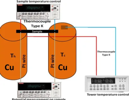
For the electrodeposition of thin films, the three electrode set-up visible in Figure 2.2, was used. The apparatus was based on the suspension of the working electrode into the electrolyte due to the need to maximize all samples length and to simplify even further the deposition process. The thin films were deposited in a common 100 ml beaker filled with 80 ml of electrolyte. The reference electrode was closely packed to the sample and finally a Pt mesh was placed on the opposite side of the reference electrode. The temperature of the room was kept constant (23 ºC) throughout the entire process. The applied potential and measured current were monitored using a remote controlled sourcemeter.
Materials preparation and experimental setups
13
Figure 2.2 Three electrode set-up used for the electrodeposition of thin film structures, adapted from [45].
In search for the best parameters possible for the stable growth of free standing Bi2Te3 thin films,
several different substrates, electrodeposition potentials and deposition lengths have been tested. A preliminary study on Cu stripes as working electrodes was conducted. These stripes were traditionally of 1.5 x 1.5 cm2, flexible and with 99.9% purity. Prior to the deposition process, these were cleaned in acetone, ethanol and deionised water for 5-10 minutes, in an ultrasounds bath. At a second stage, silicon wafers (cleaned by the same method) were also used as substrates, with a sputtered Au layer of about 50-100 nm on top to serve as the working electrode. Due to some limitations found during the deposition process on these substrates, several other materials and electrical contacts were also tested. With different success rates, ITO (Indium tin oxide), silicon, glass and PMMA (Poly(methyl methacrylate)) substrates were used. Of these, ITO, silicon and glass had a Cu layer of 50-75 nm thick evaporated on top to serve as an electrical contact. Other metallic contacts were also tested, such as Al, Al/Cu, Ti, Ti/Cu, Cr, Cr/Cu, Fe, Au and Pt. These tests allowed us to better understand the materials’ ability to withstand the solution acidity and HNO3 concentration, which traditionally attacks
conductors such as Cu and Fe [46].
Four different electrolytes have been tested all to tackle different needs of these structures, such as the creation of p-type and n-type pillars, more stable growth, solution aggressiveness and many other properties. The first one was composed of 10 mM Bi3+ and 15 mM HTeO2+ ions in 1 M HNO3 diluted in
deionised water [42]. This was done by dissolving measurable amounts of bismuth(III)-nitrate pentahydrate Bi(NO3)3・5H2O (Sigma–Aldrich) and pure Te powder (99.999%) in concentrated nitric
acid. The chemical reaction, for the formation of the thin film from this acidic solution is:
(2.2)
Bismuth telluride is insoluble in dilute nitric acid, which means that the higher rate of reduction of Te 2-combined with the lower reduction rate of Bi3+ will precipitate Bi2Te3 on the electrode surface [42].
The second electrolyte was very similar to the first one, with a higher concentration of Bi3+ by doubling the amount of bismuth(III)-nitrate pentahydrate Bi(NO3)3・5H2O (Sigma–Aldrich) in the solution and
Materials preparation and experimental setups
14
maintaining the amount of all the other reagents, having been nominated as the p-type electrolyte. The third electrolyte had the exact same concentrations of reagents in deionised water as the first one but with the addition of 40%, in volume, of ethylene glycol (EG). This is entitled as the 40%EG n-type electrolyte. The last one had the same concentrations as of the second type but with 40% total volume of EG and was designated as the 40%EG p-type electrolyte. The use of these last two electrolyes was based on recent reports, by Li et al. [47] where this compound actively assisted in the improvement of the deposition of these materials, by raising their adhesion to the conducting layer, improving film homogeneity and possibly enhancing the thickness limit. Series of five to seven samples were used, with electrodeposition potentials between 0.15 V and 0.75 V. Typical depositions lasted for 15 min up to 2 h. All depositions were conducted at room temperature in unstirred solutions.
2.2.3 Porous anodic alumina templates
The fabrication of PAA [48-52] requires high purity aluminium foils (99.999% purity), cut in squares of 1.5 x 1.5 cm2 in the case of this work. These are cleaned in acetone, pressed and then immersed in ethanol in an ultrasonic bath for 10 min. This is then followed by an electropolishing process which is used to smoothen the surface of the Al foils and remove any impurities or oxidation. This process is important to obtain a highly homogeneous membrane. The electropolishing solution is composed of 25% percloric acid (HClO4) and 75% ethanol and the process lasted for 2 min at 20 V at a
temperature below 8ºC.
This is followed by a first anodization which varied between 6-24 h in a solution with 0.3 M oxalic acid (H₂C₂O₄) at 40 V and a temperature around 4◦C. During this step, a nanoporous alumina layer is formed on top of the Al foil, creating an organized array of pits at the Al surface, which will serve as nucleation points for the nanopores growth during a second anodization process, thus forming a fully organized and structured porous membrane. The need for a second anodization [53] arises due to a poor organization of nanopores after only one of these steps, as is seen in Figure 2.3 (a). It is observed that in one step the template is highly undesired due to defects, disorder in the anodization process or the need to have a stable pores distribution throughout the entire membrane. This is visible in Figure 2.3 (b) that most of these defects are corrected after doing the second anodization. In order to do the second anodization, one first needs to remove the alumina layer of the first anodization, which was done in an aqueous solution of 0.2 M H2CrO4 and 0.4 M H3PO4 at 60◦C for
around 5-20 h [52]. Second anodizations were then performed for 40 h with the same solution and temperature as in the first anodization, in order to create a PAA with a pore diameter of around 35 nm, an interpore distance of 105 nm and a thickness of about 100 μm. After this process, the alumina template is complete and further processes are done depending on the required conditions for future applications.
Materials preparation and experimental setups
15
Figure 2.3 SEM top image of the result on the PAA organization after (a) only the first and (b) the second anodization [45].
2.2.4 Electrodeposition of nanowires
After the creation of the alumina template it is then necessary to clear the bottom pores. This is done in order to deposit a conductor for the potentiostatic deposition. This means that the bottom part of the PAA needs to be cleared of aluminium first and then cleared of the oxide layer which is blocking these bottom pores. The chemical etching of the Al foil is done in an aqueous solution of 0.2 M CuCl2 and
4.1 M HCl at room temperature for about 10 min. The alumina barrier present is then removed by chemical etching in a 0.5 M H3PO4 solution at 40◦C for 30 minutes [52]. This process enlarges the
final pore diameter to around 50-60 nm. Finally, a 50 to 100 nm Au layer was sputtered at the bottom of the opened pores to serve as the working electrode in the potentiostatic deposition.
The deposition set-up, seen in Figure 2.4, is quite similar to the thin film process but, due to the fragility of the PAA and to obtain the best deposition possible, the membrane was wedged between a Teflon container with a hole with 1 cm of diameter and a Cu plate. This was tightly shut to guarantee that no solution was leaked during the deposition process and to guarantee maximum electrical contact between the Cu plate and the membrane. The reference electrode was then placed very closely to the membrane in order to guarantee that the correct potential was applied. Finally a Pt mesh is used to close the circuit for the current measurement. The electrolyte temperature was kept constant throughout the entire process.
Figure 2.4 Three electrode set-up used for the electrodeposition of nanowires, adapted from [45].
Materials preparation and experimental setups
16
2.3 Characterization techniques
2.3.1 Profilometer
In order to define a sample's roughness, defects and thickness, a profilometer Dektak XT, Bruker from CEMUP-MN facilities was used. This technique traditionally uses a diamond stylus which is kept in contact with the sample by applying a defined contact force, connected to a very precise and sensitive spring. The system guarantees that the defined force does not vary, which translates in the stylus moving vertically with every variation on the sample's surface giving rise to a mapping of this surface's roughness and defects. By using this principle on a previously prepared discontinuity in the sample, it is possible to define a sample's thickness [54].
2.3.2 SEM/EDS analysis
A scanning electron microscope (SEM) is a technique based on the use of a highly focused electron beam, with a spot of a few nm, accelerated by a 10 to 20 kV potential to study a sample's morphology. This beam will interact in several different ways with the sample creating back scattered and secondary electrons, utilized to create an image of the sample, characteristic X-rays used in EDS scans and Auger electrons [55].
Secondary electrons are the result of inelastic interactions (low energy) between the electron beam and the sample's surface atoms. These are the most commonly used source in SEM imaging when studying the surface topography due to being the major result of the beam's interaction and for having the highest spatial resolution and low sample penetration.
Back scattered electrons are the result of the elastic collision between the accelerated electron's and the surface of the material. They have a very high energy but occur in a much smaller scale. These present the best depth contrast, have a larger area of production in the sample and have a great advantage of showing an atomic number contrast which helps to better distinguish between two distinct chemical composition and thus allowing to distinguish for instance the nanowires produced in an alumina template.
Finally, the characteristic X-rays and Auger electrons appear in the cases where the beam interacts with the inner levels of the atom, expelling one of its inner electrons. This is then followed by the transition of a higher level electron to the vacant position with the release of a photon with a well established energy. This is finally followed by one of two events: either the photon is absorbed by a higher level electron which gets ejected from the atom, an Auger electron, or the emission of X-rays occurs. These X-rays' energy are well quantified and are characteristic to every atom which allows for good understanding of the elements present as well as their quantification in the sample. This is what is being measured in the energy-dispersive X-ray spectroscopy (EDS) study [Figure 2.5] [55]. This technique has a typical error of 2% in stoichiometry measurements at the best conditions, degrading quickly with roughness.
Materials preparation and experimental setups
17
Figure 2.5 Typical EDS result of Bi2Te3 samples, in this particular case, on a Pt substrate.
These techniques were used in CEMUP's facilities, having been used the model FEI Quanta 400FEG ESEM/EDAX Genesis X4M and in the "UNIDADE DE MICROSCOPIA ELETRÓNICA” of Vila-Real the device FEI Quanta 400, W filament; EDS/EDX from EDAX.
2.3.3 X-ray diffraction analysis
To study the crystallinity of the nanostructures prepared, X-ray diffraction (XRD) was thoroughly used in this work. In summary, the XRD principle arises from bombarding a sample with X-ray radiation which is elastically scattered by the atoms in the sample. From this scattering, it is possible to analyse the crystallinity of the sample (low crystallinity leads to absence of peaks reflections due to the random direction of these X-rays) [55]. In the case of crystal structures these scattered X-rays will show two kinds of interference: in most directions it will be destructive but, due to the regularity of the crystal in well defined situations the interference will be constructive, which translates in the appearance of peaks of intensity for these specific situations. This is connected to Bragg's law (2.3) [55]
(2.3)
Where d is the spacing between a crystal's atomic layers and is the X-ray's wavelength. The information taken from an XRD analysis allows the understanding of what phases (space group) are present in the sample. With that purpose, it was used the Bragg Brentano configuration [56]. Furthermore, from the shape/size of the peaks reflections we could extract information about the crystalite size, using the Debye-Scherrer formula [56]:
(2.4) Where is the mean size of the crystallite, K is a dimensionless shape factor which has a value very close to unity, is the wavelength of the X-ray, line broadening at half maximum intensity and is the Bragg angle.
Materials preparation and experimental setups
18
Finally by using fullprof software [57], namely the Le bail fit, it could be extracted the volume of the unit cell. This measurement system is completely non-destructive and has very high penetrations depths, providing a good understanding of the sample's characteristics instead of only their surface, which could be quite different from the rest of the studied material.
This technique was used in IFIMUP-IN's facilities and the device was a Siemens D5000X-ray difractometer and in the "UNIDADE DE MICROSCOPIA ELETRÓNICA” of Vila-Real the device PANalytical MPD (omega/2teta) with X'Celerator detector and secondary monochromator.
2.4 Conductive layer deposition methods
2.4.1 Sputtering
The used sputtering was BOC EDWARDS Scancoat Six and was applied in this work to deposit thin layers of Au. The sputtering process is mainly used for thin film production or etching and consists of a vacuum procedure where a cloud of ions formed from a noble gas (Argon in the sputtering method used in this work) are accelerated against a previously picked target by a potential present in the chamber. This will create a cascade of collisions in the target which, once they reach the surface of the target with an higher energy than that of the surface binding energy of the material, will expel it from the target. This is, thus, the exchange of momentum between the accelerated ions and the atoms of the element to deposit. The element expelled this way will deposit over any area under the target, including the previously prepared substrates. In the case of this thesis, a magnetron sputtering was used, which has a higher density of deposited films. This is connected to a higher power density focused in shorter impulses. This process allows for a great control over thin film thickness, having shown a successful controlled deposition of 50 nm of Au. This technique has the major advantage of easily depositing high vaporization materials since it is based on another completely different effect [55].
2.4.2 Thermal evaporation
This technique was used for both the deposition of Al, Cu, Cr, Al seed layer with a thicker layer of Cu and Cr seed layer with thicker layer of Cu. A conductive filament, typically of (W), is used to heat up a predetermined material to its evaporation temperature whence the material will evaporate and condense in an area directly in the line of sight of the process which has a prepared substrate. A vacuum of about Torr (~ Pa) needs to be established to guarantee that only the
desired evaporated material reaches the substrate without any significant contamination. This process has a high control over the rate of deposition [58].
The used facilities for this process were the Unidade de Micro e Nanofabricação - MNTEC and the equipment was an homemade model with an Edward vacuum pump.
Materials preparation and experimental setups
19
2.4.3 Electron beam deposition
This technique was used for the deposition of Fe, Ti, Cu and a Ti seed layer followed by a thicker Cu layer. This technique is based on thermal process (similar to the previous one) but where a filament is heated enough for the thermal energy of the electrons to be higher than their binding energy. This will release the electrons which are then accelerated by the application of a potential against the material which has to be evaporated. This acceleration occurs due to the use of a high potential between the filament and the container which has the material up to 30 kV. These electrons will hit the material and rapidly lose their energy, mostly in the form of thermal energy into the sample. The conversion of this electron kinetic energy into thermal energy reaches values as high as 85% for potentials as high as 25 kV [59]. The evaporated material will then deposit everywhere in a defined cone where the desired substrate will be present. The used facilities for this process were the Unidade de Micro e Nanofabricação - MNTEC and the equipment was Auto 306, Edwards.
2.5 Direct laser writing
This technique, used mainly for the first prototype shown in this work, is based on the use of a highly focused laser beam to hit a photosensitive polymer, traditionally called photoresist, in order to draw a predetermined structure and pattern in this material. This technique has the advantage of having very high resolutions, in the order of 1 μm and is a versatile technology due to the ability to create lithography masks which are used as moulds to create a high number of a certain structure without adding to many costs. A S1818 photoresist was used as a supporting structure for the devices created using this method, having been hard baked for 1 min after being in the spinner at 4000 rpm for 30 seconds. The used facilities for this process were the Unidade de Micro e Nanofabricação - MNTEC and the equipment was laser uPG101, Heidelberg.
2.6 Thermoelectric properties
2.6.1 Seebeck coefficient measurement
In order to categorize the quality of the thermoelectric properties of the thin films, the study of the Seebeck coefficient was developed during this thesis. The Seebeck coefficient is obtained from the linear relation between the measured potential and the gradient of temperature on the sample, seen in the equation (1.1):
(2.5)
where the Swire is the characteristic Seebeck value of the electrical contact for the measurement of the
relative to Pt (the used wire with low Seebeck effect). In order to perform accurate measurements, a good control over thermal loss centres are vital. This is made by establishing a proper and stable
Materials preparation and experimental setups
20
temperature gradient, thus guaranteeing that there are no types of thermal parasitic effects, and also by giving a special attention to any electrical leakage or high thermal losses during the measurement. The measurement set-up used for this process is represented in Figure 2.6. A gradient of temperature is first applied by heating one of the Cu support towers, and simultaneously measured between the two electrically isolated Cu towers, using a Type K differential Thermocouple automatically controlled by a LakeShore 331 Temperature controller. When this gradient reaches a stable value, an Agilent 34420A 7 1/2 nanoVoltmeter is used to measure the actual temperature gradient present in the sample, via the usage of another independent Type K thermocouple which is electrically isolated from the sample. After both of the temperature gradients reach a stable period, another Agilent 34420A 7 1/2 is used to measure the actual electrical potential in the sample, which arises from the Seebeck effect. This process is repeated several times with rising temperature gradients.
Figure 2.6 Schematic representation of the Seebeck coefficient measurement apparatus created for this project. Control measurements were done on Fe samples as a reference material to prove the quality of the measurement set-up assembled. Figure 2.7 (a) shows the experimental values obtained, and the respective linear fit used for the estimation of the Seebeck coefficient. The value obtained is of around 21.9 μV/K, which is fairly near to the theoretical predicted value of 18.9 μV/K [60].The small difference between the theoretical value and the measured one (around 3 μV/K) might be explained as possible losses or interferences in the measurement system or possible Fe oxidation. This value represents an error of about 15% which is quite acceptable. A second measurement was made on a Cu stripe used as the conductive layer for the Bi2Te3 electrodeposited samples [Figure 2.7 (b)]. The results obtained
(around 7.0 μV/K), are very similar to the theoretical ones of 6.5 μV/K [61] with a difference of only 1 μV/K, which corresponds again to an error of about 15%. This further confirms the quality and reproducibility of the process, and will allow us to make the respective corrections in future measurements.
Cu
Cu
Materials preparation and experimental setups
21
Figure 2.7 Seebeck coefficient measurement of (a) a pure iron sample and (b) a copper stripe for calibration.
2.7 Electrical resistivity
Four terminal sensing is a more common measurement system of electrical resistance. In this system, four conductive wires are connected to the sample, as seen in Figure 2.8, to read the potential between the wires 2 and 3 and current between 1 and 4. This technique is highly accurate and is based on the fact that if a single pair of wires was used, the reading would have a source of error which is their own resistance. This is connected to the fact that the reading wires would be the same as the ones used to apply the reading signal, which would translate in a contribution from their resistance. This is not the case by using a secondary pair of wires which will serve to supply current to the sample, creating a low impedance circuit that almost totally negates the current that passes in the measurement connections (wires 2 and 3). This completely clears the contribution of this pair, reading in this way exclusively the sample.
Figure 2.8 Four terminal sensing diagram. The wires 1 and 4 are used for current injection while the wires 2 and 3 are used for potential readings.
2.8 Benchmark set-up for thermoelectric devices
In order to study the output of the first prototypes based on the thermoelectric effect, a simple measurement apparatus was built [Figure 2.9]. The sample in study was wedged between two Peltier devices, where the top one was used to cool the top part of the sample and the bottom device was
Materials preparation and experimental setups
22
used as a heater for the bottom of the sample. This was done in order to submit the sample to a gradient of temperature and, therefore, be able to properly read its output. We connected the nanoVoltmeter to both the top and bottom of the prototype in order to read the potential that was being created by this effect. A study was conducted where the gradient was grown linearly and each subsequent potential was registered, having in this way a knowledge of the possible potential that might be retrieved from these samples.
![Figure 1.2 Several examples for the use of thermoelectrics in today's market, adapted from [4]](https://thumb-eu.123doks.com/thumbv2/123dok_br/15938740.1095998/24.892.121.767.179.679/figure-examples-use-thermoelectrics-today-s-market-adapted.webp)
![Figure 1.4 Most recent and successful developments in thermoelectric materials [14].](https://thumb-eu.123doks.com/thumbv2/123dok_br/15938740.1095998/26.892.228.664.107.419/figure-recent-successful-developments-thermoelectric-materials.webp)
![Figure 1.12 Scanning electron microscopy images of (a) highly ordered nanopores in PAA, [(b) and (c)] Bi 2 Te 3 nanowire array in a PAA template: (b) top [39] and (c) cross-sectional [34] views](https://thumb-eu.123doks.com/thumbv2/123dok_br/15938740.1095998/31.892.163.770.253.414/figure-scanning-electron-microscopy-nanopores-nanowire-template-sectional.webp)
![Figure 2.2 Three electrode set-up used for the electrodeposition of thin film structures, adapted from [45]](https://thumb-eu.123doks.com/thumbv2/123dok_br/15938740.1095998/35.892.297.593.109.362/figure-electrode-set-used-electrodeposition-film-structures-adapted.webp)
![Figure 2.3 SEM top image of the result on the PAA organization after (a) only the first and (b) the second anodization [45]](https://thumb-eu.123doks.com/thumbv2/123dok_br/15938740.1095998/37.892.136.761.106.368/figure-sem-image-result-paa-organization-second-anodization.webp)