Growth of CaF
2Buer on Si Using Low Energy
Cluster Beam Deposition Technique and
Study of its Properties
S.S.Bhagwat,A.R. Bhangale, J.M.Patil,V.S. Shiro dkar, Department of Physics, The Institute of Science,
15, Madame Cama Road, Mumbai - 400 032, India
R. Pinto,P.R.Apte andS.P.Pai, SSE Group, Tata Institute of Fundamental Research,
Mumbai - 400 005, India
Received 4 September 1998. Revised version received 1 February, 1999
Calcium Fluoride buer lavers were grown on Si<100>substrates using the low energy cluster
beam deposition technique. The lms were annealed at various temperatures ranging between 500oC
and 700oC. The SEM studies showed that as-deposited lms were well oriented along the c-axis
and had very smooth surface morphology. The annealed lms on the contarary, showed lowering of peak intensities and roughening of the surface. The dielectric constant derived from the C-V measurements at 1 MHz were 2.01 and 18 for as-deposited and annealed lms respectively.
I Introduction
It seems highly probable that High Tc superconducting thin lms will have an impact on microelectronics by making it possible to grow low dispersion, high speed dense superconducting interconnects [1]. Another ma-jor area where the low-loss properties of the supercon-ductors will potentially have an impact is the devices operating at microwave frequencies [2]. One major ob-stacle to the above applications is the diculty to grow high Tc superconducting lms on silicon. This arises due to the fact that silicon diuses into the supercon-ducting lm during annealing at elevated temperatures resulting in broad transitions and low critical current densities [3,4]. Hence a class of materials called alka-line earth uorides, or lIa-uorides as they are com-monly known, have been investigated for its usefulness to overcome this diculty. These compounds have a low dielectric constant which decreases with decreasing temperature [5]. Moreover, they are chemically stable and structurally compatible with a number of semicon-ductors viz., Si, GaAs etc [6]. They also have good
thermal match owing to their ionic nature [7]. The surface elds in an ionic compound decreases exponen-tially leading to an interface wherein the bonds across the interface tend to be weak. This allows to overcome the lattice mismatch strain by rearrangement of dislo-cations.
In this paper, we report on the fabrication of CaF2 buer layers on Si using the low energy cluster beam de-position technique and study of its dielectric behaviour.
II Experimental
Calcium uoride (99.99%) powder was introduced in a specially designed crucible fabricated from high purity electronic grade graphite. The graphite crucible con-tained a cylindrical cavity of 6 mm in diameter. The Nozzle diameter (D) was 1 mm and the thickness (L) of 1 mm so that the ratio L/D = 1. The ratio L/D is preferably kept close to 1 to keep the pressure ra-tio Po/P at a very high value to increase suciently the collision rate of the vaporized atoms in the nozzle region. Here Po is the vapor pressure inside the cru-cible and P is the vapor pressure outside. Hence the pressure ratio can be increased by decreasing the back-ground pressure to the range of 10,7 to 10,6Torr. The crucible was mounted on a four source turrete and was heated resistively using a tungsten wire. The highest temperature that could be attained inside the crucible was of the order of 1800oC and was monitored using a Pt-(Pt)Rh thermocouple positioned in close contact with the crucible. The crucible was tted inside a cham-ber which could be evacuated to an ultimate pressure of 10,7Torr using an Edwards Co. U.K., turbomolecular pump backed by a rotary pump. The thickness of the lm was monitored using a digital thickness monitor, Maxtech Co., USA model MDC 400. More details of the growth procedure are described elsewhere [10].
Silicon < 001 > substrates used to deposit CaF 2 were cleaned using a standard procedure. Before mounting the silicon substrates in the chamber; they were dipped in dil. Nitric acid for a few seconds, washed in distilled water, exposed to alcohol vapours and then dried. After the deposition; lms were annealed in a Carbolite Co., U.K, programmable furnace in the tem-perature range of 550-700C. These annealed lms as well as the as- deposited lms were characterized using JOEI, 8030 X-ray diractometer and JOEL 840 Scan-ning Electron Microscope. Capacitance-Voltage (C-V) measurements were carried out by transferring the
sam-ple to a cryostat which could be evacuated to 10,2Torr during the measurements. The C-V characteristics were obtained using Hewlett Packard LCR meter model HP 4824A and a bias xture model No. 16065A.
III Results and Discussion
Fig. 1 gives the XRD pattern of the powder used for de-position. The intensity peak appearing at 2= 28.30
o corresponds to<111>orientation while that at 47.04
o and 55.78o corresponds to
< 002>and < 311> ori-entation respectively. The Characteristic doublet of <004>orientation appears at 68.66
Figure 1. X-Ray diraction pattern of the CaF2 powder
used for the deposition.
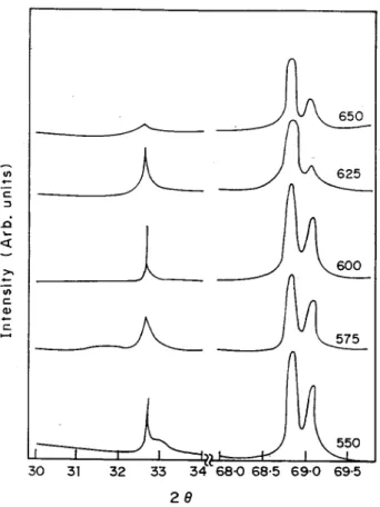
Figure 2. X-ray diraction pattern of the CaF2 lm
an-nealed at temperatures ranging from 550o to 650oC. It has also been observed by Perez et al [11] that the lms obtained by low energy cluster beam deposi-tion technique contain large clusters of the host mate-rial which do not fragment on the substrate leading to a random substrate \pavement" and orient themselves to a suitable ordering with the substrate. The clusters subsequently diuse and coalesce with other clusters or would remain as separate entity depending on their size. It is expected therefore, that during post anneal-ing the clusters will gain some kinetic energy (obtained from thermal energy) and hence fragment and thereby the original orientation will be disturbed. However, at
lower annealing temperature all the clusters may not fragment and re-orient themselves which would result in the decrease in FWHM. As the annealing temper-ature increases, more and more clusters fragment and re-orient showing optimum activity at 650oC. The opti-mum temperature could be expected to depend on the nature of the substrate and also on the type of mate-rial deposited. A further increase in the temperature, beyond the optimum, would be expected to result in surface to lm reaction reducing the crystallinity. It was also observed that the substrate temperature at-tained during the deposition (due to the heat recieved from the crucible source) was close to the optimum an-nealing temperature.
Figure 3. X-ray diraction pattern of the as-deposited CaF2
lm.
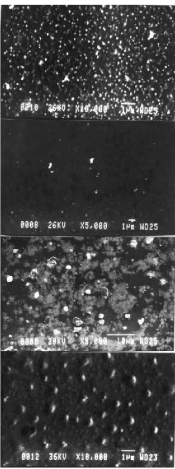
Figure 4. SEM photographs of a) lm annealed at 600oC;
b) lm annealed at 650oC; c) lm annealed at 700oC; d)
as-deposited lm.
Figure 5. Frequency vs Capacitance plot of the Metal/CaF2/Metal structure.
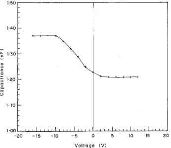
To as certain the usefulness of the CaF2 interlayer for superconductor lms used in microwave applications C-V measurements were carried out. Fig. 5 shows the frequency Vs capacitance characteristics of CaF2 lms in the form of Metal-Insulator-Semiconductor struc-ture. The capacitance is found to saturate at higher fre-quencies as expected for a MIS structure. Fig. 6 shows the capacitance-voltage measurements carried out at 1Mhz frequency for the lms annealed at optimumtem-perature of 650oC and the as-deposited lm. The total capacitance C of the MIS diode could be represented [12] as a series combination of the insulator capacitance C
iand the semiconductor depletion layers capacitance C
j. Hence,
C=C i
C j
=(C i+
C j)
The total capacitance is seen to decrease with the in-creasing forward voltage while the surface is depleted of charges. When the applied voltage is reversed ac-cumulation of holes at the semiconductor surface takes place. As a result, the total capacitance is close to the insulator capacitance
i
=dwhere
con-stant of the lm annealed at optimum temperature is as high as 18.
Figure6. C-V plot ofthe Metal/CaF 2
/Metal structure at 1MHz.
IV Conclusion
Good quality c-axis oriented CaF
2 buer layers on Si were grown using the low energy cluster beam deposi-tion technique. As-deposited lm were found to ensure a good surface morphologyand better crystallinity than the post annealed lms. The dielectric constant of the as-deposted lms is of the order of 2.01 which is in close agreement with the reported values.
References
1. O.W. Kwon, B.W. Langlew, R.F.W. Pease, M.R. Beasley, EEE Electron Devices Lett. EDL-8, 582, (1987).
2. W. Hartwig, C. Passov, Applied Superconductiv-ity, Edited by V.L. Newhouse (Academic Press, New York) Vol ii p542.
3. G. Koren, E.Polturak, B. Fisher, D. Cohen and G. Kimel, Appl. Phys. Lett. 53, 2330 (1988). 4. T. Venkatesan, E.W. Chase, X.D. Wu, A. Inam,
C.C. Chang, F.D. Shokoohi, Appl. Phys. Lett. 53, 243 (1988).
5. R.P. Lowndess, J. Phys C.2, 1595 (1969). 6. H. Ishiwara, T. Asano, Appl. Phys. Lett. 40, 66
(1982).
7. A.N. Tiwari, S. Blunier, H. Zogg, J. Appl. Phys. 71, 10 (1992).
8. Susumu Horita, M. Murakawa, T. Fujiyama, Jpn. J. Appl. Phys. 34, 1942 (1995).
9. J. Bohandy, E. Agostinelli, B.F. Kim, W.J. Green, T.E. Phillips, F.J. Adrian, K. Moorjani, J. Appl. Phys. 65, 4147, (1989).
10. S.S. Bhagwat, A.R. Bhangale, J.M. Patil, V.S. Shirodkar, Ramprasad, N.C. Soni, Proc. Int Con. Vac. Sci and Tech., CAT Indore, Vol 2, pp 345 (1995).
11. A. Perez, P. Melinon, V. Paillard, V. Dupuis, P. Jensen, A. Hoareau, J.P. Perez, J. Tuaillon, M. Broyer, J.L. Vialle, M. Pellarin, J. Lerme, Nanos-tructured Materials,34, 43 (1995).
12. S.M. Sze,Physics of Semiconductor Devices, 2nd ed., pp 371 (1981).