Ricardo Jorge Barros Fitas
Licenciado em Ciências daEngenharia Eletrotécnica e de Computadores
Study of a Time Assisted SAR ADC
Dissertação para obtenção do Grau de Mestre em
Engenharia Electrotécnica e de Computadores
Orientador: Nuno Filipe Silva Veríssimo Paulino, Prof. Doutor, Universidade Nova de Lisboa
Júri
Presidente: Prof. Doutor Paulo da Costa Luís da Fonseca Pinto, FCT-UNL Arguente: Prof. Doutor João Carlos da Palma Goes, FCT-UNL
Study of a Time Assisted SAR ADC
Copyright © Ricardo Jorge Barros Fitas, Faculdade de Ciências e Tecnologia, Universidade NOVA de Lisboa.
inves-A c k n o w l e d g e m e n t s
First of all, I would like to start thanking Prof. Nuno Paulino for his support, commitment, patience and motivation to find new approaches to problems which kept emerging. I would also like to show my gratitude to all the other Professors at DEE FCT-UNL who, despite not having the resources most of them would like and deserve to have, do their best on a daily basis to pass their knowledge and experience.
My friends and colleagues cannot be forgotten. Many interesting discussions and moments of fun and laughter were certainly some of the best I had so far.
A b s t r a c t
The demand for low power systems has been increasing in recent years and Analog-to-Digital Converters (ADCs) are key blocks of many of these systems as they convert a physical quantity into the digital domain so that this information can be further processed or stored using digital techniques.
Data Converters based on Charge Redistribution using of Successive Approximation Registers (SAR) are becoming one of the most popular ADC architectures for moderate speed, medium resolution and low power applications. Due to their low analog complex-ity SAR ADCs benefit from technology scaling. However, this scaling often comes with a supply voltage reduction and the noise levels do not decrease at the same rate, which translates into a performance decrease. Therefore, new opportunities emerge to explore other physical quantities such as time, frequency, phase or charge in the circuit.
This thesis focuses on studying how the time domain information can be used to increase the performance of SAR ADCs. To do so, a new SAR ADC architecture is pro-posed in which a Time-to-Digital Converter (TDC) is used to convert the time domain information, provided by the comparator, into the digital domain. This new architecture was modelled in MATLAB as a 12 bit TDC assisted SAR ADC, using information from electrical simulations of the comparator and the TDC, designed in Cadence in 65 nm ST Microelectronics CMOS technology.
Simulation results demonstrated that, to achieve a better performance when compared to more traditional SAR structures, the TDC energy and latency should be minimized. Another limiting factor was the large voltage range in which only 1 bit could be extracted from the time-to-voltage conversion by the TDC due to the comparator’s fast response in this range. The proposed architecture was also extended to incorporate aBypass Window
in the time domain, which allowed to substantially decrease the number of clock cycles necessary to solve the 12 bits of the ADC.
R e s u m o
A procura por sistemas de baixa potência tem vindo a aumentar e os Conversores Analógico-Digitais (ADCs) são blocos-chave de muitos desses sistemas, dado que convertem uma quantidade física para o domínio digital, para que essa informação possa ser processada digitalmente.
Os conversores baseados em Redistribuição de Carga, utilizando Registos de Aproxi-mações Sucessivas (SAR), estão a aumentar a sua popularidade, sendo uma das arquitetu-ras mais populares atualmente. Devido à sua baixa complexidade analógica, os converso-res SAR beneficiam do escalamento da tecnologia que vem muitas vezes associado a uma redução da tensão de alimentação, e tendo em conta que os níveis de ruído não diminuem na mesma medida, isto traduz-se numa diminuição do desempenho. Deste modo, surgem novas oportunidades para explorar outras quantidades físicas, como tempo, frequência, fase ou carga nos circuitos.
Esta tese tem como objetivo o estudo de como a informação no domínio do tempo pode ser utilizada para aumentar o desempenho dos conversores SAR. Para isso, é proposta uma nova arquitetura de um ADC, na qual um Conversor Tempo-para-Digital (TDC) é usado para converter a informação do domínio do tempo, fornecida pelo comparador, para o domínio digital. Esta nova arquitetura foi modelada em MATLAB como um SAR ADC de 12 bits assistido por um TDC, utilizando resultados de simulação de circuitos projetados na tecnologia CMOS 65 nm da ST Microelectronics.
Os resultados da simulação demonstraram que, para se obter um melhor desempenho quando comparado com estruturas SAR mais tradicionais, a energia e a latência do TDC devem ser minimizadas. Outro fator limitador é a grande gama de tensão na qual somente 1 bit pode ser extraído da conversão de tempo para tensão pelo TDC devido à rápida resposta do comparador nesta gama. A arquitetura proposta foi, ainda, modificada de modo a incorporar uma janela de Bypasso que permitiu diminuir substancialmente o número de ciclos de relógio necessários para resolver os 12 bits do ADC.
C o n t e n t s
List of Figures xiii
List of Tables xv
Acronyms xvii
1 Introduction 1
1.1 Motivation and Background . . . 1
1.2 Original Contributions . . . 2
1.3 Thesis Organization . . . 3
2 Analog-to-Digital Conversion Fundamentals 5 2.1 Sampling . . . 6
2.1.1 Nyquist-Shannon Criterion . . . 8
2.2 Quantization . . . 8
2.3 Performance Metrics . . . 10
3 Analysis of SAR ADCs 11 3.1 SAR ADC Block Diagram . . . 11
3.1.1 Successive Approximation Algorithm . . . 12
3.1.2 SAR ADC Sub-Blocks . . . 12
3.2 SAR ADCs Power . . . 15
3.3 SAR ADCs Switching Schemes . . . 15
3.3.1 Conventional Switching Scheme . . . 16
3.3.2 Merged Capacitor Switching (MCS) or Vcm-based Switching Scheme 24 3.4 Other SAR Architectures . . . 25
4 Time-to-Digital Converters 27 4.1 Counter Based TDC . . . 27
4.2 Delay-Line Based TDC . . . 28
4.3 Sub-Gate Delay Resolution TDCs . . . 29
4.3.1 Vernier Delay-Line TDC . . . 29
CO N T E N T S
5 Proposed Architecture 33
5.1 System Level Description . . . 33
5.2 High-Level Model - Single Ended . . . 34
5.3 CMOS Circuits Implementation . . . 42
5.3.1 Comparator . . . 42
5.3.2 Time-to-Digital Converter . . . 44
5.3.3 Comparator and TDC . . . 47
5.4 High-Level Model - Fully Differential . . . . 49
5.4.1 Energy . . . 53
6 Conclusions and Future Work 57 6.1 Conclusions . . . 57
6.2 Future Work . . . 59
Bibliography 61
L i s t o f F i g u r e s
1.1 Conventional SAR ADC Architecture. . . 2
2.1 Ideal mathematical model of the Analog-to-Digital conversion process. . . . 5
2.2 Sampling process in the time domain. . . 6
2.3 Sampling process in the frequency domain. . . 7
2.4 Aliasing effect. . . . 8
2.5 Ideal Quantizer characteristic. . . 9
2.6 Frequency Spectrum . . . 9
3.1 Conventional SAR Architecture with Sample-and-Hold Circuit - single ended. 11 3.2 Flow Diagram of the Successive Approximation Algorithm. . . 13
3.3 Conventional 3 bit SAR ADC architecture - differential circuit schematic. . . 16
3.4 Conventional 3 bit SAR ADC switching procedure. . . 17
3.5 10 bit SAR ADC switching energy as a function of the output code - conven-tional switching scheme. . . 24
3.6 3 bit SAR ADC Vcm-based architecture - differential circuit schematic. . . . 24
3.7 3 bit SAR ADC Vcm-based switching procedure. . . 25
3.8 10 bit SAR ADC switching energy as a function of the output code - Vcm-based switching scheme. . . 26
4.1 Counter Based TDC principle of operation. . . 28
4.2 Delay-Line Based TDC Architecture. . . 28
4.3 Vernier Delay-Line TDC Architecture. . . 30
4.4 Operating principle of Vernier Delay-Line TDC. . . 30
5.1 Proposed Architecture - Single Ended. . . 33
5.2 Simulation results of the comparator - Comparator’s decision timevs∆V in. . 35
5.3 Comparator’s decision time and TDC output codevs∆V in. . . 36
5.4 Number of bits decided by the TDCvs∆V in. . . 37
5.5 System’s digital output codevsVin - the two lines are overlap. . . 38
5.6 System’s DNL and INL. . . 39
5.7 Number of comparisonsvsVin. . . 39
L i s t o f F i g u r e s
5.9 System’s digital output codevsVin. - the two lines are overlap. . . 40
5.10 System’s DNL and INL. . . 41
5.11 Number of comparisonsvsVin. . . 41
5.12 Percentage of comparisons. . . 41
5.13 Comparator Circuit, as proposed in [42]. . . 43
5.14 Single Comparison -∆V in= 10mV , V cm= 450mV , Load= 20f F . . . . 43
5.15 Differential Time to Digital Converter Circuit. . . . 45
5.16 SR Latch to be used asearly-late detector. . . 45
5.17 TDC response for a 10 ps interval between theSTARTandSTOPsignals. . . 46
5.18 Comparator’s decision time and TDC output codevs∆V in. . . 47
5.19 Latencyvs∆V in. . . 48
5.20 Energyvs∆V in. . . 48
5.21 Proposed Architecture - Fully Differential. . . . . 49
5.22 Number of bits decided by the TDCvs∆V in. . . 51
5.23 System’s digital output codevsVin. - the two lines are overlap. . . 51
5.24 System’s DNL and INL. . . 52
5.25 Number of comparisonsvsVin. . . 52
5.26 Percentage of comparisons. . . 52
5.27 Conversion timevsVin. . . 53
5.28 Conventional Architecture and Proposed Architecture using the Conventional Switching schemevsVin. . . 54
5.29 Vcm-based Architecture and Proposed Architecture using the Vcm-based Switch-ing schemevsVin. . . 54
5.30 Charge Sharing Architecture and Proposed Architecture using the Charge Sharing Switching schemevsVin. . . 55
L i s t o f Ta b l e s
3.1 Comparison of DAC switching schemes for 10 bit SAR ADCs considering the
Conventional switching method as the reference. . . 15
5.1 Lookup Tableto be used by theCoarseConverter. . . 37
5.2 Comparator transistor sizes. . . 44
5.3 Transistor sizes of the inverters used to implement the delay lines. . . 45
5.4 SR Latch transistor sizes. . . 46
A c r o n y m s
ADC Analog-to-Digital Converter.
CR Charge Redistribution. CS Charge Sharing.
DAC Digital-to-Analog Converter. DNL Differential Non-Linearity.
ELD Early-Late Detector.
INL Integral Non-Linearity.
LSB Least Significant Bit.
MCS Merged Capacitor Switching. MSB Most Significant Bit.
SAR Successive Approximation Register. SNR Signal-to-Noise Ratio.
C
h
a
p
t
e
r
1
I n t r o d u c t i o n
1.1 Motivation and Background
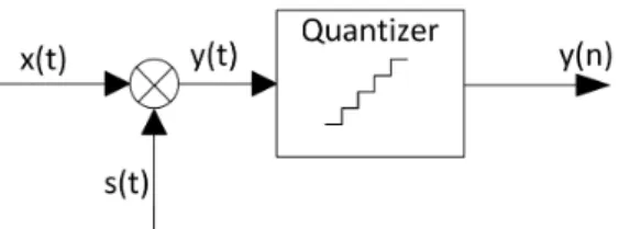
The need for low power devices has been increasing in recent years. This trend is still continuing as the need for portability is increasing, as well as the need for newer im-plantable medical devices [1], hence long battery life is becoming a requirement for today’s electronic systems. Analog-to-Digital Converters (ADC) are key blocks of these systems as they sample a physical quantity and convert into the digital domain so that this information can be further processed or stored using digital techniques.
Successive Approximation Register (SAR) ADCs, based on Charge Redistribution (CR) on weighted capacitors [2] techniques, have arisen among other ADC architectures for moderate speed, medium-resolution [3] and very low-power applications, while keeping analog simplicity [1]. The traditional SAR structure, shown in Figure 1.1, consists of a sample-and-hold circuit embedded in the DAC, a comparator, a digital-to-analog con-verter (DAC) and a control logic block which implements the binary search algorithm. This binary search algorithm requires N clock cycles for a N-bit SAR ADC. This translates into N comparator decisions which are a major source of power consumption in SAR ADCs and the bottleneck for SAR’s throughput. Additionally, power in the capacitive ar-rays, in the case of a capacitive DAC, is wasted if the signal does not fall within the desired range. This is because the switching energy of the DACs is proportional toCV2, hence keeping the unit capacitors small is important to keep the power consumption low. How-ever, using very small unit capacitors degrades the matching between capacitors which will degrade the non-linearity parameters of ADCs, namely Integral Non-Linearity (INL) and Differential Non-Linearity (DNL). This means that the size of the unit capacitor must
be chosen by making a trade-offbetween the kT
C noise requirements, capacitor matching
C H A P T E R 1 . I N T R O D U C T I O N
mainly constituted by digital circuits, SAR ADCs benefit from technology scaling, hence a better performance is expected in terms both speed of operation and power consumption because the parasitics are decreased [1]. Moreover, since no complex analog circuitry such as operational amplifiers are used in SAR ADCs and no large voltage swings are required, unlike in other ADC architectures, SAR ADCs are more suitable to operate at low supply voltages, which also contributes to its low-power operation [5].
SAR Logic ΦClock
Vin
DAC
Sample-and-Hold
VSH
VDAC
VREF
Figure 1.1: Conventional SAR ADC Architecture.
However, with the technology scaling and the supply voltage reduction, the design of analog circuits in CMOS technologies is becoming more challenging, as keeping the transistors working in saturation and still maintaining a sufficient signal swing becomes
critical, while the noise levels do not go down with decreasing supply voltage. This translates into a direct decrease of the Signal-to-Noise Ratio (SNR) which will severely reduce the performance of the ADCs. That being said, new opportunities arise for using new physical quantities such as time, charge, phase or frequency instead of traditional quantities such as voltage and current in the circuits. In this sense, and bearing in mind that digital circuits benefit from technology scaling [6], it is interesting to study how these domains can be used to increase the performance of ADCs.
1.2 Original Contributions
The main purpose of this thesis is to study how the time domain information can be used to assist the commonly used successive approximation algorithm in SAR ADCs in order to achieve a better performance.
Considering the SAR ADC architecture, the time a comparator takes to perform a decision is directly related with its input signals. This means that extra information can be extracted if this time is measured using, for example, a Time-to-Digital Converter (TDC) [7]. By measuring the time at which the comparator output changes and using this information to select the DAC code in the SAR structure closer to the final ADC output code, several bits can be decided at once, hence power is saved both in the number of comparator decisions needed and in the DAC switching because no wrong steps are made in the bits decided by the TDC. Moreover, since several bits are decided at once, it is also possible to increase SAR’s throughput [8]. By using such architecture, it is expected
1 . 3 . T H E S I S O R GA N I Z AT I O N
that the performance of the system increases with technology scaling since most of the complexity is transferred to the digital domain. For this reason, the proposed circuits will be developed in a 65nm ST Microelectronics CMOS Technology and their characteristics included in the MATLAB high-level models of the proposed converter.
Since very low-power ADCs are crucial for implantable medical devices, this structure intends to be an alternative to the ADCs used nowadays for this applications.
1.3 Thesis Organization
This thesis is organized in 6 chapters, starting with this introductory one. Chapter 2 explores the fundamentals of Analog-to-Digital conversion, both in time and frequency domains. These concepts are critical when designing data converters since they limit the
Fin
Fs
ratio, therefore frequency spacing between spectral components, and the in-band quantization noise.
The third chapter presents the principles behind SAR ADCs. The successive approx-imation algorithm is explained and the function of each circuit block is discussed. For each block, non-idealities are presented and circuit techniques to overcome such prob-lems are proposed. The power consumption of these constituting blocks is studied in detail in order to improve the performance of these converters. Two different DAC
switch-ing schemes, which implement the successive approximation algorithm, are analysed in detail. Also, a comparison among these and other switching methods is made. Finally, recent SAR ADCs operating outside their traditional application spaces or with different
architectures are briefly presented.
Time-to-Digital Converters are key components to convert the time domain informa-tion into the digital domain. In this sense, Chapter 4 focuses on the fundamentals of these converters, architectures and how to obtain sub-gate resolution in TDC circuits.
In Chapter 5, the proposed architecture, in which a TDC is introduced into the tradi-tional SAR ADC architecture, is presented and explained. High-level MATLAB models of the proposed converter and the circuits implemented in 65 nm CMOS ST Microelectron-ics, along with electrical and system level simulations, can also be found in this chapter.
C
h
a
p
t
e
r
2
A n a l o g - t o - D i g i t a l C o n v e r s i o n
F u n d a m e n t a l s
The signal conversion (in ADCs) corresponds to the transformation of a analog input signal into a digital output signal. However, an analog signal has an infinite number of values in a finite time interval. As result, it is necessary to periodically sample the input signal. After the signal is sampled, it is then quantized so that a finite (digital) value can be assigned to the sampled signal and the analog to digital conversion is finished. The conversion procedure is then repeated until enough data is collected to perform the action demanded by the target application. It is also important to refer that the conversion algorithm depends on the converter’s architecture, which is not the subject of this chapter. Instead, this chapter focuses in understanding the conversion process at a system level, as shown in Figure 2.1. Therefore, a brief mathematical approach to the sampling and quantization theories will be presented. Finally, some useful metrics to characterize converters will be presented.
C H A P T E R 2 . A N A LO G -TO - D I G I TA L CO N V E R S I O N F U N DA M E N TA L S
2.1 Sampling
Sampling is the procedure of transforming a time-continuous signal,x(t)1, into a time-discrete signal. The sampling function,s(t), is a sequence ofdiracpulses equally separated by a time period Ts, defined as Ts = 1
Fs
, where Fs is the sampling frequency, therefore
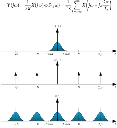
s(t) can be written as Eq. 2.1. In this sense, the sampled signal, y(t), can be defined as Eq. 2.2, [3]. Figure 2.2 is representative of the sampling process in the time domain.
s(t) =
+∞
X
n=−∞
δ(t−nTs) (2.1)
y(t) =x(t)·s(t) =
+∞
X
n=−∞
x(t−nTs) (2.2)
Figure 2.2: Sampling process in the time domain.
In order to analyse the impact of this operation in the frequency domain, Eq. 2.1 can be transformed into Eq. 2.3 by taking its Fourier Transform. Since Eq. 2.1 represents
1x(t) is assumed to be a band limited signal with a bandwidth fromf= 0 Hz tof= BW Hz.
2 . 1 . SA M P L I N G
a periodic pulsed signal in the time domain, its Fourier Transform is simply a periodic pulsed signal in the frequency.
S(jω) =2π
Ts +∞
X
k=−∞
δ jω−jk2π Ts
!
(2.3)
In the frequency domain, Eq. 2.2 can be rewritten as Eq. 2.4 since a multiplication in the time domain is evaluated as a convolution in the frequency domain [9]. The sampling mechanism in the frequency domain is illustrated in Figure 2.3.
Y(jω) = 1
2πX(jω)⊗S(jω) =
1
T s
+∞
X
k=−∞
X jω−jk2π Ts
!
(2.4)
Figure 2.3: Sampling process in the frequency domain.
By observing the frequency spectrum ofY(jω) in Figure 2.3, it is evident what Eq. 2.2 and Eq. 2.4 state: by sampling a signal with a train ofdiracpulses equally separated by a time periodTs, an infinite number of replicas of the original signal spectrum (X(jω)) is
created in the frequency spectrum, theseimagesof the sampled signal centred at multiples ofFs[3, 9], as shown in the frequency spectrum ofY(jω) in Figure 2.3.
As a consequence of this phenomenon, if the time difference between two adjacent
samples, i.e. Ts, is too high, the spectral components of the sampled signalY(jω) will
overlap. This phenomenon is known asaliasingand it is shown in Figure 2.4. Thealiasing
effect produces a mixing of sampled data in the frequency domain and the original signal
can no longer be recovered. Hence, in order to avoid it, theNyquist-Shannon Criterion
C H A P T E R 2 . A N A LO G -TO - D I G I TA L CO N V E R S I O N F U N DA M E N TA L S
Figure 2.4: Aliasing effect.
2.1.1 Nyquist-Shannon Criterion
TheNyquist-Shannon Criterion was formulated in 1923 by Harry Nyquist [10] and ex-tended in 1948-49 by Claude Shannon [11, 12] and states: a sampled signal can be recov-ered with no loss of information if the sampling frequencyFsis, at least, two times higher than the maximum signal frequencyBW[3, 9]. The sampling frequency which satisfies this condition is known as the Nyquist Frequency,fN, and is defined as Eq. 2.5.
Fs=fN= 2·BW (2.5)
In order to clean the frequency spectrum so that only the baseband component is present, a low pass filter is used. According to what was previously demonstrated, the larger the sampling frequency the more separated are the spectral components, thus the more relaxed are the low pass filter requirements [3].
It is also worth mentioning that ADCs which work close to the Nyquist Frequency are known as theNyquist Converters. Another family of ADCs, which work at much higher frequencies thanfN are calledOversampling Convertersbut these are out of the purpose
of this thesis.
2.2 Quantization
After the analog signal has been sampled, next step in the analog to digital conversion process is the quantization of the signal’s physical quantity so that a digital value can be assigned to that sample. The digital representation of the signal depends on the number of bits N at the output, as well as on the full scale range FS of the quantizer. Knowing these two parameters, it is possible to define the value of theLeast Significant Bit(LSB), ∆, as Eq. 2.6.
∆=FS
2N (2.6)
In Figure 2.5 the characteristic of an ideal quantizer is presented for an ideal 3 bit quantizer, corresponding each step size to one ∆. According to this characteristic, all input values will be encoded to the corresponding output code.
2 . 2 . Q UA N T I Z AT I O N
Figure 2.5: Ideal Quantizer characteristic.
However, since∆ is not infinitely small (since the number of bits N is not infinite), there will always be some error introduced by the quantization process, theQuantization Error,qe. From Figure 2.5, it is possible to observe that the quantization error depends on the input signal and has a maximum error of
∆
2
. Nevertheless, if it is assumed that the input signal is rapidly changing such thatqeis considered a random variable uniformly distributed between±
∆
2, the probability density function of the quantization error in this range is also assumed to be constant and uniformly distributed. Under these conditions, the quantization error can be treated as white noise [3, 9]. Thus, theQuantization Noise
power can be calculated from Eq. 2.8Pqe in theNyquist Bandwidth.
Pqe=
1 ∆
Z ∆/2
−∆/2
q2e dqe=
∆2
12 (2.7)
IfFsis higher than that in the conditions of Eq. 2.5, Eq. 2.7 can be extended to Eq. 2.8.
Pqe=
∆2
12· 2BW
Fs
(2.8) According to Eq. 2.8, the quantization noise power can be reduced, in the signal bandwidth, both by increasing the quantizer’s resolution and increasing the sampling frequency [3]. While increasing the quantizer’s resolution decreases the quantization error, hence it’s power, increasingFs will result in the quantization noise power being
spread through a wider frequency range, therefore its effect becomes smaller inside the
band of interest, as shown in Figure 2.6.
C H A P T E R 2 . A N A LO G -TO - D I G I TA L CO N V E R S I O N F U N DA M E N TA L S
2.3 Performance Metrics
The performance of every data converter is generally categorized according to several metrics, both dynamic and static. This section intends to summarize these metrics.
TheSignal-to-Noise Ratio(SNR) stands for the ratio of the input signal power to the quantization noise power. The SNR can be further extended to incorporate the power of all the unwanted frequency components. In this case, it should be named Signal-to-Noise-and-Distortion Ratio(SNDR).
Having a large SNDR usually translates into large aEffective Number of Bits(ENOB) and largeTotal Harmonic Distortion(THD). The THD is defined as the ratio of the sum of the power of all the signal harmonics higher than the first to the power of the first harmonic. These harmonics usually limit theSpurious Free Dynamic Range(SFDR), since it is a metric of the distance between the signal and the largest unwanted frequency com-ponent. Another important parameter when categorizing data converters is theDynamic Range(DR), which defines the range of signal amplitudes in which the converter is able to operate. It is limited by the thermal noise, at low signal amplitudes, and by distortion and jitter, at higher signal amplitudes. These are dynamic performance metrics as they relate to the frequency behaviour of the converter.
The Differential Non-Linearity (DNL) and Integral Non-Linearity (INL) are linearity measures which specify the converter’s step difference from an ideal LSB size and its
input-output deviation from an ideal conversion curve, respectively. These are static metrics since they are obtained by slowly sweeping the converter’s input over its full-scale range.
TheWalden Figure of Merit (FoM) is a performance metric useful when comparing different data converters and it is formulated in Eq. 2.9. It takes into account the amount
of power the converter needs to achieve a certain performance, expressed by theEffective Number of Bits, over a certain input signal frequency bandwidth,BW. The Figure of Merit is expressed in units ofjoules per conversion step, hence the lower FoM obtained, the better the converter’s performance.
FoM= Power
2EN OB×2BW (2.9)
C
h
a
p
t
e
r
3
A n a ly s i s o f SA R A D C s
The popularity of SAR ADCs has been increasing throughout the last years for moderate-speed, medium-resolution [3] mainly due to their exceptional energy-efficiency [13]. This
is accomplished because their analog complexity is kept low, hence SAR ADCs benefit from technology scaling [1, 14]. In this sense, the present chapter aims to study the principle of operation of this ADCs and to explore different SAR architectures reported
in the literature.
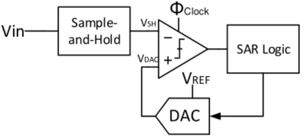
3.1 SAR ADC Block Diagram
The conventional SAR ADC architecture is depicted in Figure 3.1. It comprises a sample-and-hold circuit, a comparator, a DAC and control logic block [2] that implements the successive approximation algorithm.
SAR Logic ΦClock
Vin
DAC
Sample-and-Hold
VSH
VDAC
VREF
Figure 3.1: Conventional SAR Architecture with Sample-and-Hold Circuit - single ended.
The first step towards a full conversion in this kind of ADCs is sampling the input signal using the sample-and-hold circuit,VSH. Afterwards, the control logic block tries
C H A P T E R 3 . A N A LYS I S O F SA R A D C S
the DAC data input bits, one at a time, starting from the Most Significant Bit (MSB) and moving towards the LSB. Once all the bits are decided, the conversion is finished. The approximation method implemented by the control logic block is based on a binary search algorithm, known as theSuccessive Approximation Algorithm[3].
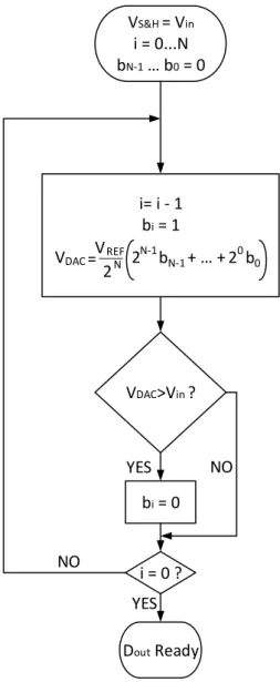
3.1.1 Successive Approximation Algorithm
The Successive Approximation Algorithm implemented by the control logic block is rep-resented in the flow diagram of Figure 3.2 for anN-bit SAR ADC. In the beginning, all the feedback DAC data input bits (bN−1to b0) are set to ZERO. Then, the control logic
block sets the MSB (bN−1) of the DAC to ONE and the digital word is converted intoVDAC.
Afterwards, the comparator present in the SAR ADC architecture evaluates ifVDAC is
greater than VSH. If that is the case,bN−1 is set back to ZERO, otherwise it is kept at
ONE. This process is repeated until all bits are determined. According to this, aN-bit SAR ADC requiresN+ 1 clock cycles to perform a full conversion [3].
3.1.2 SAR ADC Sub-Blocks
Each block in the SAR structure has a very specific function and its implementation strongly affects the performance of the converter. Therefore, this section intends to
provide an overview of their implementation and present some design tradeoffs.
3.1.2.1 Sample-And-Hold
Ideally, this block should be able to acquire a sample of the signal without any interference. However, since this circuits generally consist of a switch and a capacitor to hold the sampled value, both components can affect the sampled signal.
The sampling capacitor,Chold, for example, will also sample some noise along with
the signal. For this reason, the sampling capacitor size should be chosen so that it re-spects the noise requirements, kT
Chold. However, a big capacitor translates into large time
constants [3].
The switch implementation should also be as linear as possible, which is not achiev-able by using only one transistor. Such a simple implementation presents aRON which
varies with the input signal value, thus introducing distortion [3].Transmission gatesare often used to decrease the effectiveRON by usingN MOS andPMOS devices in
paral-lel and the signal related distortion effect can be overtaken by using techniques such as
bootstrapping[15].
Moreover,Charge Injectioneffects occur due to the ON/OFF operation of the switching
procedure. Half of the charge in the channel of the MOS switches during the OFF transi-tion will be absorbed byChold. Likewise, MOS transistors absorb charge to be turned on. Again, the charge stored inCholdwill be modified and the sampled signal value altered.
3 . 1 . SA R A D C B LO C K D I AG R A M
VDAC>Vin ?
bi = 0
i = 0 ?
Dout Ready
YES
YES NO
NO
VS&H = Vin
i = 0...N bN-1 b0 = 0
=V VDAC ____REF
2N 2
N-1
bN-1+ + 2 0
b0
i= i - 1 bi = 1
Figure 3.2: Flow Diagram of the Successive Approximation Algorithm.
The resulting circuit is no longer a simple circuit constituted by a switch and a capac-itor. Also, using all these circuit techniques can translate into a large power consump-tion [3]. However, in Charge Redistribuconsump-tion SAR ADCs, the Sample-and-Hold funcconsump-tion can be embedded in the (capacitive) DAC, therefore resulting in a much more energy-efficient solution [2, 14, 16].
3.1.2.2 Comparator
The comparator is the only active block in a SAR ADC. It compares the sampled signal
VSH with the DAC voltageVDAC and its decision is used by the SAR Control Logic to
perform the successive approximation algorithm [3].
C H A P T E R 3 . A N A LYS I S O F SA R A D C S
resolve very small voltage differences, at leastVLSB/2, within a reasonable amount of time.
Since the comparator’s decision time is directly related to the signals under comparison, this time domain information can be used to extract information from the amplitude domain [7], as will be done in this work.
Besides accuracy and speed,kickback noiseandoffsetshould also be taken into account. Whileoffsetis only translated in a deviation in the ADC’s conversion curve, hence does not degrade the linearity metrics of the ADC (DNL and INL),kickback noisemay cause a wrong decision by the comparator if its amplitude is too high. Therefore, comparator architectures in which the output stage is separated from the input stage are preferred since it helps both in decreasing the kickback and the input referred offset [3, 17].
3.1.2.3 SAR Control Logic
This block is responsible for implementing the binary search algorithm described in 3.1.1. More advanced switching algorithms allow to save power related to DAC switching and this is a subject under study in this work. This block, besides demanding some power to operate at reasonable speeds, benefits from technology scaling since it is mainly consti-tuted by digital circuits.
3.1.2.4 Digital-to-Analog Converter
In SAR ADCs, the feedback DAC is used to produce a voltage as close as possible to the input voltage and it can be considered the most important block in a SAR ADCs since, together with the Sample-and-Hold circuit, the feedback DAC determines the overall linearity of the converter [3]. Moreover, the DACsettling timeplays an important role in determining the maximum conversion speed. Nevertheless, enough time should be given so thatVDAC settles within half LSB [16]. If the comparator starts making a decision
before the DAC is fully settled, a wrong decision may occur, hence the final output code will be incorrect if no correction methods are used [1].
Several types of DACs can be used in SAR ADCs, however charge domain DACs are the most suitable for low-power SAR ADCs due to their zero static power consumption [3, 4]. Moreover, capacitive DACs based on charge redistribution can provide inherent Sample-and-Hold function, as previously mentioned. Charge Sharing (CS) DACs are an alterna-tive to Charge Redistribution architectures. Depending on its structure, CS DACs can be more energy-efficient than CR based DACs, however they need an auxiliary sampling
capacitor and the performance reported in recent works does not match that possible with CR DACs [18]. For this reasons, emphasis will be given to DACs operating in the charge domain using charge redistribution schemes .
Considering a capacitive DAC, the power consumption depends on the switching method employed and the total capacitance of the capacitive array, hence keeping the unit capacitors small is important to keep the power consumption low. However, decreasing the value of the unit size capacitor degrades the matching between capacitors, which will
3 . 2 . SA R A D C S P OW E R
have a direct impact in the converter’s linearity. Also, the kT
C noise requirements should
be respected. This means that the unit size capacitor must be chosen by making a tradeoff
between power consumption, capacitor matching and noise requirements [3, 4].
3.2 SAR ADCs Power
Charge Redistribution SAR ADCs are capable of achieving very high energy-efficiency [13,
16], being most of the energy consumed by the comparator, the DAC switching and the digital circuits in the Control Logic block [14].
The comparator power depends on the number of comparisons performed, which increases with the resolution of the ADC, thus the comparator power can not be reduced without reducing the number of comparisons necessary.
As mentioned before, digital circuits benefit from technology scaling [6] so, in or-der to increase SAR ADCs energy-efficiency even more, more advanced DAC structures,
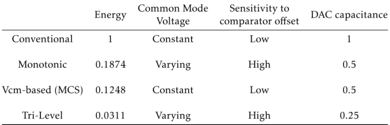
namelyCapacitive Array with Attenuation Capacitor [19] andSplit Capacitor Array[20], and switching algorithms such as theEnergy Saving[21],Monotonic[22, 14],Merged Ca-pacitor Switching (MCS)[23] orVcm-based[16], orTri-Level [24] must be used. Table 3.1 summarizes the DAC switching schemes, according to [18].
Table 3.1: Comparison of DAC switching schemes for 10 bit SAR ADCs considering the Conventional switching method as the reference.
Energy Common Mode Voltage
Sensitivity to
comparator offset DAC capacitance
Conventional 1 Constant Low 1
Monotonic 0.1874 Varying High 0.5
Vcm-based (MCS) 0.1248 Constant Low 0.5
Tri-Level 0.0311 Varying High 0.25
3.3 SAR ADCs Switching Schemes
Several Switching schemes were developed throughout the last years in order to minimize the energy required by the DAC transitions. In this thesis, only the fully differential
implementation of the Conventional and the MCS schemes will be explored in detail, since the other switching methods lead to a variation of the common-mode voltage, hence can not be used in the architecture proposed in Chapter 5.
It should be mentioned that fully differential implementations provide common mode
C H A P T E R 3 . A N A LYS I S O F SA R A D C S
3.3.1 Conventional Switching Scheme
The Conventional Switching scheme, proposed in [2], is based on the trial and error algorithm presented in 3.1.1. Figure 3.3 depicts a conventional 3 bit fully differential SAR
ADC structure. Since this ADC is fully differential, only the positive side of the ADC
operation will be described, as the operation on the other side is complementary.
SAR Logic
Vin Vref
4C 2C C C
4C 2C C C
VrefVip
Vcm Vcm
Dout B B B2 1 0
Figure 3.3: Conventional 3 bit SAR ADC architecture - differential circuit schematic.
The conversion starts with the sampling phase,φS. At the sampling phase, the bottom
plates of the capacitor network are connected toVip and the top plates are connected to
the common mode voltage,Vcm. Next, the bottom plate of the MSB capacitor is switched to the reference voltage,Vref, and the bottom plates of the other capacitors on the positive
DAC array switched to ground,gnd. On the negative array, the complementary operation is done. At the same time, the top plates of the capacitive network are disconnected fromVcm. After the DACs output voltages are settled, the comparator performs the first
decision. In case Vip > Vin, the MSB,B2, is 1 and the MSB capacitor is left unchanged.
Otherwise,B2is 0 and the MSB capacitor is switched tognd. After the MSB is decided, the
MSB-1 capacitor is connected toVref and the cycle goes on until the LSB,B0is determined,
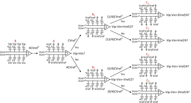
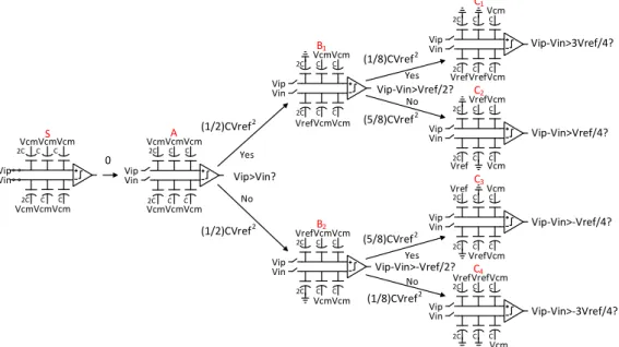
hence the conversion finished [2, 14]. Figure 3.4 shows all possible conversion steps for this ADC, including the switching energy per each step. The letters on top of every conversion step will be used in the next section to ease the reader’s job following the determination of the switching energy for each conversion step.
Switching Energy
The energy drawn from the reference voltage,Vref, to charge the top plate of a capacitor
C from its initial state, att = 0, to Vref, att =Tf, can be written according to Eq. 3.1,
3 . 3 . SA R A D C S S W I TC H I N G S C H E M E S CVref2 4CVref2 Vcm Vcm Vref Vcm Vcm
Vip Vip Vip Vip
4CVref2
S A
2C 4C C C
2C 4C C C
Vin Vin Vin Vin VrefVrefVref
2C 4C C C
2C 4C C C
Vip>Vin? Vref Vcm Vcm Vref Vref Vref 2C 4C C C
2C 4C C C
Vip-Vin>-Vref/4? C1 Vcm Vcm Vref Vref VrefVref 2C 4C C C
2C 4C C C
Vip-Vin>3Vref/4? Vref Vcm Vcm Vref Vref Vref 2C 4C C C
2C 4C C C
Vip-Vin>-3Vref/4? C4 C3 Vcm Vcm Vref Vref Vref Vref 2C 4C C C
2C 4C C C
Vip-Vin>Vref/4? C2 Vcm Vcm Vref VrefVref Vref B1 2C 4C C C
2C 4C C C
(1/4)CVref2 (13/4)CVref2 Vip-Vin>Vref/2? Vcm Vref Vref Vcm VrefVref B2 2C 4C C C
2C 4C C C
Vip-Vin>-Vref/2? Yes No Yes No Yes No (5/4)CVref2 (9/4)CVref2
Figure 3.4: Conventional 3 bit SAR ADC switching procedure.
E=
Z Tf
0
Vrefiref(t)dt (3.1)
Considering that iref(t) = −
dQ
dt and Q = CV, Eq. 3.1 can be rewritten as Eq. 3.2,
assuming that no more the current is drawn fromVref aftert= 1.
E=−Vref∆Q=−Vref (C∆V) (3.2) In order to derive the switching energy values exhibited in Figure 3.4, according to Eq. 3.2, the voltage difference between adjacent conversion steps must be calculated. To
do so, charge conservation equations will be used.
Sampling Phase,φS The sampling phase is the first step of a full conversion as shown
in Figure 3.4. In this case, the top plates are connected to the common-mode voltage and bottom plate sampling is used. Eq. 3.3 and Eq. 3.4 represent the charge at the top plates of both capacitor arrays during this phase.
Q+S= 4CVcm−Vip
+ 2CVcm−Vip
+CVcm−Vip
+CVcm−Vip
(3.3)
Q−
S= 4C(Vcm−Vin) + 2C(Vcm−Vin) +C(Vcm−Vin) +C(Vcm−Vin) (3.4)
Phase A,φA After the signal has been sampled in φS, the bottom plate of the MSB capacitor is switched toVref in the positive DAC and the other capacitors in this DAC
C H A P T E R 3 . A N A LYS I S O F SA R A D C S
the same time, the top plates are disconnected from Vcm. This operation will force the
DAC voltages to change since the charge is conserved. Eq. 3.5 and Eq. 3.6 represent the charge at the top plates of both capacitor arrays during this phase.
Q+A= 4CVDAC+
A
−Vref+ 2CV+
DACA
−0+CV+
DACA
−0+CV+
DACA
−0 (3.5)
Q−
A= 4C
V−
DACA−0
+ 2CV−
DACA−Vref
+CV−
DACA−Vref
+CV−
DACA−Vref
(3.6) Since the charge is conserved, by equatingQS toQA, the output voltages of the DACs,
VDAC, are calculated in Eq. 3.7 and Eq. 3.8.
Q+S=QA+⇔V+
DACA=Vcm
−Vip+Vref
2 (3.7)
Q−
S=Q
−
A⇔V
−
DACA=Vcm−Vin+
Vref
2 (3.8)
The resulting voltages are evaluated by the comparator, according to Eq. 3.9.
∆V
DAC >0⇔VDAC+ A
−V−
DACA>0 (3.9)
The energy drawn from Vref, in the transition from φS to φA, can be calculated according to Eq. 3.2. Expanding Eq. 3.2 to the present case results in Eq. 3.10 and Eq. 3.11.
EA+=−Vref 4C
VDAC+
A
−Vref−Vcm−Vip
!
= 2CVref2 (3.10)
E−
A=−Vref 2C V− DACA
−Vref−(Vcm−Vin)
+C
V−
DACA
−Vref−(Vcm−Vin)
+C
V−
DACA−Vref
−(Vcm−Vin)
= 2CVref2
(3.11)
Therefore, the total DAC energy from the sampling phase to the present phase is given by Eq. 3.12.
EA=E+A+E
−
A= 4CV 2
ref (3.12)
Phase B,φB Depending on the comparator’s decision from Eq. 3.9, the MSB capacitor
on the positive side of the DAC remains connected toVref, leading to phase B1,φB1, or
is switched tognd, generating phase B2,φB2. In any of the cases, the MSB-1 capacitor is connected toVref. The complementary operation is performed on the negative side of the
DAC.
3 . 3 . SA R A D C S S W I TC H I N G S C H E M E S
Phase B1,φB1 Due to the switching action in the bottom plates of the DAC, the
top plate voltages are changed, in order to keep the total charge constant. Eq. 3.13 and Eq. 3.14 represent the charge at the top plates of both capacitor arrays duringφB1.
QB+ 1= 4C
VDAC+
B1−Vref
+ 2C
VDAC+
B1−Vref
+C
VDAC+
B1−0
+C
VDAC+
B1−0
(3.13)
Q−
B1= 4C
V−
DACB1 −0
+ 2C
V−
DACB1 −0
+C
V−
DACB1 −Vref
+C
V−
DACB1 −Vref
(3.14) Due to the charge conservation, the resulting top plate voltages are expressed in Eq. 3.15 and Eq. 3.16. These voltages are evaluated by the comparator similarly to Eq. 3.9, however considering the voltages now present in the DACs.
Q+S=QB+1⇔V+
DACB1 =Vcm
−Vip+3
4Vref (3.15)
Q−
S=Q
−
B1⇔V −
DACB1 =Vcm
−Vin+ Vref
4 (3.16)
The energy drawn from Vref, in the transition from φA to φB1, can be calculated
according to Eq. 3.2. Expanding Eq. 3.2 to the present case results in Eq. 3.17 and Eq. 3.18.
EB+
1=−Vref
4C "
VDAC+
B1−Vref
−V+
DACA−Vref #
+ 2C
"
VDAC+
B1 −Vref
−V+
DACA −0 # =1 2CV 2 ref (3.17) E−
B1=−Vref
C " V−
DACB1−Vref
−V−
DACA−Vref #
+C
"
V−
DACB1 −Vref
−V−
DACA
−Vref
# =1 2CV 2 ref (3.18)
Therefore, the total DAC energy from the previous phase to the present phase is given by Eq. 3.19.
EB1=E
+ B1+E
−
B1=CV
2
ref (3.19)
Phase B2,φB2 The methodology to determine the DAC switching energy to phase
B2 is similar to that used to calculate the switching energy to phase B1. Thus, Eq. 3.20 and Eq. 3.21 represent the charge at the top plates of both capacitor arrays during this phase.
Q+B 2= 4C
VDAC+
B2−0
+ 2C
VDAC+
B2−Vref
+C
VDAC+
B2−0
+C
VDAC+
B2−0
C H A P T E R 3 . A N A LYS I S O F SA R A D C S
Q−
B2= 4C
V−
DACB2 −Vref
+ 2C
V−
DACB2 −0
+C
V−
DACB2 −Vref
+C
V−
DACB2 −Vref
(3.21) Once the DACs are settled, the voltages at the top plates are derived using charge conservation equations Eq. 3.22 and Eq. 3.23.
QS+=Q+B2⇔V+
DACB2 =Vcm
−Vip+1
4Vref (3.22)
Q−
S =Q
−
B2⇔V −
DACB2=Vcm
−Vin+3
4Vref (3.23)
The energy required to produce this voltage changes is calculated in Eq. 3.24 and Eq. 3.25. Eq. 3.26 determines the total energy required by the DAC.
EB+
2=−Vref
2C "
VDAC+
B2−Vref
−V+
DACA−0 # =5 2CV 2 ref (3.24) E−
B2=−Vref
4C " V−
DACB2−Vref
−V−
DACA−0 #
+C
"
V−
DACB2−Vref
−V−
DACA−Vref #
+C
"
V−
DACB2 −Vref
−V−
DACA
−Vref
# =5 2CV 2 ref (3.25)
EB2=EB+ 2+E
−
B2= 5CV
2
ref (3.26)
Phase C,φC The LSB is determined in the last phase of the conversion, which corre-sponds to phaseCin the 3 bit conventional SAR ADC depicted in Figure 3.4. Again, the conversion path depends on the previous decision of the comparator, i.e. the comparator’s decision from phase B.
Phase C1,φC1 This phase is reached if the successive approximation algorithm has
not taken wrong steps through the full conversion. As previously explained, the charge at the top plates during this phase can be expressed by Eq. 3.27 and Eq. 3.28.
QC+ 1= 4C
VDAC+
C1 −Vref
+ 2C
VDAC+
C1 −Vref
+C
VDAC+
C1 −Vref
+C
VDAC+
C1 −0
(3.27)
Q−
C1= 4C
V−
DACC1 −0
+ 2C
V−
DACC1 −0
+C
V−
DACC1 −0
+C
V−
DACC1 −Vref
(3.28) The charge conservation principle allow us to calculate the DACs top voltages accord-ing to Eq. 3.29 and Eq. 3.30.
Q+S=QC+ 1⇔V
+
DACC1 =Vcm
−Vip+7
8Vref (3.29)
3 . 3 . SA R A D C S S W I TC H I N G S C H E M E S
Q−
S=Q
−
C1 ⇔V−
DACC1 =Vcm
−Vin+1
8Vref (3.30)
The energy consumed in the switching action of each DAC is determined in Eq. 3.31 and Eq. 3.32. The energy consumed by both arrays is given in Eq. 3.33.
EC+
1=−Vref
4C "
VDAC+
C1−Vref
−
VDAC+
B1−Vref # + 2C
VDAC+
C1 −Vref
− V+
DACDACB
1 −Vref
! + C
VDAC+
C1−Vref
− V+
DACDACB 1 −0 ! = 1 8CV 2 ref (3.31) E−
C1=−Vref
C " V−
DACC1 −Vref
−
V−
DACB1 −Vref
# =1 8CV 2 ref (3.32)
EC1=EC+ 1+E
−
C1=
1 4CV
2
ref (3.33)
Phase C2,φC2 If the comparator’s decision in phaseφB1is contrary, the next step in
successive approximation algorithm isφC2. Eq. 3.34 and Eq. 3.35 express the top plate
charge for each DAC array.
Q+C2= 4C
VDAC+
C2 −Vref
+ 2C
VDAC+
C2 −0
+C
VDAC+
C2 −Vref
+C
VDAC+
C2 −0
(3.34)
Q−
C2= 4C
V−
DACC2 −0
+ 2C
V−
DACC2 −Vref
+C
V−
DACC2 −0
+C
V−
DACC2 −Vref
(3.35) The DACs top voltages can be determined according to Eq. 3.36 and Eq. 3.37.
Q+S=Q+C 2⇔V
+
DACC2=Vcm
−Vip+5
8Vref (3.36)
Q−
S=Q
−
C2 ⇔V−
DACC2 =Vcm
−Vin+3
8Vref (3.37)
The energy drawn fromVref, in the transition fromφB1toφC2, is computed in Eq. 3.38
and Eq. 3.39.
EC+ 2=
−Vref
4C "
VDAC+
C2 −Vref
−
VDAC+
B1 −Vref
#
+
2C
"
VDAC+
C2−0
−
VDAC+
B1−Vref #
+C
"
VDAC+
C2−Vref
−
VDAC+
C H A P T E R 3 . A N A LYS I S O F SA R A D C S
E−
C2=−Vref
2C " V−
DACC2−Vref
−
V−
DACB1−0 #
+
C
"
V−
DACC2 −Vref
−
V−
DACB1 −Vref
# =13 8 CV 2 ref (3.39)
Therefore, the total DAC energy fromφB1toφC2is given by Eq. 3.40.
EC2=E
+ C2+E
−
C2=
13 4 CV
2
ref (3.40)
Phase C3,φC3 FromφB2 toφC3, the bottom plate voltage of the 2 MSB capacitors is
modified. Therefore, the top plate voltage of the capacitor arrays changes in order to keep the total charge constant. Eq. 3.41 and Eq. 3.42 represent the charge at the top plates of both capacitive DACs during this phase.
Q+C 3= 4C
VDAC+
C3
−0+ 2C
VDAC+
C3 −Vref
+C
VDAC+
C3 −Vref
+C
VDAC+
C3 −0
(3.41)
Q−
C3= 4C
V−
DACC3−Vref
+ 2C
V−
DACC3−0
+C
V−
DACC3−0
+C
V−
DACC3−Vref
(3.42) The resulting top plate voltages, due to the charge conservation, are expressed in Eq. 3.43 and Eq. 3.44.
Q+S=QC+ 3⇔V
+
DACC3 =Vcm
−Vip+3
8Vref (3.43)
Q−
S=Q
−
C3⇔V −
DACC1 =Vcm
−Vin+5
8Vref (3.44)
The energy required to produce this voltages is expressed in Eq. 3.45 and Eq. 3.46. Eq. 3.47 determines the total energy required by the DAC.
EC+
3=−Vref
2C "
VDAC+
C3 −Vref
−
VDAC+
B2 −0 # + C "
VDAC+
C3 −Vref
−
VDAC+
B2 −0 # =5 8CV 2 ref (3.45) E−
C3= −Vref
4C " V−
DACC3 −Vref
−
V−
DACB2 −Vref
#
+
C
"
V−
DACC3 −Vref
−
V−
DACB2 −Vref
# =5 8CV 2 ref (3.46)
EC3=EC+ 3+E
−
C3=
5 4CV
2
ref (3.47)
3 . 3 . SA R A D C S S W I TC H I N G S C H E M E S
Phase C4,φC4 The last phase depicted in Figure 3.4 isφC4, which corresponds to all
conversion steps taken in the wrong direction. Similarly to what was done before, the top plate charge for each array is expressed by Eq. 3.48 and Eq. 3.49.
QC+4= 4CVDAC+
C4−0
+ 2C
VDAC+
C4 −0
+C
VDAC+
C4 −Vref
+C
VDAC+
C4 −0
(3.48)
Q−
C4= 4C
V−
DACC4
−Vref+ 2C
V−
DACC4 −Vref
+C
V−
DACC4 −0
+C
V−
DACC4 −Vref
(3.49) The voltages at the DACs top plates are derived using the charge conservation princi-ple in Eq. 3.50 and Eq. 3.51.
Q+S=Q+C 4
⇔V+
DACC4=Vcm
−Vip+1
8Vref (3.50)
Q−
S=Q
−
C4⇔V −
DACC4 =Vcm
−Vin+7
8Vref (3.51)
The energy drawn from Vref, in the transition from φB2 to φC4, is determined in
Eq. 3.52 and Eq. 3.53.
E+C
4=−Vref
C "
VDAC+
C4−Vref
−
VDAC+
B2 −0 # =9 8CV 2 ref (3.52) E−
C4= −Vref
4C " V−
DACC4 −Vref
−
V−
DACB2 −Vref
#
+
2C
"
V−
DACC4−Vref
−
V−
DACB2 −0
#
+C
"
V−
DACC4−Vref
−
V−
DACB2 −Vref
# = 9 8CV 2 ref (3.53) Hence, the total energy due to switching is obtained in Eq 3.54.
EC4=E
+ C4+E
−
C4=
9 4CV
2
ref (3.54)
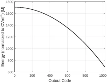
Final Remarks The conventional switching scheme is not very energy efficient,
C H A P T E R 3 . A N A LYS I S O F SA R A D C S
Output Code
0 200 400 600 800 1000
Energy (normalized to CVref
2 ) [fJ]
600 800 1000 1200 1400 1600 1800
Figure 3.5: 10 bit SAR ADC switching energy as a function of the output code - conven-tional switching scheme.
3.3.2 Merged Capacitor Switching (MCS) or Vcm-based Switching Scheme
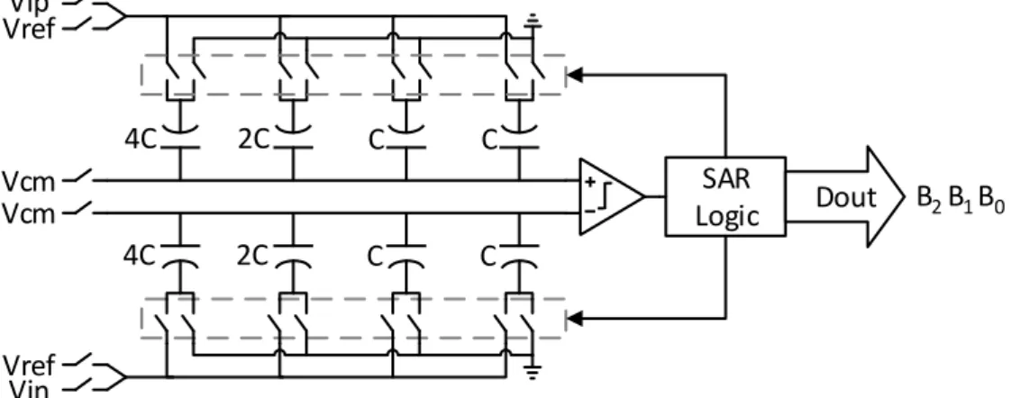
The Vcm-based switching scheme [16] does not follow the conventional successive ap-proximation algorithm. Instead, as the signal is sampled on the top plates, the switching action can be performed after the comparator’s decision, hence no wrong steps in the con-version are taken. Furthermore, since no switching is required in the first comparison, the MSB capacitor can be removed from the DAC arrays which halves the total capacitance of the DACs, Figure 3.6.
SAR Logic
Vcm Vref
2C C C
2C C C
Vin Vip
Dout B B B2 1 0 Vcm
Vref
Figure 3.6: 3 bit SAR ADC Vcm-based architecture - differential circuit schematic.
The conversion starts with the sampling phase,φS. As mentioned before, the input
signal is now sampled on the top plates of the DAC arrays, while the bottom plates are connected to the common mode voltage,Vcm. In the next phase,φA, the top plates are dis-connected from the inputs and the bottom plates remain dis-connected toVcm. Notice that as
3 . 4 . O T H E R SA R A R C H I T E C T U R E S
no energy is required in this transition. At this moment, the comparator takes its first decision. In caseVip> Vin, the bottom plate of the MSB-1 capacitor in the positive DAC is
switched tognd, whereas the MSB-1 capacitor in the other capacitive array is connected toVref. If the comparison’s result is contrary, the complementary operation is performed. Notice that all the other bottom plates remain connected toVcm and, regardless of the
comparator’s output, the capacitance switched is the same. After the DACs are settled, the comparator decides the MSB-1 bit,φB, and the process is repeated for the remaining bits, as depicted in Figure 3.7.
Vin Vip Vin Vip Vcm C 2C C VcmVcm 0 C 2C C VcmVcmVcm VcmVcmVcm VcmVcmVcm C 2C C C 2C C Vip>Vin? Yes No Vip-Vin>-Vref/2? Yes No Vin Vip C 2C C C 2C C VrefVrefVcm Vcm Vin Vip C 2C C C 2C C Vref Vcm VrefVcm Vin Vip C 2C C C 2C C VrefVcm Vref Vcm Vin Vip C 2C C C 2C C VrefVrefVcm Vcm Vin Vip C 2C C C 2C C VrefVcmVcm VcmVcm Vin Vip C 2C C C 2C C VcmVcm VrefVcmVcm Vip-Vin>Vref/2? Yes No (1/2)CVref2 (1/2)CVref2 (1/8)CVref2 (5/8)CVref2 (5/8)CVref2 (1/8)CVref2 S A B1 B2 C1 C2 C3 C4 Vip-Vin>-3Vref/4? Vip-Vin>-Vref/4? Vip-Vin>Vref/4? Vip-Vin>3Vref/4?
Figure 3.7: 3 bit SAR ADC Vcm-based switching procedure.
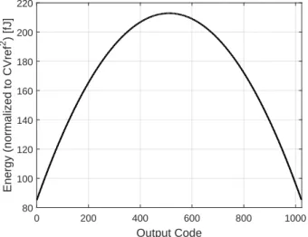
Besides showing all the possible conversion steps, Figure 3.7 also displays the DAC switching energy. The determination of these values is performed in a similar way to what was done to the conventional switching scheme, therefore it will not be repeated in this section. In Figure 3.8, the DAC switching energy is exhibited as a function of the output code for a SAR ADC using this switching scheme. Notice that the energy is completely symmetric as expected. Figure 3.8 also confirms that the Vcm-based switching method is much more energy efficient when compared to the conventional switching scheme.
3.4 Other SAR Architectures
Despite being used for moderate-speed, medium-resolution applications, SAR ADCs have found their way into other application spaces and are being used in several ways [25, 26].
High-speed SAR ADCs are being reported in recent scientific publications and con-ferences, making use ofTime-Interleavingtechniques [5, 26] andMultiple-bits per Cycle
architectures [8, 26]. In [27], a combination of these two techniques is used.
C H A P T E R 3 . A N A LYS I S O F SA R A D C S
Output Code
0 200 400 600 800 1000
Energy (normalized to CVref
2 ) [fJ]
80 100 120 140 160 180 200 220
Figure 3.8: 10 bit SAR ADC switching energy as a function of the output code - Vcm-based switching scheme.
In [1], a SAR ADC specially developed for biomedical application makes use of several comparators to create a bypass-window which allows to skip some conversion steps, hence its power consumption is decreased.
A SAR ADC coarse-fine converter in which the residual voltage after the successive approximation coarse conversion is converted to time domain and a TDC is used to solve the LSBs is presented in [31].
SAR ADCs relying on Charge Sharing techniques, rather than Charge Redistribu-tion, achieving very high energy-efficiency have recently been reported. However, these
architectures are only suitable for very low speed, small resolution applications [18].