Universidade do Minho
Escola de Engenharia
Pedro
Manuel
de
Lima
Gomes
Caldelas
Production and characterisation of
composites materials based on
Ge nanoparticles-doped dielectric layer
M in ho 2 00 9 Pe dr o M an ue l d e Li m a G om es C al de la sP ro d u ct io n a n d c h a ra ct e ri sa ti o n o f co m p o si te s m a te ri a ls b a se d o n G e n a n o p a rt ic le s-d o p e d d ie le ct ri c la ye r
Tese
de
Mestrado
Processamento
e
Caracterização
de
Materiais
Trabalho efectuado sob a orientação da
Professora Doutora Maria Jesus Matos Gomes
e
da
Professora Doutora Ana Maria Pires Pinto
Universidade do Minho
Escola de Engenharia
Pedro
Manuel
de
Lima
Gomes
Caldelas
Production and characterisation of
composites materials based on
É AUTORIZADA A REPRODUÇÃO PARCIAL DESTA TESE, APENAS PARA EFEITOS DE INVESTIGAÇÃO, MEDIANTE DECLARAÇÃO ESCRITA DO INTERESSADO, QUE A TAL SE COMPROMETE
Escola de Engenharia
Pedro Manuel de Lima Gomes Caldelas
Production and characterisation of
composites materials based on
Ge nanoparticles-doped dielectric layer
Tese de Mestrado
Processamento e Caracterização de Materiais
Trabalho efectuado sob a orientação da
Professora Doutora Maria Jesus Matos Gomes
e da
É AUTORIZADA A REPRODUÇÃO INTEGRAL DESTA TESE/TRABALHO APENAS PARA EFEITOS DE INVESTIGAÇÃO, MEDIANTE DECLARAÇÃO ESCRITA DO INTERESSADO, QUE A TAL SE COMPROMETE.
Universidade do Minho, / /
Acknowledgments
Acknowledgments
Many persons had, somehow, contributed to this work. First of all, I have to thank Prof.ª Maria de Jesus Gomes for the close supervision and Prof.ª Ana Pinto for all the help and guidance whenever required. Several other researchers colleagues and Professors working at the Physics Department of University of Minho also gave their contribute. I must not forget to thank Prof.ª Anabela Rolo for the all-fruitful discussions and help in performing the Raman measurements, as well as Dr. Adil Chahboun for the help in performing the photo-luminescence measurements and their results interpretation. Other people like Anatoly Khodorov, Carlos Batista, Sara Pinto, Sergey Levichev, and Prof. Mário Pereira must also be
mentioned.It was a true pleaser to have the opportunity of working, discussing and fraternize
with all of you.
Others, from outside the University of Minho, have also contributed to this work in performing several characterisation techniques not available at home. Their efforts are equality thankful and, because of that, their names are mentioned along the text when presenting each of the characterisation techniques on which they were involved.
Last but not least, I would like to address my special thanks to my wife Paula for all her support and understanding during all this time, and to dedicate this dissertation to my adorable baby daughter Sara, which has inspired me and gave me the strength to be able to complete it.
Abstract
Abstract
Production and characterisation of composites materials based on Ge nanoparticles-doped dielectric layer
The main goal of this project was the processing and structural, chemical and optical characterisation of nanocomposite thin film Germanium (Ge) semiconductor nanoparticles
(NPs) embedded in Alumina (Al2O3) layer. Such type of materials structures has several
potential applications, mainly in electronics and optoelectronic devices like it is the case of memory or light emitting devices (LED’s). Stand-alone Alumina films were initially produced and studied as the reference starting point.
The nanocomposite were produced by RF-magnetron sputtering technique. A significant number of characterisation techniques were used in order to evaluate the nanocomposite properties, namely X-ray diffraction (XRD), Raman scattering, scanning and transmission electron microscopy (SEM and TEM), Rutherford backscattering spectroscopy (RBS), and photoluminescence (PL).
The results and discussion, based on the particular findings revealed by the detailed analysis of all data from each characterisation technique, are presented cautiously. The study of the deposition and annealing parameters led to processing parameters optimization. The ability to (re)produce such type of materials structures is discussed. The conclusions are presented in a concise way. Ultimately, some light emission that might be related to excitonic recombination in the Germanium nanocrystals was observed during PL measurements. The temperature dependence of the PL demonstrates the confinement effect.
Resumo
Resumo
Produção e caracterização de materiais compósitos baseados em matriz dieléctrica dopada com nanopartículas de Ge
Este trabalho teve como objectivo o processamento e a caracterização estrutural, química e óptica de filmes finos de nanocompósitos de Alumina com nanopartículas de Germânio. Estes materiais possuem várias potenciais aplicações, sobretudo em dispositivos electrónicos e opto-electrónicos como são o caso de dispositivos de memória ou emissores de luz (vulgarmente denominados LED´s). Filmes de Alumina foram inicialmente estudados para servirem como ponto inicial de referência.
Os filmes de nanocompósitos foram produzidos por pulverização catódica em magnetrão por rádio frequência (RF-magnetron sputtering). A avaliação das propriedades dos filmes foi efectuada recorrendo a diversas técnicas de carcaterização, nomeadamente difracção de Raios-X (XRD), difusão Raman, espectroscopia electrónica de varrimento e de transmissão (SEM e TEM), espectroscopia de retrodispersão de Rutherford (RBS), e fotoluminescência (PL).
Os resultados e a discussão, baseados nas conclusões individuais reveladas pela análise detalhada de todos os dados provenientes de cada técnica de caracterização, são apresentados de forma prudente. Os parâmetros de deposição e recozimento para a produção dos materiais
nanocompósitosforam estudados e optimizados. A capacidade de (re)produzir tais estruturas
de materiais é discutida. As conclusões são apresentadas de forma concisa. No final, os resultados de PL revelaram uma emissão de luz que poderá estar associada à recombinação excitónica dos nanocristais de Germânio. A dependência da temperatura do PL demonstra o efeito de confinamento quântico.
Index
Index
Acknowledgments ... iii Abstract...v Resumo ... vii Index ...ixList of abbreviations and acronyms ...xi
List of symbols... xiii
List of figures...xv
Chapter 1 – Introduction ...1
1.1 Importance of the research area ...3
1.1.1 Semiconductor Nanocrystals, properties and applications ...3
1.1.2 Scope of the Thesis ...5
1.2 PVD versus CVD processes ...6
1.3 Sputtering...7
1.4 Magnetron sputtering...9
1.4.1 Balanced vs unbalanced magnetron fields...11
1.5 Annealing heat treatment ...12
Chapter 2 – Experimental procedures...15
2.1 Materials production ...17 2.1.1 Films growth ...17 2.1.2 Annealing...22 2.2 Materials characterisation ...25 2.2.1 X-ray diffraction ...25 2.2.2 Raman scattering...28 2.2.3 RBS...30 2.2.4 XPS ...31 2.2.5 SEM ...33
2.2.6 TEM, HRTEM, and SAD ...34
2.2.7 Optical absorption...36
Index
Chapter 3 – Results and discussion...41
3.1 X-ray diffraction elements identification...44
3.2 Al2O3 films...45
3.3 Ge doped Al2O3 films ...50
3.3.1 SEM analysis ...50
3.3.2 RBS and XPS chemical analysis ...52
3.3.3 XRD and Raman...59
3.3.4 TEM, HRTEM, and SAD ...70
3.3.5 Absorption ...73
3.3.6 Photoluminescence ...75
Chapter 4 – Conclusion...79
References ...83
Annex I – Properties of Alumina, Germanium and Silicon bulk materials ...87
Germanium (Ge), 100%...88
Silicon (Si), 100%...89
Alumina (Al2O3), 99.9%...90
Annex II – Table of the deposition parameters...93
Annex III – Table of the annealing parameters ...97
Annex IV – RBS spectra...101
Annex V – XPS survey spectra...105
List of abbreviations and acronyms
List of abbreviations and acronyms
A – Optical Absorbance or Optical density a-Ge – Amorphous Germanium
c-Ge – Crystalline Germanium DOS – Density of States FS – Fused Silica
GIXRD – Glancing-angle Incidence X-ray Diffraction
HRTEM – High Resolution Transmission Electron Microscopy MIS – Metal–Insulator–Semiconductor
NCs – Nanocrystals NPs – Nanoparticles PL – Photoluminescence
PLE – Photoluminescence Excitation QDs – Quantum Dots
R – Annealed (from the Portuguese word “Recozida”) RBS – Rutherford Backscattering Spectrometry RF – Radio Frequency
RT – Room Temperature
SAD – Selected Area Diffraction
sccm – standard cubic centimetres per minute SEM – Scanning Electron Microscopy TEM – Transmission Electron Microscopy XPS – X-ray Photoelectron Spectroscopy XRD – X-ray Diffraction
List of symbols
List of symbols
λ
– mean free pathΦ
– magnetic fluxFWHM
β
– full width at half maximum (FWHM) of the diffraction peakB – magnetic field d – thickness D – mean diameter
ε
– dielectric constant k – extinction coefficient n – refractive index p – pressure pAr – Argon pressure P – powerPRF – radio-frequency sputtering power
t – time
Tdep – deposition temperature
a
T – annealing temperature
List of figures
List of figures
Chapter 1
Fig.1.1 – Schematic showing the main procedural differences in films deposited by PVD or CVD: (a) conformity or uniformity, and (b) directionality.
Fig.1.2 – (a) Atomic interaction in the sputtering target, taken from [13]; (b) Basic schematic of the inside of a vacuum chamber showing the sputtering process.
Fig.1.3 – Draft of a generic rectangular planar magnetron showing (a) its quasi-rectangular sputter erosion track formed inside the magnetic field lines and (b) the cross section view taken through the plane B-B’ showing: 1-nonmagnetic metal case, 2-insulater, 3-magnetizable rear yoke, 4-permanent magnets, and 5-magnetizable pole pieces. In (b), the vacuum seals and the cooling water channels are omitted for simplicity. Adapted from [15].
Fig.1.4 – Cross section draft of the field pattern produced by (a) a rectangular planar magnetron with balanced field and (b) a circular planar magnetron with unbalanced field, both having a matched set of magnets. Reproduced from [15].
Fig.1.5 – Helical orbit executed by an electron leaving the target in the presence of a magnetic field B.
Chapter 2
Fig.2.1 – The Alcatel SCM650 apparatus at the Thin Films Laboratory.
Fig.2.2 – Overall block diagram of the vacuum pumping system associated to the Alcatel SCM650 apparatus. Adapted from [25].
Fig.2.3 – Simplified schematic of the inside view of the vacuum chamber. Adapted from [25].
Fig.2.4 – Schematic cross-section view of the magnetron structure showing the Al2O3 target and anode
plate properly mounted. (Note that relative dimensions are not in scale).
Fig.2.5 – Description of the three target configurations in terms of quantity and positioning of the Ge pieces placed on top of the alumina target.
Fig.2.6 – Schematic showing the placement of the samples-holder over the target (a) and criteria numbering established to label the samples of each series regarding their positioning on the holder. Fig.2.7 – Annealing system used: (a) oven, (b) thermocouple, (c) temperature controller, (d) quartz tube, (e) gas lines, (f) rotary pump, (g) diffusion pump and (h) pressure gauges.
Fig.2.8 – Experimental annealing ramp obtained for the 800ºC/1hour annealing processes.
Fig.2.9 – Schematic representation of an X-ray diffraction measurement made with Bragg-Brentano geometry.
Fig.2.10 – Schematic representation of the system used in the Raman scattering measurements (microanalysis set up in backscattering geometry).
List of figures
Fig.2.11 – (a) Schematic of a classic collision and backscattering of a lighter projectile of mass M1
with a heavier target particle of mass M2 initially at rest inside a target material (the recoil of the target
particle is not plotted); (b) Schematic of backscattering event from a thick elemental sample and a typical resulting spectrum.Adapted from [33].
Fig.2.12 – SEM image of a thin TEM sample milled by focused ion beam. The thin membrane is suitable for TEM examination; however, at approximatelly 300nm thick, it would not be suitable for High-Resolution TEM without further milling. Adapted from non-specified source.
Fig.2.13 – Representative schematic of the absorption measurements. Light of intensity I0 incident
upon a sample of thickness d undergoes a loss in intensity upon passing through the sample. The final intensity measured is I.
Fig.2.14 – Schematic of the PL experimental setup.
Chapter 3
Fig.3.1 – X-ray diffraction spectra of two different samples of Al2O3 films obtained with
Brag-Brentano geometry: a) sample AC22Si, deposited at 500ºC using 50W RF-power for 5,5 hours under an Argon pressure of 4.0×10⁻³mbar; b) sample AE22Si, deposited at 500ºC using 80W RF-power for 3 hours under an Argon pressure value of 2.0×10⁻³mbar.
Fig.3.2 – Comparison of the GIXRD spectra of the annealed samples AC22SiR3 and AE22SiR3. Spectrum obtained from sample AC21Si is shown at the inset. All three spectra obtained at the ESRF. Fig.3.3 – a) transmission spectra of three different Al2O3 films deposited at 500ºC over glass
substrates, presenting very high transparency across all wavelength UV-visible-NIR; b) XRD spectrum from two as-grown Al2O3 films deposited at 500ºC over Fused Silica substrates, revealing
their amorphous nature. (Deposition parameters PRF, pAr and t shown between parentheses).
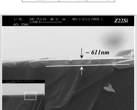
Fig.3.4 – Picture of a typical Alumina film (sample AC3.1) deposited on glass. Although it is a quite transparent sample, the contour of the film is still visible. For comparison, the inset picture shows the look of a piece of a sample from the same series deposited on Silicon substrate (sample AC21Si). Fig.3.5 – Cross-section SEM picture obtained for sample Z22Si: estimated thickness of 611nm. Fig.3.6 – Top view surface picture of sample Z21Si, obtained by SEM. Darkest dots on the picture were not possible to identify. Some of themmay possibly be small areas with higher Ge concentration. Fig.3.7 – Typical fitting and simulation (inset) spectra obtained after RBS measuring of a Ge doped Al2O3 film (in the case, sample U22Si). Adapted from [38].
Fig.3.8 – In depth comparison of the Ge3d Oxide and Ge3d (inset) atomic percentages that were obtained for all three samples analysed by XPS.
Fig.3.9 – a) X-Ray diffraction spectra and b) Raman spectra from as-deposited Ge doped Al2O3 films,
grown on FS substrates with PRF = 50W and three different Argon pressures. GIXRD spectrum from
one of the samples (obtained with 1º theta incidence) is shown in the inset for comparison with the conventional XRD. The peaks marked with the symbol “+” are attributed to possible presence of very small alumina NCs. Adapted from [38].
List of figures
Fig.3.10 – X-ray diffractograms corresponding to the study of the different RF-sputtering power values that were tested. All samples corresponding to films deposited on Silicon(111) substrates, under the same Argon pressure (4.0×10⁻³mbar) and substrate temperature (500ºC) deposition parameters. Fig.3.11 – X-ray diffractograms (a)) and Raman spectra (b)) from as-deposited Ge/Al2O3 films grown
on Si(111) substrates using pAr = 4×10⁻³mbar; Comparison between the central samples from series T
and U. Adapted from [38].
Fig.3.12 – X-ray diffractograms of the central samples from the only two series (U and Z) that showed the presence of Ge NCs in the as-deposited Ge/Al2O3 films on Si(111) substrates.
Fig.3.13 – GIXRD spectrum of sample V21SiR2N2, annealed under Nitrogen atmosphere, where a
mixture of gamma and delta alumina phases seems to be favoured. Spectrum from the alumina sample AC22SiR3 is shown for comparison.
Fig.3.14 – GIXRD spectra of V22Si vs V22SiR, clearly reveals the annealing effect on the c-Ge when using an (low pressure) air atmosphere.
Fig.3.15 – XRD spectra of sample X23SiRAr vs X32Si, shown as the as-deposited reference sample. Figure clearly reveals the results of the annealing on the films crystallographic structure, namely the formation of c-Ge phase.
Fig.3.16 – XRD spectra of samples U21Si and V22Si, were no reflection peaks were found for the annealing performed under Argon atmosphere. Spectrum from sample V22SiRAr revealed no peaks besides the ones expected from the Silicon substrate, and the peaks on the spectrum of sample U21SiRAr are most probably a result of some Alumina grains.
Fig.3.17 – XRD spectra of the central samples from series BD and BN as a function of the annealing temperatures of 800ºC (R) and 900ºC (R2). The increase of the average NCs size can be related to the increase of the annealing temperature.
Fig.3.18 – X-ray difractograms (a) and Raman spectra (b) of the as-deposited (U12Si) and annealed (U12SiR) sample grown on a Si(111) substrate. Annealing was performed during one hour at 800ºC on a low air pressure atmosphere.Adapted from [38].
Fig.3.19 – Comparison between XRD spectra of as-grown vs. annealed U22Si sample. The Ge NCs mean diameter, estimated based on these spectra, showed a clear increasing improvement of the Ge Crystalline phase (D (U22Si) = 2.5nm; D (U22SiR) = 6.9nm).
Fig.3.20 - GIXRD spectrum of the annealed sample O12SiR. Ge NCs with an average size of approximately 4.8nm could be estimated after Lorentzian fitting of all five Ge reflection planes. Fitting of the (311) reflection peak is shown as an example. If considering only this peak the estimated size would by 5.1nm.
Fig.3.21 - GIXRD spectrum of the annealed sample Z22SiR. Average estimated Ge NCs size of 5.5nm could be estimated, after Lorentzian fitting all the five reflection peaks.
Fig.3.22 - TEM images from U22SiR (a) and Z22SiR (b). HRTEM images of film U22SiR (c) and (d) (data provided by U. Oslo).
Fig.3.23 - Histograms of the NC sizes found in samples U22SiR (a) and Z22SiR (b) (data provided by U. Oslo).
List of figures
Fig.3.24 – Selected area diffraction from sample Z22SiR. The brighter spots are from the Si substrate while the rings are from the many different orientations of the Ge crystals. The rings labeled ‘ring 1’ and ‘ring 2’ are unidentified but could originate from an Al2O3 phase.
Fig.3.25 – EDS analysis of samples U22SR and Z22SiR.
Fig.3.26 – Typical Absorption/Transmission spectra for samples deposited on a) Silicon or b) glass substrates.
Fig.3.27 – Spectral dependences of a) the refractive index (n) and b) the extinction coefficient (k) of the Ge QDs.
Fig.3.28 – Reference PL spectrum for the Si(111) substrates. A line with the Silicon band gap value at 1.107eV is shown as reference. Peak is not symmetrical, so it is shown fitted by two Gaussians. Fig.3.29 –A typical PL spectrum from Ge NCs/Al2O3 system, obtained at 10K for sample U22SiR.
Adapted from [10].
Fig.3.30 –Evolution of the peak P1 with temperature (squares), compared with the red shift of the Ge bulk band gap (Eg), calculated with Varshni relationship (continuous line). Adapted from [10].
Fig.3.31 –Temperature dependence of the peak P1 in between 10 to 300K. The dashed line is guide for eyes. Adapted from [10].
Chapter 1
Introduction
Introduction
1. Introduction
1.1 Importance of the research area
1.1.1 Semiconductor Nanocrystals, properties and applications
Semiconductor nanocrystals (NCs), sometimes also called quantum dots (QDs), are very small crystalline semiconductor material which contain tens or a few hundred atoms with sizes of a few nanometres. The term nanoparticles (NPs) is also frequently used when referring to materials at the nanometre scale. The first realization of QDs was linked to the inclusion of nano-size Cadmium Selenide (CdSe) and Cadmium Sulphide (CdS)
semiconductors in glasses [1]. Such red or yellow coloured glasses have been commercially
available as colour filters for decades. In 1985 Ekimov et al. [2] experimentally proved and theoretically modelled that these changes in colour were linked to the density of states (DOS)
determined by the size of the crystalline material.Below a certain size, the properties of the
crystalline material start to deviate significantly from bulk properties and strongly dependent on size. Finite size of the micro crystallites confines the motion of the quasiparticles (electron, hole and exciton) within its physical boundary. This is called quantum confinement. Quantum confinement modifies the DOS, which in turn leads to discretisation as well as enlarged spacing between the energy levels of electron and hole states. Thus one can observe an increase in the band gap as the optical absorption onset occurs at higher energies
(blue-shift) in the case NCs.
Since a long period of time, most research effort concentrates on QDs made of III-V compound semiconductors having direct band gap. Due to the indirect optical transition properties of group IV materials, less interest has been paid on bulk Silicon (Si) or Germanium (Ge) semiconductor materials in that their light emission efficiency is not good enough for optoelectronic applications [3]. However, visible photoluminescence (PL) from Si quantum structures is reported in several works. Yet, bulk Ge has a larger dielectric constant and smaller carrier masses compared to bulk Si, leading to a larger Bohr radius (24.3nm) than
that of bulk Si. Moreover, in Ge, the direct gap (E0 ~ 0.88eV) is close to the direct gap (Eg ~
0.75eV). Then, it is considered that quantum confinement effects would appear more pronounced in Ge than in Si, and Ge NCs would exhibit a direct-gap semiconductor nature
Introduction
[4]. Therefore, Ge NCs would be easier to change in terms of electronic structure around the band gap, making them attractive for potential applications after all [3]. In fact, it was suggested that when the size of an indirect gap semiconductor is reduced to few nanometers, the NC starts to resemble to a direct gap material. Thus electrons and holes can be independently confined into the infinite spherical potential [5]. The lowest energy of the
electron-hole pair E1 could be obtained, as a first approximation, by Kayanuma model [6]:
E1= Eg + (
π
2 ⋅ h2 2 ⋅µ
⋅ R2) −1.786 e2κ
R− 0.248 ERy * , (1.1)where Eg is the optical band gap of bulk crystalline Ge,
µ
is the reduced mass, ħ is thereduced Planck constant, and E*Ry the effective Rydberg energy. In this model, the
nanocrystals are assumed to be spherical with sphere radius R and dielectric constant k.
Nowadays, and during the last two decades or so, huge scientific interests and progresses in understanding these NCs contributed to the new branch of science known as Nanoscience. In short words, as a result of the quantum confinement effects the emission colour of semiconductor NCs can be dramatically modified by simply changing their size [7]. This fact is the main reason why they have been studied as having high potential for possible applications over different fields of science: ultra sensitive, multicolour and multiplexing applications in molecular biotechnology and bioengineering; device fabrication like lasers, large area photovoltaic thin-films or light-emitting devices (LEDs); quantum optical applications including quantum cryptography and quantum computation; optoelectronic and signal processing; etc… . Among devices for optoelectronic and nano-electronic, the use of
Metal–Insulator–Semiconductor (MIS)1 structures using Si and Ge semiconductor NCs have
also been reported to show good memory effects and low power operation at room temperature [8]. In fact, one of the most common structures used for memory or LED
purposes is the metal or poly-Si/SiOx/Si structure with Si NCs embedded in the SiOx layer.
However, alumina2 or stacked dielectrics are also used as dielectric matrix, and Ge and SiGe
nanocrystals are also often formed inside those matrices [9] and [10]. Still, in most of the
works found on the literature the nanocrystals have been grown inside a SiO2 matrix.
It is clear, however, that for different applications, NCs are to be embedded in different matrices. Exploiting their potential applications, it is necessary to have a better understanding
1 More commonly mentioned term is Metal-Oxide-Semiconductor (MOS), which are a type of MIS structures. 2 Alumina, the commercial term used when referring to Aluminium Oxide (AlO).
Introduction
on how the properties of the NCs are influenced by different environments. Some results
showed that MOS capacitors with Al2O3 dielectric exhibit sensitivity greater than that
obtained from MOS capacitors with SiO2. This higher sensitivity is attributed to higher
trapping efficiency in the Al2O3.
Constant shrinking of the thickness of gate dielectrics to below 2-3 nm has also led to a
search for alternative materials, whose dielectric constant is higher than that of SiO2, but
whose other properties remain similar to SiO2. Because of its similar band gap (9eV) and
more than twice as high dielectric constant (
ε
Al2O3=9 andε
SiO2 =3.9), Al2O3 is a good candidateto replace SiO2 as a gate dielectric material and is starting to be used in today’s modern
electronic technology. At the same time Al2O3 presents good mechanical properties, which
leads it to be, at least in theory, an ideal material for Si processing conditions [11] and [10]. After deposition, the final step of the production of such kind of structures containing NCs consists of an annealing process. This is, perhaps, the more effective way to change and control the size of the semiconductors NCs embedded in their dielectric matrices.
1.1.2 Scope of the Thesis
The first objective of the research work that has led to this thesis was to be able to produce composite films based on Ge nanoparticles-doped dielectric layer. The full characterisation of those produced structures and the results interpretation, both from the structural and the optical properties points of view, was the second goal of this work. Being mostly a practical work, no focus is given herein to theoretical formulations related with confinement regimes or density of states, for instance. Conclusions reflect almost exclusively the characterisation results and observations, rather than hypothesis formulation based on semiconductor theory.
By the end of the dissertation, the interpretation study of all the results and experiments that were carried out will, hopefully, be a useful reference contributing to further works in this field of knowledge.
Introduction
1.2 PVD versus CVD processes
Thin films can be produced using a panoply of different techniques based on PVD (Physical Vapour Deposition) or CVD (Chemical Vapour Deposition) processes. In a very simple way, one can distinguish PVD from CVD by saying that PVD processes consist on a material release (either by vaporisation or sputtering) from a source (target) and its transference into a certain surface (substrate) to form what is called a thin film, while in CVD processes the film formation involves a chemical reaction that takes place inside a reactor to which one or more gases must be supplied.
There are several different techniques based on both processes (Table 1.1) that can be more or less complex and expensive, and more or less effective, in producing thin films for a certain type of application.
Table 1.1 – Some techniques based on PVD and CVD processes.
PVD CVD
− DC-Glow Discharge Sputtering
− Evaporation (resistance, induction, e-beam) − Ion implantation
− MBE – Molecular Beam Epitaxy − PLD – Pulsed Laser Deposition − RF Sputtering
− High Density Plasma CVD − Hot-wire CVD
− LPCVD – Low Pressure CVD − MOCVD – Metal Organic CVD − PECVD – Plasma Enhanced CVD
Choosing the most efficient technique to reach a certain goal can be a difficult task. Nevertheless, there are some consensual general differences that we can say for sure about films produced either by PVD or CVD processes. Among those differences, two of the more relevant ones are related to conformity and directionality as shown in Fig.1.1. In PVD, the film deposition is a highly directional process mainly perpendicular to the target. If the surface of the part that is to be covered is very far from being parallel to the target, and/or if that part has some kind of cavities or holes, most probably the process will not be very efficient. However, PVD is a very effective process if the substrate is flat and placed parallel to the target. A chemical vapour deposition is a much more multidirectional and conformal process than a PVD one. So, thickness homogeneity on irregular shape or non-parallel to the target substrates can be achieved in a much more effective way using CVD. Another
Introduction
risks and costs than PVD techniques due to the necessary use of the gaseous materials. Some of these gases can be very dangerous to health. This is, of course, a big disadvantage of CVD when compared to PVD techniques.
PVD CVD
(a)
Conformal deposition
(b)
Highly directional deposition Multidirectional deposition
Fig.1.1 – Schematic showing the main procedural differences in films deposited by PVD or CVD: (a) conformity or uniformity, and (b) directionality.
1.3 Sputtering
Sputtering process is well known and one of the most commonly used methods for the deposition of thin films. It is widely used in the automotive, photovoltaic, recording and semiconductor industries. High melting point materials like ceramics and refractory metals, which are difficult to deposit by evaporation, are easily deposited using sputtering. Sputtering techniques range from a simple dc glow discharge sputtering which is limited to the sputtering of conductive targets, to RF sputtering where any target regardless of its conductivity can be
sputtered, and to a more sophisticated ion beam sputtering (IBS) in which very wellcontrolled
deposition of material is possible [12].
The verb to sputter originates from Latin sputare (to emit saliva with noise). The phenomenon was first described about 150 years ago by Grove (1852) and Plücker (1858), who reported vaporization and film formation of metal films by sputtering . Sputtering usually
Introduction
takes place at low pressure inside a vacuum chamber when the target (and cathode, a solid material plate) is “bombard” by atoms or ions that collide with it at a certain velocity (kinetic energy). These collisions and momentum transfer from the incoming particles cause the ejection of atoms and secondary electrons (Fig.1.2 (a)), starting a continuous erosion process in the superficial area of the target. In this area it is possible to observe a glow discharge, or plasma, which is a fluid of positive ions and electrons in a quasi-neutral electrical state [13].
In spite of being a highly directional process, all the atoms and secondary electrons released from the target in the sputtering process fly away from it in every direction and with different energies. The sputtered atoms (or atom clusters) that are “extracted” with enough kinetic energy will be deposited on the substrate placed in front of the target (Fig.1.2 (b)). The secondary electrons are accelerated and could originate new gas ions by colliding with new gas atoms, making possible the sustainability of the sputtering process. As we will see further on, a magnetron can increase the efficiency of this process.
Fig.1.2 – (a) Atomic interaction in the sputtering target, taken from [13]; (b) Basic schematic of the inside of a vacuum chamber showing the sputtering process.
The number of target atoms being deposited on the substrate per unit of time is associated
with the deposition rate value of the film, usually expressed in nm.min-1. Considering the
kinetic theory of gases, and knowing the values of the pressure ( p ) and temperature (T ) of
the sputtering gas inside the volume (v) of the chamber, it is possible to determine the
number of particles per unit of volume (nv) inside the chamber. This allows us to calculate
Atom, ion (a) Atom or ion with kinetic energy (b) Sputtering gas
Substrate and film growth
Atom ion Pumping Target (cathode) Power Supply
Introduction
the average distance between collisions for a gas molecule, known as mean free path (λ), by
using the simple expression
(
λ = 2nvσ)
−1, whereσ
is the effective cross sectional area forcollision that is equal to
π
d2, being d the molecule diameter [14].So, as we saw, at least one type of sputtering gas (usually inert and with heavy atoms, like Argon or Xenon) must be introduced inside the chamber in order that the sputtering process
can be started. Part of the atoms of the gas being used, let say Argon, becomes ionized (Ar+)
by exchanging electrons with its surroundings, usually after a short thermo electronic discharge inside the chamber. If other not inert gas like oxygen is used, the process is called “reactive sputtering”. Atoms of these gases will react with all the surfaces inside the chamber including, and most important, the film material(s) that are being deposited on the substrate surface. Some compounds different from the target(s) material(s) can be obtained in this way.
In the traditional sputtering process, a negative dc current is usually applied to the target(s) being used, which must be a conductor material. However, if the material we want to sputter is not a good conductor, it could not be used as an electrode because, in this case, positive charges will start accumulating on top of the target. After some time, the accumulation of charges would prevent the sputtering process to continue, since the gas ions inside the chamber will be repulsed from the target instead of being attracted to it. Changing the dc power supply by an ac power supply, able to deliver an alternating current polarisation to the target, can solve this problem. The frequency of this current is typically in the range of 5 to 30 MHz (radio-frequency, RF ), being 13.56MHz one of the most used nowadays. During the negative cycle of the alternating polarisation of the target ions are attracted to the cathode (target) and sputtering occurs, while in the positive cycle only the electrons are attracted to the target and the electrical potential equilibrium is maintained, since the possible positive charge accumulation during the negative cycle can now be cancelled.
1.4 Magnetron sputtering
The magnetron sputtering is a more recent and clever way to increase the efficiency of the sputtering process by placing the target onto a magnetron with the appropriate geometry. We can describe a magnetron as a solid metallic structure in which a certain number of permanent magnets are placed and distributed in such a way that a magnetic field can be created around
Introduction
them. The purpose of using a magnetic field is to make more efficient use of the electrons and cause them to produce more ionisation.
Based on reference [15], the first magnetron discharge device employing cylindrical-hollow cathodes with in-turned end flanges appeared in a 1936 article by F. M. Penning. The use of end flanges was a crucial development because it made possible the electrostatic containment of the plasma. At that time, when fitting his volt-ampere curve to an equation of
the type I ∝Vn, a voltage index n of 6.5 was obtained. A few years later, and also based on
reference [15], Penning and Moubis were able to reduce this value to 6, after communicating the first magnetron glow discharge device employing a cylindrical-post cathode with out-turned end flanges in 1939. Depending on design details, typical present day magnetrons have a voltage index which lies in the range 5 to 10. In the late 1960s and early 1970s, approximately thirty years after Penning’s 1939 sputtering work, the surge in sputter magnetron development resulted in the recognition of three generic types of sputter magnetrons: conical magnetrons, cylindrical magnetrons and planar magnetrons [15]. Within each type there may be big variations of design. In particular, the planar magnetron designation includes devices in which the sputter erosion track is circular, square, rectangular, or oval (race-track like). Besides its shape, there may be a single erosion track or a nested series of tracks. At Fig.1.3 it is possible to see a draft of a simple planar magnetron (a) and its cross-section taken through the plane B-B’ (b), including the connections to a power supply and the typical positioning of the substrate over the sputter target. The white dotted line in (b) indicates the original cathode (target) surface while the solid contours indicate the profile, which develops after a long period of sputter erosion.
An assembly of permanent magnets putted together inside a case produces the magnetic field in a “magnetron”. The magnets arrangement, typically an outside ring of magnets and an inside central cylindrical magnet with inverted magnetization, are in such a way that the field lines emerge from, arch over, and re-enter the sputter target plate. The case is connected to ground potential and functions as the anode of the discharge. The plasma is mainly formed in the tunnel defined by the field line arches.
Introduction
Fig.1.3 – Draft of a generic rectangular planar magnetron showing (a) its quasi-rectangular sputter erosion track formed inside the magnetic field lines and (b) the cross section view taken through the plane B-B’ showing: 1-nonmagnetic metal case, 2-insulater, 3-magnetizable rear yoke, 4-permanent magnets, and 5-magnetizable pole pieces. In (b), the vacuum seals and the cooling water channels are omitted for simplicity. Adapted from [15].
1.4.1 Balanced vs unbalanced magnetron fields
In Fig.1.4 (a) the same field of Fig.1.3 (b) rotated through 90º is shown. All the field lines that emanate from the central “north pole” are collected by the outlying south poles. The
magnetic flux (
φ
) is zero on the plane of symmetry. This magnetron has a “balanced” field.Fig.1.4 – Cross section draft of the field pattern produced by (a) a rectangular planar magnetron with balanced field and (b) a circular planar magnetron with unbalanced field, both having a matched set of magnets. Reproduced from [15].
(a) Anode plate (b)
Magnet Assembly Case (anode)
Magnetic Field Lines Sputter Erosion Track Sputter Target (Cathode) (a) (b) Substrate holder
Introduction
Fig.1.4 (b) represents the field pattern produced by the same matched set of magnets but in the case when the system has rotational symmetry. It is possible to see that the differences between the two cases of Fig.1.4 are quite remarkable. The zero-flux contour has become almost circular, resulting in the creation of a saddle point (marked SP in Fig.1.4 (b)) located approximately at one-half the cathode diameter in front of the cathode. This magnetron has an “unbalanced” field.
In a system like the one of the Fig.1.4 (b), the behaviour of the plasma highly depends on the presence of the anode plate. Namely, it depends on the value of its inner diameter. If the anode plate is dimensioned and placed like shown on Fig.1.4 (b) the migration of plasma beyond the zero-flux line will be largely suppressed. However, if the anode plate presents a inner diameter value bigger than the diameter of the zero flux contour line then the moderate-to-low energy electrons escaping from the cathode magnetic trap will be able to execute helical orbits around field lines which guide them far downstream from the cathode [15]. Anyway, and providing it does not suffer any collision, an electron describing a circular motion around a magnetic field B (see Fig.1.5) is compelled to travel a much bigger distance before reaching the cathode surface again, enlarging the probability of ionisation of the sputtering gas and, in this way, increasing the efficiency of the sputtering process.
Fig.1.5 – Helical orbit executed by an electron leaving the target in the presence of a magnetic field B.
1.5 Annealing heat treatment
The production of most of the films included a post-deposition thermal treatment: the annealing treatment. This heat treatment annealing process is very common and applied in the nucleation and/or size increase of NCs or nanoparticles (NP’s), even if they are inside some kind of matrix. It is, probably, the most important and effective method to control the NCs size. Independently of the production technique, several authors report different post-deposition annealing conditions (atmosphere and temperature) in order to control the nucleation and/or growth of semiconductor NCs embedded in dielectric matrixes. Some used
Magnetic field line Electron path
Introduction
a rapid thermal annealing (RTA) system, others a more conventional furnace system. The differences between these two kinds of annealing systems mainly relays on the annealing time, which, in comparison with the conventional systems, can be very much reduced using an RTA system. In both cases, however, the main goal prevails: nucleation and/or growth of NCs. Nevertheless, it may be interesting to say that, based on experience, if not all the necessary cares are taken in order to eliminate high temperature gradient and/or if the adhesion between the film and the substrate is not as good as it should be, annealing on an RTA system can provoke the peeling of the film due to the stress induced by thermal shock.
Even if considering only Ge embedded both in silica (SiO2) or alumina (Al2O3) dielectric
materials, a lot of works can be found mentioning annealing as a crucial step for the NCs formation ([11], [16], [17]).
Germanium bulk material has a melting point of approximately 937ºC, a density of 5.32 g/cc, and a cubic structure (diamond like). Aluminium oxide, α-alumina, has a much higher melting point (around 2054ºC), a density of 3.96 g/cc, and a rhombohedral crystalline structure (Corundum). However, crystalline alumina presents five more different polymorphs (or crystalline phases). Besides the alpha (α) phase, also gamma (γ), kappa (k), theta (θ), delta (δ) and sigma (σ) phases exist, but it is α-alumina who has the best thermo-mechanical properties. More complete data sheets, including the physical, mechanical, electrical, thermal, and optical properties of alumina, germanium, and also silicon and silica materials are presented in Annex I.
The kind of substrate used to grow the films can some times limit the annealing
temperature (Ta). If a normal glass substrate is used, let say microscope slides for instance,
the usual annealing temperature will be limited to approximately 500-550ºC [11]. Above this value, the glass will start to soften. Annealing under temperatures in the range of 700 to 900ºC are the most reported as being suitable for the formation/grow of Ge NCs embedded in a dielectric film. This implies that films must be deposited over a substrate material that can stand higher temperatures, clearly above the Ge melting point. Not only because of this, but mostly due to technological reasons, silicon substrates are probably the most used ones to grow this kind of films (Si melting point=1412ºC). It was reported that Ge NCs embedded in sapphire melt at 955±15ºC [18], a value which is a little bit above the Ge melting point. The
annealing time (ta), which is the time during which the samples are kept at the Ta, is another
Introduction
from a few minutes to several hours. Different kind of atmospheres including Nitrogen (N2)
([19]), a mixture of Hydrogen and Argon (H2+Ar) ([20] and [21]), Argon ([16] and [22]), or
clean air, both at low ([23] and [24]) or atmospheric pressure [11] are also used in the annealing process of Ge embedded in dielectric matrix. The exact pressure value of the annealing atmospheres is usually not mentioned in the bibliography, although it seems more or less obvious, at least for me, that it must be also controlled as an important parameter. Independently of the kind of system, furnace, and related accessories available to perform the annealing (thermocouple, pumping equipment, gas lines, etc.), all these parameters (temperature, pressure, atmosphere, and annealing time) can influence a certain annealing result and should be controlled during the annealing process.
Chapter 2
Experimental procedures
Experimental procedures Materials production
2. Experimental procedures
2.1 Materials production
The production of the composite materials based on Ge nanoparticles-doped dielectric layer includes the films growth and the annealing processes. Both were done in LFF-Laboratório de Filmes Finos (Thin Films Laboratory), at the Physics Department of University of Minho in Braga.
2.1.1 Films growth
Films growth was based on PVD (Physical Vapour Deposition) processes. Samples were prepared by RF-magnetron co-sputtering technique on an Alcatel SCM650 apparatus. Co-sputtering is synonymous of more than one material being sputtered simultaneously, meaning that more than one material was used as targets at the same time, as described below. In short, the Alcatel apparatus shown in Fig.2.1 is composed of a chamber, a vacuum system, power supplies and controllers/matching boxes, and an automatic control system that allows the setting of parameters like temperature, deposition time, sample-holder positioning/rotation (including substrate to target distance), gas fluxes, etc.
Fig.2.1 – The Alcatel SCM650 apparatus at the Thin Films Laboratory.From the right to the left:
1. Main block with deposition chamber (1.1), load-lock or pre-vacuum chamber (1.2), pumping system (1.3) and matching boxes (1.4);
2. Control panels cabinet; 3. Power supplies cabinet.
1. 2. 3. 1.3 1.1 1.2 1.4 1.4 1.4
Experimental procedures Materials production
Fig.2.2 shows an overall block diagram of the vacuum pumping system and in Fig.2.3 a schematic of the inside of the vacuum chamber is shown.
Fig.2.2 – Overall block diagram of the vacuum pumping system associated to the Alcatel SCM650 apparatus. Adapted from [25].
Fig.2.3 – Simplified schematic of the inside view of the vacuum chamber. Adapted from [25]. Chamber Pre-chamber Turbo molecular Pump Rotary Pump Rotary Pump Pressure gauge (Penning) Pressure gauge (Pirani) Pressure gauge (Pirani) N2 Ar
Sample-holder on the top side of the chamber
Disposition of the four Magnetrons over the floor structure of the chamber
Experimental procedures Materials production
Two materials were simultaneously used as target to produce the composite materials:
alumina (Al2O3), for the dielectric matrix, and Germanium (Ge) for the semiconductor NCs
doping. An Al2O3 plate (purity of 99.99%, 50mm diameter) was initially glued on a brass
backing plate using silver vacuum glue. After the drying period, they were properly mounted on the magnetron structure like is possible to observe on Fig.2.4. Here, we can see the cross section view of all the elements associated to the target. The anode plate used had a hole with
40mm in diameter in its centre. So, in practice, the useful area of the Al2O3 plate used as
target was ∼12,57cm2.
Fig.2.4 – Schematic cross-section view of the magnetron structure showing the Al2O3 target and anode
plate properly mounted. (Note that relative dimensions are not in scale).
On top of the Al2O3 target, 1cm2 piece(s) of unpolished polycrystalline Ge sheet (purity of
99.999%) were also placed as target(s) to produce the co-sputtered films. The number of the
Ge pieces and their position over the Al2O3 target was initially changed in order that the
concentration of Ge atoms in the films could be varied. This was done by using three different target configurations like shown in Fig.2.5. In configurations 1 and 2, two pieces of Ge covering 15.92% of the target total area were used, while in configuration 3 the percentage of the target total area covered by the Ge piece was 7.96%.
Ge 40 mm N S N S S N Al2O3 target Electrical insulator Magnetron structure Anode Backing plate Anode plate Magnets -GND RF Generator + Matching box Water-cooling circulation Inside of the Chamber Outside of the Chamber
Experimental procedures Materials production
Three different kind of materials were used as substrates: normal glass microscope slides
(ISO 8037), fused silica (FS), and n-type both sides polished Si wafers with (111) and (100)
orientations. The electrical resistivity value of the Si wafers was in the range of 3-6Ω⋅cm and 0-100Ω⋅cm, respectively for (111) and (100) orientations. The glassy substrates were clean with alcohol inside an ultrasound machine for a period of time of 10 minutes and were let to dry on air (just a few seconds) before being mounted on the sample-holder.
Configuration 1 Configuration 2 Configuration 3
10 mm b) a) b) a) a) b)
Fig.2.5 – Description of the three target configurations in terms of quantity and positioning of the Ge pieces placed on top of the alumina target.
The samples-holder had a square-like shape. However, its useful area to place substrates was a 14.5cm diameter circle. This area was coincident with the size of a copper (Cu ) heating plate attached to it, on top of which the substrates were placed and fixed. This heating plate is full of grooves on the backside Fig.2.6 (a). It acted as thermal conductor between the samples heating resistance and the samples. A circular stainless steel mask with nine square holes,
approximately 2cm2 each, was used to cover and fix the substrates placed on top of the front
side of the Cu heating plate. This made it possible to have nine distinct areas of film deposited over the same or different kind of substrates in each deposition (nine different samples per deposition). Since a big number of samples were to be produced, it was necessary to establish how to label the samples. In order to distinguish the position of each one of the samples regarding their positioning over the target, they were marked as shown on Fig.2.6 (b). Meanwhile, each one of the depositions, or series, were labelled with capital letters as film
1cm2 Ge piece.
a) Al2O3 target
Experimental procedures Materials production
depositions were being carried on (series A, B, C, …, X, Z, AA, AB, …etc…). Also, it was important to know the kind of substrate used, so the samples were also labelled with FS, for fused silica substrates, and Si when the films were grown on n-type silicon (111) substrates, while for glass substrates nothing else was added on the labelling. So, depending on the deposition series, position over target, and type of substrate, a possible label to find in one sample could be, for instance, A11, B22FS or AC32Si.
Fig.2.6 – Schematic showing the placement of the samples-holder over the target (a), and the criteria numbering established to label the samples of each series regarding their positioning on the holder (b).
After mounting the samples on the samples-holder, the set was immediately putted inside
the pre-vacuum chamber (load-lock). Only after reaching a pressure value of 5.0×10⁻²mbar in
the load-lock the automatic transfer process of the samples-holder into the deposition chamber
was allowed. Prior to sputtering, base pressure values of at least 3.0×10⁻⁵mbar and 9.0×10⁻⁶
mbar was reached inside the chamber for the production of the alumina and the Ge doped
alumina (Al2O3+Ge) films, respectively. In situ argon plasma treatment of target and
substrates was performed in order to clean the surfaces before starting the growth of the films:
11 21 12 13 22 23 31 32 33 Anode Al2O3 target 60 mm (a) (b) Samples-holder (Backside view)
Stainless steel mask
Samples-holder (Front side view)
Experimental procedures Materials production
100W RF -power and an Argon flux of 100sccm were used during approximately 10 minutes for this process. The distance between the target and the samples-holder (or substrates) was
maintained in a constant value of 60mmfor all the depositions.
The deposition parameters of all the series of films that were produced, both Al2O3 films
and Ge doped Al2O3 films, are presented in Annex II. Note that for the production of the
series of films “BE” to “BL”, and “Thin_Al2O3-1” to “Thin_Al2O3-9”, a different type of
silicon substrates together with a different samples-holder mask were used, which allowed for the production of films deposited over entire 2 inches n-type (100) Si wafers.
As you may find in Annex II, a big number of deposition series of films, both Alumina and Ge doped alumina, were deposited. Of course that most of them could not be fully characterised and studied, or even analysed in time to be part of this work. Nevertheless, I decided to include in Annex II all the series of films that were deposited. Note, however, that only the ones that appear in bold text have related results presented on or referred along the results and discussion on chapter 3. Table 2.1 presents the summary of the deposition parameters of all the produced series. Low RF–sputtering power values were mostly used because we intended to produce films with low deposition rates, in order to originate films with the lowest internal stress-strain as possible. Some deposition rate values are presented further on, when revealing the film thickness values that were estimated.
Table 2.1 – Amplitude values of the main deposition parameters used in the production of the films.
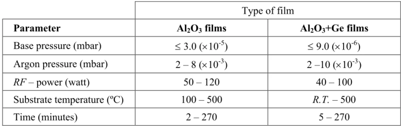
Type of film
Parameter Al2O3 films Al2O3+Ge films
Base pressure (mbar) ≤ 3.0 (×10-5) ≤ 9.0 (×10-6)
Argon pressure (mbar) 2 – 8 (×10-3) 2 –10 (×10-3)
RF – power (watt) 50 – 120 40 – 100
Substrate temperature (ºC) 100 – 500 R.T. – 500
Time (minutes) 2 – 270 5 – 270
2.1.2 Annealing
The annealing system used to anneal all the samples was the one shown on Fig.2.7. It is mainly composed by a conventional oven from TermoLab, Fornos Eléctricos LDA Company, associated to a quartz tube passing through its interior ceramic heated tube, different gas lines
Experimental procedures Materials production
connections, a pumping system composed by a rotary pump plus a diffusion pump able to reach high vacuum pressure values, and pressure gauges. The temperature inside the glass tube was controlled by a Eurotherm temperature controller (model 2216L) connected to a
Thermocoax type Kthermocouple able to reach temperatures up to 1250ºC, with an error of
0.75% above 333ºC.
To make an annealing, the samples had to be positioned inside and at the centre of the quartz tube. Before doing this, they were always placed on top of an alumina “boat” (inset of
Fig.2.7), with the thermocouple hanging on just above the samples. Usually, two to four
samples were annealed at the same time. After this, and providing that the desired pressure and atmosphere inside the quartz tube was already reached, the heating process could be
started. An average value of 30ºC.min-1 was used to increase the temperature. After the
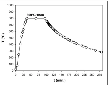
annealing time passed the oven was shut down and the samples were maintained inside the quartz tube under the same pressure and atmosphere until they reach room temperature (RT). Only in a few cases the temperature at which the samples were removed from inside the annealing quartz tube was above RT, but always below 100ºC. The representative annealing ramp used in the 800ºC/1hour annealing process is shown in Fig.2.8 as a function of time.
Fig.2.7 – Annealing system used: (a) oven, (b) thermocouple, (c) temperature controller, (d) quartz tube, (e) gas lines, (f) rotary pump, (g) diffusion pump, and (h) pressure gauges.
Experimental procedures Materials production
Fig.2.8 – Experimental annealing ramp obtained for the 800ºC/1hour annealing processes.
Different annealing conditions were performed in the as-grown films in order to improve/obtain the crystalline Ge (c-Ge) phase in the Ge doped alumina films and to try to achieve control over the Ge NCs. The deposited films were annealed at temperatures between 550ºC to 900ºC under different pressure atmospheres of air, Nitrogen, and Argon, most of which using one hour for the annealing time. While samples deposited over glass substrates were annealed at temperatures in the range of 550-580ºC, samples deposited on silicon substrates were annealed at temperatures above 800ºC. The annealing parameters of all the
annealed samples, both of Al2O3 and Ge doped Al2O3 films, are presented in Annex III. Table
2.2 presents a summary of those annealing parameters.
Table 2.2 – Summary of the annealing parameters range used in the annealing of the films.
Type of film
Parameter Al2O3 films Al2O3+Ge films
Pressure (mbar) 1000 – 8×10⁻⁶ 1000 – 8×10⁻⁶
Substrate temperature (ºC) 800 – 1000 550 – 900
Annealing time (min.) 60 – 450 60 – 240
Atmospheres Air, Argon, Nitrogen Air, Argon, Nitrogen
0 100 200 300 400 500 600 700 800 900 1000 0 25 50 75 100 125 150 175 200 225 250 275 t (min.) T ( ºC ) 800ºC/1hou
Experimental procedures Materials characterisation
2.2 Materials characterisation
After the production of the films it was necessary to proceed with their characterisation, both structural and optical. Several characterisation techniques were employed to study the properties of the produced films. A brief introduction to all the techniques that were used to characterise the produced films, including an experimental description of their use, is presented at this sub-chapter.
For the structural/chemical characterisation the main results were obtained by X-ray diffraction (XRD), Raman scattering, Rutherford Backscattering Spectrometry (RBS), Transmission Electron Microscopy (TEM) and High Resolution TEM (HRTEM). A few complementary results using X-ray photoelectron spectroscopy (XPS), Scanning Electron Microscope (SEM), and small angle diffraction (SAD) were also obtained. The optical characterisation was made by means of spectrophotometry (optical absorption spectroscopy) in the near ultraviolet–visible–infrared (NUV–Vis–IR) range and PL (photoluminescence).
2.2.1 X-ray diffraction
X-rays are electromagnetic radiation of wavelength about 1 Å, which is about the same size as an atom. They occur in that portion of the electromagnetic spectrum between gamma rays and the ultraviolet radiation. Their discovery in 1985 by Wilhelm Conrad Röntgen (Noble prize of Physics in 1901) enabled scientists to probe crystalline structure at the atomic level. Nowadays, X-ray diffraction (XRD) is one of the most important characterisation tools used in solid-state chemistry and materials science and has been in use in two main areas: for the fingerprint characterisation of crystalline materials and the determination of their structure. Each crystalline solid has its unique characteristic X-ray powder pattern, which may be used as a "fingerprint" for its identification. Once the material has been identified, X-ray crystallography may be used to determine its structure, i.e. how the atoms pack together in the
crystalline state and what the inter-atomic distance and angle are, etc. [26].In other words, the
size and shape of the unit cell for any compound can, in principle, be easily determined using the diffraction of X-rays.
An X-ray diffractometer is essentially composed of a power supply, an X-ray tube, a samples-holder, and a detector, all controlled by computer software. Two different analysis
Experimental procedures Materials characterisation
methods (geometries) can be distinguished and are frequently used in XRD measurements: the symmetrical and the asymmetrical modes.
In the symmetrical method, also known as coupled θ-2θ or Bragg-Brentano geometry,
both sample-holder and detector rotates. During the measurement process the incidence θi
angle formed between the incident X-rays direction and the sample surface plane increases step by step due to the sample-holder rotation. As the sample-holder rotates, the detector also
rotates in a coupled way, always maintaining θi = θr (known as Bragg angle). The reflection
angle, θr, is the angle defined by the sample surface plane and the detector normal direction
(see Fig.2.9).
Fig.2.9 – Schematic representation of an X-ray diffraction measurement made with Bragg-Brentano geometry.
In the asymmetrical mode, or uncoupled θ-2θ method, the samples are placed on a
sample-holder that is fixed in a certain position without rotation. While measuring, the
incident angle θi is kept constant and only the detector moves, performing the scanning along
different θr angle values. Among asymmetrical methods, glancing-angle incidence X-ray
diffraction (GIXRD) technique is the most used one. GIXRD technique, sometimes also
called grazing incidence XRD, is based in the fact that the incidence angle, θi , is a very small
fixed angle (typically 0.5º<θi≤ 3º). This fact gives GIXRD the advantage of reducing
dramatically the amount of X-ray radiation that penetrates the sample in depth. X-rays will, however, travel a bigger distance inside the film and, eventually, will not reach the substrate
X-rays beam θi θr Detector in rotation Film Substrate
Experimental procedures Materials characterisation
of the sample. Because of this, GIXRD spectra are usually more “clean” spectra, containing a lot more information about the film(s) material(s) and less information coming from the substrate. GIXRD technique is, in fact, more appropriate to the study of thin films samples then the conventional Bragg-Brentano geometry [27].
X-ray diffraction technique allowed investigating the crystallographic structure and determining the average NCs size in the films. The determination/confirmation of the crystallographic structure based on XRD is made by comparing the known lattice spacing values, d, defined on the JCPDS tables with the experimental ones, using the well known
Bragg’s Law (nλ =2dsenθ).
The shape of the diffraction peaks depends on the size and defects of the present crystallites, and the relation between peaks intensities gives information about the sample’s
texture [27]. The full width at half maximum (FWHM) of the diffraction peaks,
β
FWHM,allows the estimation of the apparent average size of the particles by using the Debye-Scherrer formula [28]:
θ
β
λ
cos 9 . 0 FWHM D= , (2.1)where D, the mean diameter of the NC, comes as a function of λ, the wavelength of the
X-ray source, θ, half of the angle between incident and diffracted beam (Bragg angle), and
FWHM
β
. The value of 0.9 is the typical value of the dimensionless shape factor, which canvaries with the actual shape of the crystallite. In order to be able to estimate the mean diameter values D of the Ge NCs on each sample, Lorentzian distribution functions fitting
each peak of the XRD spectra had to be done to obtain
β
FWHM.XRD studies involved measurements performed at three different sites. Most of them were
done at University of Minho (UM) using the Bragg-Brentano geometry. GIXRD technique
was used in measurements performed both at the Physics Department of University of Lisbon (UL), using the collaboration of Prof. Olinda Conde, and at the European Synchrotron Research Facility (ESRF) in Grenoble, France, these last made by Prof. Maria Gomes in the