Active Replication: Towards a Truly SRAM-based FPGA On-Line Concurrent
Testing
Manuel G. Gericota, Gustavo R. Alves
Department of Electrical Engineering- ISEP
Rua Dr. Ant. Bernardino de Almeida,
4200-072 Porto
− Portugal
{mgg, galves}@dee.isep.ipp.pt
Miguel L. Silva, José M. Ferreira
Dep. of Electrical & Comp. Engineering- FEUP
Rua Dr. Roberto Frias,
4200-465 Porto
− Portugal
{mlms, jmf}@fe.up.pt
Abstract
The reusing of the same hardware resources to implement speed-critical algorithms, without interrupting system operation, is one of the main reasons for the increasing use of reconfigurable computing platforms, employing complex SRAM-based FPGAs. However, new semiconductor manufacturing technologies increase the probability of lifetime operation failures, requiring new on-line testing / fault-tolerance methods able to improve the dependability of the systems where they are included.
The Active Replication technique presented in this paper consists of a set of procedures that enables the implementation of a truly non-intrusive structural on-line concurrent testing approach, detecting and avoiding permanent faults and correcting errors due to transient faults.
In relation to a previous technique proposed by the authors as part of the DRAFT FPGA concurrent test methodology, the Active Replication technique extends the range of circuits that can be replicated, by introducing a novel method with very low silicon overhead.
1. Introduction
♦
♦
♦
♦
An increasing number of systems are relying on the use of reconfigurable computing platforms to implement speed-critical computational algorithms. One of the main reasons is the possibility of reusing the same hardware when a sequence of different tasks calls for the use of different algorithms, without the need to reinitialize the system, since reconfiguration is performed without interrupting its operation. This was made possible by the introduction into the market of a new kind of
♦ This work is supported by an FCT program under contract
POCTI/33842/ESE/2000
based FPGAs (Field Programmable Gate Arrays) capable of implementing fast run-time partial reconfiguration (e. g. the Virtex family from Xilinx).
Unfortunately, the use of very deep submicron and nanometer scales in the manufacturing of larger FPGA dies increases the threat of electromigration and make them more susceptible to gamma particle radiation [1, 2]. After large periods of operation, certain defects, namely those related to small manufacturing imperfections not detected by production testing, become exposed, emerging as either stuck-at (permanent) faults or transient faults [3].
In the case of permanent faults, after faulty FPGA elements (Configurable Logic Blocks - CLBs - or routing resources) are located, the reconfiguration mechanism should be instructed to bypass them and prevent their use in future reconfigurations. Previously unused FPGA resources can replace these faulty elements, improving dependability with a very small hardware redundancy. For transient faults, on-line partial reconfiguration enables the recovery of errors in the on-chip configuration memory cells that modify the logic functionality, namely Single Event Upsets (SEU). Such upsets manifest themselves as permanent faults because of the change in functionality. However, the cause of the failure is actually transient [4].
A higher system dependability level can therefore only be achieved through the continuous testing of all FPGA resources throughout system lifetime, and by the introduction of fault tolerance features. In [5] an on-line scanning methodology to dynamically test the CLBs in an FPGA was proposed, accompanied by the evaluation of the strategy adopted to implement the rotation and test schemes. However, the success of this approach depends on the ability to replicate active CLBs, i.e. CLBs that are part of a functional block actually being used by the system. The structural testing of these CLBs is only possible if we were able to use fault-free resources to relocate their content and then release them for test, in a way that must be completely transparent for the system.
2. Background
Different off-line testing methodologies for the test of SRAM-based FPGAs, employing diverse Built-In Self--Test (BIST) strategies or external test procedures, were proposed recently in [6-13]. However, these approaches are restricted to manufacturing test, since they require the device to be off-line. This is unsatisfactory in highly -sensitive, mission-critical applications, since fault--detection latency increases greatly as a result of the off--line approach.
Trying to overcome these limitations, two on-line testing and diagnosis methods, based on a scanning methodology, were presented in [3, 14]. The main idea behind these methods is to have only a relatively small portion of the chip being tested off-line (instead of the whole chip as in previous proposals), while the rest continues its normal on-line operation. Testing is accomplished by sweeping the test functions across the entire FPGA. The functionality of a small number of FPGA elements is replicated on another portion of the device, before being taken off-line and tested. Then, another set of elements undergoes the same process, eventually spanning the whole device. However, in [3], a modification in the structure of the FPGA cells is required to implement the replication mechanism. On the other hand, in [14], the whole system must be stopped in order to replicate an entire CLB column. Since reconfiguration is performed through the IEEE 1149.1 Boundary Scan (BS) infrastructure [15], reconfiguration time is long, and it seems likely that halting the system will disturb its operation.
In [5, 16] some of the previous concepts were reused to establish an on-line FPGA testing approach that eliminated the two drawbacks mentioned before. A much smaller unit of test – the CLB – was targeted and its replication accomplished without halting the system, even when the CLB is active. However, this method was restricted to synchronous free-running clock circuits.
A new set of active replication procedures targeting the replication of synchronous and asynchronous circuits, is presented in this paper. Further to their replication function, these procedures also enable the correction of transient faults in the configuration memory. Since the IEEE 1149.1 infrastructure, is (re)used to access the FPGA configuration memory, in order to replicate and release for testing each CLB, we get the additional benefit of a reduced overhead at board level, since no other resources are used.
This approach can also be extended to the replication and release for testing of groups of interconnections. In fact, and as we shall see, handling interconnects proves to be easier than handling CLBs.
3. Replicate and release for testing
Dynamically replicating an active CLB is not just a matter of relocating its functional specification: the corresponding interconnections with the rest of the circuit have to be established; additionally, internal state information has to be copied as well, depending on the functionality it is implementing. This task is not trivial due to two major issues: i) configuration memory organization, and ii) internal state information.
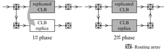
The configuration memory is partitioned into one-bit wide vertical frames grouped into larger units called columns. To each CLB column corresponds a configuration column, with multiple frames, which mixes internal CLB configuration and state information, and column routing and interconnect information. The configuration process is a sequential mechanism that spans through some (or eventually all) CLB configuration columns. When replicating an active CLB more than one column may be affected, since its input and output signals (as well as those in its replica) may cross several columns before reaching its source or destination. Any reconfiguration action must therefore ensure that the signals from the replicated CLB are not broken before being totally re-established from its replica, otherwise its operation will be disturbed or even halted. Furthermore, the functionality of the CLB replica must be perfectly stable before its outputs are connected to the system to avoid output glitches. The only viable solution is to divide the replication process in two phases, as illustrated in figure 1. 1st phase 2nd phase - Routing array replicated CLB CLB replica replicated CLB CLB replica
Figure 1. Two-phase CLB replication process
In the first phase, the internal configuration of the CLB is replicated and the inputs of both CLBs are placed in parallel. Due to the low-speed characteristics of the reconfiguration (BS) interface, the reconfiguration time is relatively long when compared with the system speed of operation. Therefore, in the second phase, when the outputs of the CLB replica are connected to the circuit, they are already perfectly stable.
Notice that rewriting the same configuration data does not generate any transient signals, so this process does not affect the remaining resources covered by the rewriting of the configuration frames that are needed to carry out the replication.
Another major requirement for the success of the replication process is the correct transferring of state
information. If the CLB is currently implementing a sequential function, the internal state information must be preserved and no writes could be lost during the copying process. The solution to this problem depends on the type of implementation. In this paper we shall consider three implementation cases: synchronous free-running clock circuits, synchronous gated-clock circuits, and asynchronous circuits.
When dealing with synchronous free-running clock circuits, the two-phase replication process described earlier is a good solution. Between the first and the second phase, the CLB replica has the same inputs as the replicated CLB and all its four flip-flops (FFs) acquire the state information. Notice that this is true even when dealing with asynchronous circuits if the longest “update period” is higher than the time interval between first and second phases.
Despite the effectiveness of this solution, its restriction to synchronous free-running clock circuits is a serious limitation. A broad range of circuits uses gated-clocks, where input acquisition by the FF is controlled by the state of the clock enable signal. As we cannot ensure that this signal will be active between the first and the second phrase of the replication process, it is uncertain that the CLB replica will capture the state information. On the other hand, it is not feasible to set this signal as part of the replication process, because the value present at the input of the replica FFs may change in the meantime, and a coherency problem will then occur.
To solve this problem we used a replication aid block, which manages the transfer of the state value from the replicated FFs to the replica FFs, while enabling their update by the circuit at any instant, without delaying the replication process. The whole replication scheme is represented in figure 2, where only one logic cell is shown, for reasons of simplicity. Each CLB comprises four of these cells, which can be considered individually for the purpose of implementing this procedure. The temporary transfer paths established between the replicated and the replica cell do not affect their functionality, since they use only free routing resources and do not modify their structure.
The 2:1 multiplexer present in the replication aid block is controlled by the clock enable signal (CE) of the replicated FF. If this signal is not active, the output of the replicated FF (FF_OUT) is applied to the input of the replica FF, through a multiplexer controlled by the bypass control signal (BY_C). A clock enable signal, generated by the replication aid block (capture control signal - CC), forces the replica FF to hold the transferred value. The replica FF acquires the state information present in the replicated FF. If the CE signal is active or is activated during this process, the multiplexer selects the LOGIC_OUT signal and applies it to the input of the
replica FF, which is updated at the same time and with the same value as the replicated FF, guaranteeing state coherency. Figure 3 represents the flow diagram describing the replication process. Figure 4 shows the waveform simulation of state transfer and update operations during the replication process. No loss of information or functional disturbance is observed during the process. D Q CC 1 0 Replication aid block CE CLK RESET to the circuit from the circuit LOGIC_OUT FF_OUT D Q CE R BY_C 0 1 Replica cell [A1...A4] O LUT D Q CE R Replicated cell [A1...A4] O LUT
Figure 2. Synchronous gated-clock circuit replication scheme
Begin
Connect CEs and the temporary transfer signals FF_OUT and LOGIC_OUT to the replication
aid block, and place the remaining input signals in
parallel BY_C="HIGH"
CC="HIGH"
CC="LOW"
Place in parallel the CE inputs of both logic cells Disconnect all signals from
the replication aid block Place the outputs of both logic cells in parallel
Disconnect the inputs of the replicated logic cell
End > 2 CLK pulse N S >1CLK pulse N S BY_C="LOW"
Disconnect the outputs of the replicated logic cell
Figure 3. Flow diagram of the replication process
State tranferring process The state is acquired by the replica ff The state is updated by the circuit replica ff state replicated ff state
Figure 4. Simulation of a state transfer and update during the replication process
The control signals CC and BY_C are configuration memory bits whose values are driven through
reconfiguration of the configuration memory. BY_C directs the state signal to the input of the replica FF, while CC enables its acquisition. It is therefore possible to control the whole replication process through the BS infrastructure, and as such no extra FPGA pins are required. The CC net includes the FF shown in figure 2, which is there simply as a consequence of the structure of the CLB slice, and does not play any role in the process.
After the state has been transferred, the input signals involved in the process are placed in parallel, all the signals to and from the replication aid block are disconnected, and the outputs are also placed in parallel. After at least one clock cycle the replicated block is disconnected and could be tested. Each of these steps (corresponding to a square in the flow diagram shown in figure 3) implies a new reconfiguration file. A total of 9 files are needed to accomplish the replication, instead of 3, as would only be necessary when dealing with purely combinational or synchronous free-running clock circuits. However, in most cases, their size is much smaller. To change the value of CC and/or BY_C only one configuration frame is needed, which is around 2 Kbit (220 µs for a 20 MHz BS test frequency).
Practical experiments performed using a Virtex XCV200 from Xilinx [17] over the ITC’99 Benchmark Circuits from the Politécnico di Torino [18] demonstrated the effectiveness of our approach. The average number of bits needed to replicate each CLB using this strategy, including configuration and command frames, was around 230 Kbit. At an operation frequency of the BS infrastructure of 20MHz, the mean time for a complete replication of a CLB was 24 ms. Therefore, the replication of all CLBs of a XCV200 device (array size =28x42=1176 CLBs) will require 28 seconds, with only one CLB replicated at a time.
This approach is also applicable to multiple clock/multiple phase circuits, since only one clock signal is involved in the replication process at a time (provided that the slowest “clock” period is higher than the duration of the replication process), and with asynchronous circuits, where transparent data latches are used, instead of FFs. In this case, the register present in the replication aid block may be configured also as a latch, instead as a FF, if this is preferred or if no adequate clock signal is available.
The same two-phase procedure is effective on the replication and release for testing of local and global active interconnections. The interconnections to be replicated are first duplicated in order to establish an alternative path, and then disconnected, and made available for test.
The extension of this on-line replication concept to the replication of Look-Up Tables (LUTs) configured as RAMs is not viable, despite their content could be read and written through the configuration memory. If there is a
write attempt during the replication interval, there is no feasible way, other than to stop the system, capable of ensuring the coherency of the values, as stated in [4]. Furthermore, since frames span an entire column of CLB slices, the same LUT bit in all of them is updated with a single write command. We must ensure that either all the remaining data in the slice is constant, or it is also modified externally through partial reconfiguration.
Notice that more than one CLB could be replicated at each time, improving the scalability of the process, which is an important issue if we are dealing with larger FPGAs.
4. Fault detection and error recovery
Since the replication procedure used with synchronous free-running clock circuits did not perform a true state transfer operation, but rather an acquisition of the values present at the inputs of the replica CLB FFs, the acquired state information is correct, despite any fault that may affect the replicated CLB FFs. As a consequence, and after the replication process, the outputs of the CLB replica always display the correct values, automatically correcting any faulty behavior. On the other hand, when replicating synchronous gated-clock circuits (or asynchronous circuits), a truly state transfer operation is executed, so if a permanent fault in the replicated CLB affects the value held by the FF(s) (or latches), this fault is propagated to the replica CLB and will remain active until an update occurs. The fault in the replicated CLB will be detected during the subsequent test phase and it will be flagged as defective, meaning that it will not be used again in a later reconfiguration.
Depending on the method used to create the reconfiguration files, the replication procedure can also recover from errors caused by transient faults in the on--chip configuration memory cells that modify the logic functionality. A typical example of such errors is SEUs in space environments. Since Virtex FPGAs enable readback operations, a completely automatic read-modify-write procedure could be implemented to replicate the CLBs using local processing resources. In this case, any transient fault in the configuration memory is propagated and will affect the functionality of the CLB replica. On the other hand, if the reconfiguration files are generated from the initial configuration file stored in an external memory, any error due to SEUs is corrected when the affected blocks are replicated.
The previous successful testing of the CLB replica ensures its good functionality, but the replicated CLB might be faulty. When the inputs and outputs of both CLBs are placed in parallel, we may be interconnecting nodes with different voltage levels. Due to the impedance of the routing switches, this apparent “short-circuit” behaves as a voltage divider, limiting the current flow in
the interconnection. Therefore, no damage results to the FPGA, as proved by extensive experimental essays. Since we are dealing with digital circuits, the analogue value resulting from the voltage divider leads to a well defined value (logic 0 or logic 1) when it goes through a buffer along the routing, or at the input of the next CLB or Input/Output Block (IOB). No logic value instability was reported during the essays.
Each CLB comprises, in addition to its logic resources, three routing arrays: two locals (input and output) and one global. The routing resources in these arrays may be unidirectional or bi-directional, as indicated in figure 5. No routing resources are available in the local arrays to establish direct interconnections with other CLBs, so those required by the replication process can only be established through the global routing array.
Input routing array Output routing array
Slice 1 CLB
Global routing array
Slice 1
Figure 5. CLB routing arrays resources
Between local and global routing arrays only unidirectional routing resources are available. Since no fault at any of the replicated CLB inputs, due to that unidirectionality, will propagate backwards, the logic values present at the inputs of the replica CLB are not affected by the interconnection, even if the replicated CLB is faulty. As such, all CLB replica inputs will always reflect the correct values.
This is also true when replicating active interconnections where faults in the replicated net are automatically corrected when the replication takes place.
6. Conclusion
This paper presented a set of procedures to replicate and release for test all FPGA resources, including those being used by the application currently running. These procedures are entirely non-intrusive and enable the implementation of truly on-line testing strategies, while at the same time correcting errors caused by transient faults. The reusing of a standard test infrastructure to access the configuration memory avoids the need for extra pins.
Taking advantage of the novel partial and dynamic reconfiguration features of recent FPGA devices, this set of procedures helps to improve the dependability of reconfigurable hardware systems in a way that is completely transparent to the system operation.
7. References
[1] F. Hanchek, S. Dutt, “Methodologies for Tolerating Cell and Interconnect Faults in FPGAs”, IEEE Trans. on Computers, Vol. 47, No. 1, pp. 15-33, Jan. 1998.
[2] J. Lach, H. W. Mangione-Smith, M. Potkonjak, “Low Overhead Fault-Tolerant FPGA Systems”, IEEE Trans. on VLSI Systems, Vol. 6, No. 2, pp. 212-221, June 1998.
[3] N. R. Shnidman, H. W. Mangione-Smith, M. Potkonjak, “On-Line Fault Detection for Bus-Based Field Programmable Gate Arrays”, IEEE Trans. on VLSI, Vol. 6, No. 4, pp. 656-666, Dec. 1998.
[4] W. Huang, E. J. McCluskey, “A Memory Coherence Technique for Online Transient Error Recovery of FPGA Configurations”, Proc. 9th ACM Intl. Symp. FPGA, pp. 183-192,
Feb. 2001.
[5] M. G. Gericota, G. R. Alves, M. L. Silva, J. M. Ferreira, “DRAFT: An On-Line Fault Detection Method for Dynamic and Partially Reconfigurable FPGAs”, Proc. 7th IEEE Intl. On-Line
Testing Workshop, pp. 34-36, July 2001.
[6] C. Stroud, S. Konala, P. Chen, M. Abramovici, “Built-In Self-Test of Logic Blocks in FPGAs (Finally, A Free Lunch: BIST Without Overhead!)”, Proc. 14th IEEE VLSI Test Symp.,
pp. 387-392, April 1996.
[7] C. Stroud, E. Lee, M. Abramovici, “BIST-Based Diagnostic of FPGA Logic Blocks”, Proc. Intl. Test Conf., pp. 539-547, Nov. 1997.
[8] C. Stroud, S. Wijesuriya, C. Hamilton, M. Abramovici, “Built-In Self-Test of FPGA Interconnect”, Proc. Intl. Test Conf., pp. 404-411, Nov. 1998.
[9] W. K. Huang, F. J. Meyer, X. Chen, F. Lombardi, “Testing Configurable LUT-Based FPGA's”, IEEE Trans. on VLSI, Vol. 6, No. 2, pp. 276-283, June 1998.
[10] W. K. Huang, F. J. Meyer, F. Lombardi, “An approach for detecting multiple faulty FPGA logic blocks”, IEEE Trans. on Computers, Vol. 49, No. 1, pp. 48-54, Jan. 2000.
[11] T. Inoue, S. Miyazaki, H. Fujiwara, “Universal Fault Diagnosis for Look-up Table FPGAs”, IEEE Design and Test of Computers, Vol. 15, Nº 1, pp. 39-44, January-March 1998. [12] M. Renovell, J. M. Portal, J. Figueras, Y. Zorian, “RAM-Based FPGA's: A Test Approach for the Configurable Logic”, Proc. DATE Conf., pp. 82-88, February 1998.
[13] M. Renovell, J. M. Portal, J. Figueras, Y. Zorian, “Testing the interconnect of RAM-based FPGAs”, IEEE Design and Test of Computers, Vol. 15, Nº 1, pp. 45-50, January-March 1998. [14] M. Abramovici, C. Stroud, S. Wijesuriya, C. Hamilton, V. Verma, “On-Line Testing and Diagnosis of FPGAs with Roving STARs”, Proc. 5th IEEE Intl. On-Line Testing Workshop, pp.
2-7, July 1999.
[15] IEEE Std. Test Access Port and Boundary Scan Architecture (IEEE Std. 1149.1), IEEE Std, Board, May 1990. [16] M. G. Gericota, G. R. Alves, M. L. Silva, J. M. Ferreira, “Dynamic Replication: The Core of a Truly Non-Intrusive SRAM-based FPGA Structural Concurrent Test Methodology”, 3th IEEE Latin-American Test Workshop, pp. 70-75, Feb. 2002.
[17] The Programmable Logic Data Book, available at http://www.xilinx.com
[18] Politécnico di Torino ITC’99 benchmarks, available at http://www.cad.polito.it/tools/itc99.html