UNIVERSIDADE DE LISBOA FACULDADE DE CIÊNCIAS
DEPARTAMENTO DE ENGENHARIA DA GEOGRAFIA, GEOLOGIA E ENERGIA
Development and Evaluation of a Low-Cost Dynamic Illumination
Setup for Advanced Photovoltaic Modules Performance Testing
Nuno André Reis e Ruas
Trabalho realizado sob a supervisão de
Orientador: Miguel Centeno Brito (Universidade de Lisboa) Co-orientador: Francky Catthoor (imec)
Mestrado Integrado em Engenharia da Energia e Ambiente Dissertação
Abstract
Current solar simulators only focus on steady-state or pulsed (flasher) irradiance conditions, under standard test condition, to measure peak performance of photovoltaic (PV) modules. For realistic scenarios other more dynamic conditions are needed, such as lower irradiance levels that change over time and shading patterns (from clouds and surrounding objects). This work presents of a low-cost indoor dynamic illumination setup to test smart PV modules under dynamic conditions of irradiance to evaluate its performance, allowing temporal and spatial irradiance variation. This setup is be able to simulate conditions close to realistic outdoor patterns enabling. For example, to simulate irradiance conditions in countries such as Belgium with highly variable irradiance which changes constantly in space and time.
The dynamic illumination setup has a test area of 1.6x1 m2 (large enough to work with a standard size PV module). The distance of the test area to the LED lamps varies from 100 mm to 600 mm relative to the light source. Also, it allows to change its angle (from -40o to 400, at 600mm from the lamps, relative to the horizontal position) to simulate different incident angles of light. The light source is totally based on LED technologies, composed of 66 LED lamps with 22 W each, which have a spectrum between 400 nm and 800 nm. The setup uses mirrors and in this way achieves Class C for non-uniformity of irradiance according to IEC 60904-9. The average irradiance varies from 120 W/m2 (at 600 mm from the lamps) to 156 W/m2 (at 100 mm from the lamps). The dynamic illumination design results from a he trade-off between cost, uniformity and maximum irradiance.
Index
Abstract ... i
Figure Index ... iii
Table Index ... iv Acknowledgment ... v 1 Introduction... 1 2 Concepts ... 1 2.1 Radiation... 1 2.1.1 Electromagnetic radiation ... 1 2.1.2 Black body ... 2 2.1.3 Solar irradiance ... 2 2.2 Photovoltaics ... 5 2.2.1 PN junction ... 5
2.2.2 Silicon crystalline photovoltaic cell ... 7
2.2.3 Photovoltaic module ... 9
2.3 Solar simulator... 10
2.3.1 Standard test conditions ... 10
2.3.2 IEC 60904-9: Solar simulator performance requirements ... 11
2.4 Belgium’s climate conditions ... 11
3 Dynamic Illumination Setup ... 12
3.1 Dynamic Illumination Setup Requirements ... 13
3.2 Mechanical design ... 14
3.3 Illumination ... 15
3.4 Light Source ... 18
3.5 Light source control ... 20
3.6 Irradiance and irradiance uniformity ... 22
3.7 Future development ... 25
4 Conclusion ... 25
5 References... 26 Attachment 1 – Code for the Graphic User interface to control the dynamic illumination Setup ... I Attachment 2 – Code for the Arduino’s to control the dynamic illumination setup ... III Attachment 3 – Dynamic illumination setup upgrade 1 ... VII Appendix A – Design and construction of a temperature measurement system ... IX Appendix B – Wind tunnel measurements ... XII
Figure Index
Figure 1 – Electromagnetic radiation spectrum [3] ... 1
Figure 2 – EM spectrum of the sun. In green represents the EM spectrum before entering the atmosphere and in blue after entering the atmosphere [4] ... 4
Figure 3 – Illustration of the air mass depending on the incident angle of the sun’s irradiance ... 4
Figure 4 – Difference between a metallic, insulator and semi-conductor material ... 5
Figure 5 – Effect of the temperature in a semi-conductor on its charge carries ... 5
Figure 6 – Types of doping of a semi-conductor ... 6
Figure 7 – Energy pf a photon required to for an electron to go from the valence band to the conductive band 6 Figure 8 – Representation of a PV Junction [5] ... 7
Figure 9 – representation of a cross section of a PV cell... 7
Figure 10 – IV curve of a PV cell ... 8
Figure 11 – Effect of the series resistance and the shunt resistance on a typical IV curve of a PV cell ... 8
Figure 12 – Effect of the temperature and irradiance on a typical IV curve of a PV cell ... 9
Figure 13 - Representation of a PV module and its elements... 9
Figure 14 – Representation of the function of a by-pass diode and how it redirects the current from a shaded PV cell. ... 10
Figure 15 – Illumination in Ghent (BE) at 19-04-2013, of a period of 15 min with fast varying illumination [7] ... 12
Figure 16 – Average global irradiance (and its diffused component) of Belgium in fixed horizontal planed (south oriented) and for a solar tracking plane. This values were obtain in PVGis [8]. ... 12
Figure 17 – Front side of the dynamic illumination setup ... 15
Figure 18 – Rear side of the dynamic illumination setup ... 15
Figure 19 – LED lamps disposition inside to illumination setup ... 16
Figure 20 –Schematic of the electrical circuit of the LED lams and LED control ... 17
Figure 21 – Electrical Box with LED drivers ... 18
Figure 22 – SMD 2835 LED spectrum irradiance measured by a spectrometer at a distance of 10mm. Comparison with the AM0 and AM1.5 spectrum irradiance. ... 18
Figure 23 – Schematic of the electrical circuit of the LED lamps ... 19
Figure 24 – Spectrum reflectivity measurement for a standard mirror ... 19
Figure 25 – Schematic drawing of the electrical circuit of the Arduino’s shield to convert a 5V PWM to a 10V PWM signal ... 21
Figure 26 – GUI to control the lamps brightness ... 22
Figure 27 – Irradiance [W/m2] and uniformity for the test area (1x1.6m2), for different distances from the light source. The measurements presented in the chart were taken with the lamps at full power and for different height. ... 24 Figure 28 – GUI for the Dynamic Illumination Control... I Figure 29 – PCB for the new Arduino Shield to control PWM signal ... VII Figure 30 – Electrical schematic for the new PWM signal control ... VIII Figure 31 - Type K thermocouples schematic ... IX Figure 32 – Recommended schematic for the AD595CQ and type K thermocouple. ... IX Figure 33 – PCB design for the AD595CQ and type K thermocouple. Yellow lines correspond to the top layer of the PCB and the orange lines correspond to the bottom layer of the PCB ... X Figure 34 – GUI for the temperature measuring system. ... X Figure 35 – Schematic representation of the PV module used in the wind tunnel measurements. The module has 6 mono-crystalline PV cells. 12 temperature points are used to the temperature profiling of the PV module. The temperature point 1 and 2 are used as a reference for the ambient temperature (they are placed inside the wind tunnel but are isolated form the wind flow). ... XII
Table Index
Table 1 – Definition of solar simulator classification ... 11 Table 2 - Highlights of the requirement established for the dynamic illumination setup ... 13 Table 3 – Minimum, maximum and average irradiance values measured on the test area (1x1.6m2) and the non-uniformity index for each height ... 23 Table 4 – Lamp and LED driver specification ... VII
Acknowledgment
To my advisor and professor, Miguel Brito I would like to thanks for all his comments and useful insight that allowed this master thesis to come to light. Furthermore, my sincere thanks to Francky Catthoor, who provided me the opportunity work on this project and to join imec as an intern.
A special thanks goes to Didier Dehertoghe who helped me with his remarks and experience in the development of this project. I would also like to thanks my colleagues Jonathan Govaerts and Hans Goverde for their support on this long journey.
I gratefully acknowledge the financial support of the Flemish Government in the frame of the IWT-SBO project Smart PV (#110025).
1 Introduction
The work of this master thesis has been executed within the framework of an internship at imec. The PV module
technologies group at imec needed to develop a low-cost illumination equipment to test a new smart photovoltaic
(PV) module technology [1]. This illumination setup should be able to operate with large-area (1.6x1 m2) PV modules in order to more accurately evaluate panels in conditions that are closed to reality [2]. Concretely, it is required to be able to illuminate at lower irradiance levels that can vary dynamically in time and with the best cost-effective spatial non-uniformity as possible.
During this internship there were other collaborations in other projects, such as the wind tunnel measurements (measure the temperature profile of scaled down PV modules made with 6 cells in series for several wind speeds and inclinations) and the Sky imager project (following cloud movement in the sky and predict their path over a short period of time). These projects are summarized in the annexes to this dissertation.
The thesis is structured as follows. Section 2 gives a brief overview of all the concepts explored in this thesis. Section 3 presents the relevant development stages of the dynamic illumination setup, including design, construction and development of the dynamic illumination setup. The main conclusions and future outlook are discussed in Section 4. The attachments described technical details of the set-up. The annexes describe side projects that were performed during the internship at imec but which are not directly related to the main core of the thesis.
2 Concepts
The proposed dynamic illumination development involved several areas in which this section is going to introduce. The main purpose of Section 2.1 is to explain solar irradiance and what it is and what it quantifies. Section 2.2 describes the photovoltaic (PV) devices used to transform the solar irradiance into electricity and how it is characterized. Next, the tool do evaluate these devices is presented. The last section presents an overview of how the Belgium weather conditions affect the solar irradiance and how this reduces the energy yield of PV modules.
2.1 Radiation
2.1.1 Electromagnetic radiation
Radiation is how energy is emitted in form of wave or particle (photons) through a mean (in this case, space). Energy reaches the Earth mostly from the Sun in the form of electromagnetic radiation. The energy carried by the photon can be characterized by its wavelength (λ) or its frequency (ν). Electromagnetic radiation extends in a broad spectrum, has shown Figure 1.
A photon has an amount of energy which is inversely proportionate to its wavelength. This energy can be calculated using:
𝐸[𝑒𝑉] =
ℎ[𝐽.𝑠].𝑐[𝑚 𝑠⁄ ] λ[μm]=
1.24 λ (1)where h is Planck constant and c is the speed of light.
For each radiation spectrum it is possible to determine the spectral irradiance by:
𝐹(𝜆)[𝑤 (𝑚
⁄
2. 𝜇𝑚)
] = 𝜙. 𝐸.
1Δ𝜆 (2)
where Φ is the photon flux or the number of photons per square meter per second:
𝜙 =
𝑛𝑢𝑚𝑏𝑒𝑟 𝑜𝑓 𝑝ℎ𝑜𝑡𝑜𝑛𝑠𝑚2.𝑠 (3)
To know the radiant power density or irradiance over the entire spectrum emitted by a specific body it is necessary to integrate the spectral irradiance:
𝐻[𝑊 𝑚
⁄
2] = ∫ 𝐹(𝜆) 𝑑𝜆
0∞ (4)2.1.2 Black body
A black body is defined as ideal radiation absorber. A black body in thermal equilibrium is also a perfect emitter for every wavelength. This means that it emits more energy than any other body at the same temperature and, on the other hand, it diffuses that radiation isotopically.
The Spectral irradiance of a black body is given by Planck’s law when it is in thermal equilibrium at a defined temperature:
𝐹(𝜆)[𝑤 (𝑚⁄ 2. 𝜇𝑚)] = 2𝜋.ℎ.𝑐2 𝜆5(𝑒𝑘.𝜆.𝑇ℎ.𝑐−1)
(5)
where T corresponds to the temperature of the black body in Kelvin .
By integrating the Planck’s law results the Stefan-Boltzmann law that determines the irradiance of the black body:
𝐻𝐵𝐵 = 𝜎[𝑊 (𝑚⁄ 2. 𝐾4)]. 𝑇4 (6)
where σ is the Stefan-Boltzmann constant.
2.1.3 Solar irradiance
Solar radiation originates in the Sun’s core where a fusion reaction takes place, merging two atoms of hydrogen into one of helium, realising energy in the process. Part of this energy is converted into heat and part is emitted as a photon. Every photon after being released makes its way up to the Sun’s surface (taking many thousands of years). On the surface this photons are ejected and are be quantified by the irradiance (power per square metre).
The irradiance emitted by the Sun at its surface may be described as a black body at the same temperature. An approximation of irradiance of the Sun can be given by:
𝐻𝑆𝑢𝑛= 𝜎𝑇4= 6.4 × 10⁷ 𝑊/𝑚2 (7)
where T ≅ 5800 K is the temperature of the Sun’s surface.
Only a fraction of these photons reach Earth. The fraction of energy that reaches Earth is a function of the radius of the sun and the distance between the two bodies, given by the following expression:
𝐻0= 𝑟2
𝑑2𝐻𝑆𝑢𝑛 ≅ 1393.8 𝑊 𝑚⁄ 2 (8)
where the r = 7x10 5 km is the radius of the Sun and d = 1.5×10⁸ km is the distance from the Sun to the Earth.
The Sun’s irradiance enters the Earth atmosphere in the form of a direct beam of radiation. As it crosses the atmosphere it will suffer interference from its elements. This interference reduce the irradiance and changes its spectrum. Some of the reasons are:
Atmospheric gases such as Ozone (O3), water vapour (H2O) and carbon dioxide (CO2) have high absorption of photon with certain wavelength (their effect can be seen in
Figure 2)
Other air gases and dust in the atmosphere also absorb photon but mainly scatters them (diffuse light) The above effects depend greatly on the distance that the photons have to travel (in the atmosphere) to reach the Earth surface. This effect is characterized as the Air Mass (AM). The AM is a measure of the reduction in the power of the radiation as it passes through the atmosphere. Figure 2 quantifies the effect of the one and half AM on the spectral irradiance.
Figure 2 – EM spectrum of the sun. In green represents the EM spectrum before entering the atmosphere and in blue after entering the atmosphere [4]
The AM can be calculated by the following expression is used:
𝐴𝑀 =
1cos 𝜃 (9)
where θ is the incident angle which is the angle between the beam radiation direction and the earth surface, as shown in Figure 3.
Figure 3 – Illustration of the air mass depending on the incident angle of the sun’s irradiance
The θ is dependent on the location, time and the position of the target. A close approximation, for a clear sky, of the effect of the AM on the direct of the irradiance can be given by:
𝐻𝐷= 𝐻0× 0,7𝐴𝑀 0,678
(10)
For AM1.5 the irradiance is defined as 1000W/m2.
H2O H2O
O2
2.2 Photovoltaics
Photovoltaics is a process of converting direct solar irradiance into electricity, which can be achieved by using semiconductors. A device with this capability is a photovoltaic (PV) cell (based on a PN junction) that when connected to an external load produces a flow of electrons (or current). These devices can be joined in series and in parallel to form PV modules.
2.2.1 PN junction
A semi-conductor can only conduct electricity in certain conditions, this means that electrons can only go from the valence band to the conductive band they are provided enough energy.
Figure 4 – Difference between a metallic, insulator and semi-conductor material
Valence Band: is the outer shell of an atom where its highest energy electrons are present
Conduction Band: higher level than the valence band were electrons are consider free from the atom Band Gap: difference of energy between the valence and conduction band (Figure 4)
Fermi level: The Fermi level and band gap in a solid largely determine its electrical properties. In a perfect semiconductor (in the absence of impurities/dopants), the Fermi level lies close to the middle of the band gap (Figure 4)
Charge carriers or electron-hole, is the absences of and electron in an otherwise full valence band, depending on the type of material or type or doping
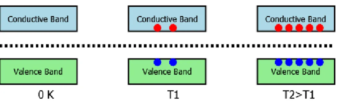
Semiconductors are sensitive to temperature. As shown in Figure 5Error! Reference source not found., as the temperature goes up the number of pares electron-holes also go up, meaning that the material gets higher conductivity
Figure 5 – Effect of the temperature in a semi-conductor on its charge carries
The most common semiconductor for PV application is silicon. Silicon in its intrinsic form at T= 0 K has no free electrons because the 4 valence electrons make covalent bonds with their neighbours.
Doping is used to change the electric properties of a semiconductor such has silicon, by increasing their charge carriers, thus increasing the conductivity of silicon. Doping consist of adding impurities into the material’s crystalline structure, as shown in Figure 6. For the case of silicon, two types of doping1 are used:
N-doped silicon: To accomplish this phosphorous (P) is used because it contains 5 valence electrons, which creates a covalent bond with the atoms of silicon leaving one free electron.
P-doped silicon: For this case Boron (B) is used because it has only 3 valence electrons that will try to create a covalent bound with silicon but in the process creates one hole.
Figure 6 – Types of doping of a semi-conductor
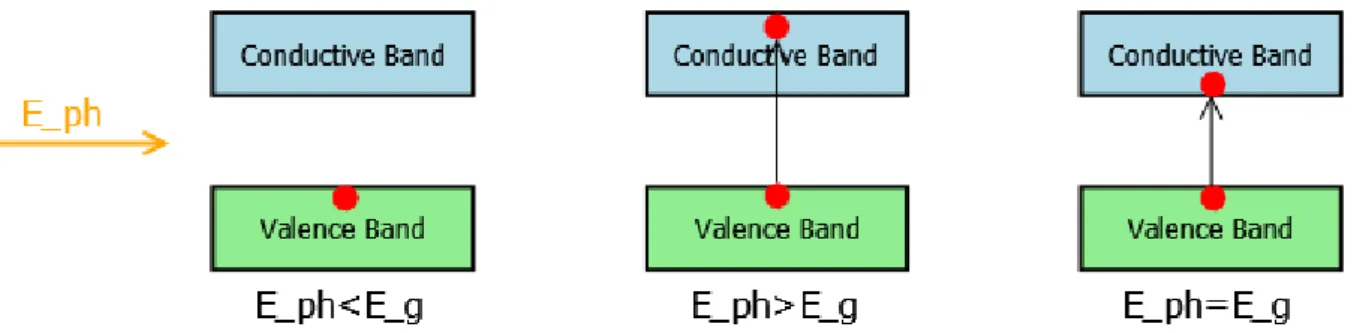
One important characteristic of silicon, like other semiconductors, is the ability to absorb incident photons, between the wavelength ranges of 300 nm and1200 nm. When a photon is absorbed by silicon three situations can occur:
If the energy of the photon (Eph) is less than that of the energy band gap (Eg) no pair electron-hole will
be created (Figure 7)
If the Eph is greater than that of the Eg the photon will be absorbed, part of the energy will be used to
create the charge carrier and the excess will be released as heat (Figure 7)
If the Eph is equal to that of the Eg the photon will be absorbed and all the energy will be used to make
the electron transit to the conduction band (Figure 7)
Figure 7 – Energy pf a photon required to for an electron to go from the valence band to the conductive band
The PN junction is formed by combining an n-type and a p-type semiconductor, as illustrated in Figure 8. When the junction of the two materials becomes depleted of electron-hole pairs, this creates a moderate energy field, permitting a reduced electron and hole diffusion. The electric field created can be externally manipulated by applying a voltage using an external circuit, in two different ways:
1 There a several material that can be used for doping silicon. For N-doped any atom from the group V of the periodic table
can be used. For the P-doped any atom from the group III of the periodic table can be used. From the purpose of this work only P (group V) and B (group III) will be mention.
Forward bias: By applying a positive voltage to p-doped side and a negative voltage to n-doped side the electric field diminishes, increasing the diffusion, thus allowing the electrons to flow in one direction creating a current. This is the basic functionality of a diode.
Reversed bias: by reversing the polarity the opposite happens, the electric field increases and the diffusion diminishes. Thus electrons and holes are pulled away from the junction.
Figure 8 – Representation of a PV Junction [5]
The PN-junction with reversed bias is the main principle behind the silicon crystalline PV cell. This can be used as a simplified model to understand itsoperation.
2.2.2 Silicon crystalline photovoltaic cell
A PV cell is an electronic device that directly converts irradiance into electricity. This process is based on a PN junction which creates a voltage between a p-doped and the n-type Si and promoting a current flow on an external circuit. Figure 9 shows a cross section of a typical solar cell.
Figure 9 – representation of a cross section of a PV cell
To characterize the electrical behaviour of a PV cell several parameters are needed, such as: Short circuit current, Isc: is the maximum current possible when the voltage is zero
Open circuit voltage, Voc: is the maximum voltage possible when the current is zero
Maximum power, Pmax: is maximum power that it is able to produce at Vmp and Imp
Fill factor, FF: ratio between the area of Isc and Voc and the area of Imp and Vmp
Efficiency, η: is the fraction of incident power which is converted to electricity
𝜂 [%] =
𝐼𝑠𝑐𝑉𝑜𝑐𝐹𝐹𝑃𝑖𝑛
× 100
Characteristic resistance, Rch: the resistance at the MP
Series resistance, Rs: resistance of the metal contact of the PV cell.
Shunt resistance, Rsh: resistance of the caused by manufacturing defects
All of these can be taken from the measurement of the IV curve of a solar cell, relationship between the current produce by the PV cell and the corresponding voltage. A typical IV curve is shown in Figure 10.
Figure 10 – IV curve of a PV cell
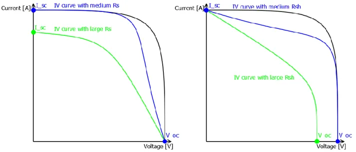
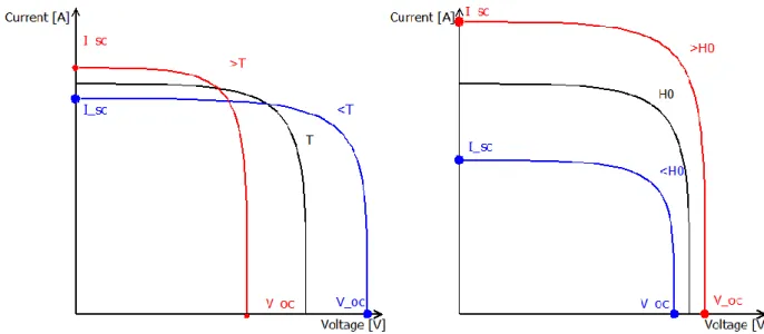
The parameters of a PV cell can be affected by internal and external factors. Internally, the series resistance Rs
affects mainly the Isc but also slightly the Voc. The shunt resistance Rsh affect mainly the Voc and slightly the Isc.
Figure 11 shows a representation of this effect.
Figure 11 – Effect of the series resistance and the shunt resistance on a typical IV curve of a PV cell
Externally, there are two factor in play that affect the IV curve of a PV cell: the temperature of the cell and the irradiance. As the temperature increases the Voc decreases but the Isc increases slightly. If the temperature
decreases the Voc increases and Isc decreases slightly. For the irradiance, as it increases, both Voc and Isc increase
(Isc increases much more than the Voc) and if it decreases Voc and Isc decrease (Isc decreases much more than the
Figure 12 – Effect of the temperature and irradiance on a typical IV curve of a PV cell
2.2.3 Photovoltaic module
PV modules are made of PV cells connected to each other to increase energy output. A typical c-Si PV cell produces around 0.6V (at 25oC and at AM1.5 irradiance) and 8.5A (156x156mm2 area). One cell has limited voltage and cannot be used in many application. To overcome this PV cells are connected in series (to increase voltage) and in parallel (to increase the current) to form modules. This allows to raise to output to values that are useful.
A PV module is made from several components (Figure 13), each with a specific function:
High transmissivity glass (special made glass with low iron content) to allow mechanical rigidity and protection without affecting the effectiveness of the PV cells;
Encapsulate to protect PV cells against outside conditions and to provide an adhesive surface to the glass. A typical material used is Ethyl Vinyl Acetate (EVA);
Back sheet for further protection from the environment;
Aluminium frame for extra rigidity and to allow the module to be mounted in a PV system;
Junction Box (can include a by-pass diode) connects all the leads from the PV cells and it is where the external connections are.
Figure 13 - Representation of a PV module and its elements
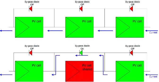
An important limitation of PV modules today is the way the strings of solar cells are connected in the module. If one of the cells in a string is partially or fully shaded the current it produces will decrease, affecting the entire
string current output. The shaded cell will dissipate the current produced by those unshaded forming hotspots. This will reduce the performance of the entire PV module and diminish the energy yield.
Figure 14 – Representation of the function of a by-pass diode and how it redirects the current from a shaded PV cell.
One way to partly overcome the effect of shading on the modules and to reduce hotspots is the use of by-pass diodes. Figure 14 shows the functionality of a by-pass diode. The current flows in the normal circuit in an unshaded string. On the other hand, if one of the strings is shaded the current flows through the by-pass diode, introducing a small voltage drop but keeping the current from the other cells. The by-pass diode can be used with only one cell, with groups of cells, with entire strings or even with modules (most common use).
2.3 Solar simulator
A solar simulator is a device used to simulate the outdoor exposure to solar radiation. With such tool it is possible to create a controllable and repeatable test capability under laboratory conditions. It can be used for either for test the performance of PV modules and PV cells or to evaluate the degradation of materials under the Sun’s light.
To test the performance of PV modules and PV cells a solar simulator can be classified as steady-state (constant irradiance for a long period of time) and as pulsed or flasher (quick burst of irradiance). In the industry the last one is more commonly used, as it provides a very fast and reliable way to test the PV modules as they are out of the assembly line. The performance of the PV modules is monitored by measuring its IV when the modules is exposed to the irradiance.
2.3.1 Standard test conditions
Manufactures used the Standard Test Conditions (STC) to evaluate the performance of PV modules and PV cells in normalized conditions. This is a widely accepted standard to rate PV modules and for one manufacture to compare its module performance to those of others.
The STC defines the parameters to measure IV curves in a control and repeatable way. These parameters are: The solar spectral irradiance at AM1.5 that corresponds to an irradiance of 1000W/m2 (or 1 sun) The cell temperature at 25oC
2.3.2 IEC 60904-9: Solar simulator performance requirements
The IEC 60904-9 defines the procedure for indoor solar simulator performance requirements and classification depending on the application [6]. The solar simulator described here belongs to the category application of I-V measurement and PV devices performance. A solar simulator can be classified as A, B or C in each of the following categories:
‒ Spectral match;
‒ Non-uniformity of irradiance on test plane;
‒ Temporal instability of irradiance for I-V measurements;
In each category there there’s a methodology to determine the classification achieved by the solar simulator. Table 1 shows the definitions relevant for solar simulator classification.
Table 1 – Definition of solar simulator classification
Classification Spectral match to all intervals Non-uniformity of irradiance Temporal instability
Short term instability of irradiance
(STI)
Long term instability of irradiance
(LTI)
A 0,75 – 1,25 2 % 0,5 % 2 %
B 0,6 – 1,4 5 % 2 % 5 %
C 0,4 – 2 10 % 10 % 10 %
2.4 Belgium’s climate conditions
Belgium climate conditions have a drastic effect in the performance of PV modules. Cloud formation and rain are evenly distributed throughout the year (a yearly average precipitation of 70mm). The average temperature varies from 1oC (minimum) and 6oC (maximum) in January to 12oC (minimum) and 23oC (maximum) in July. Consequence of such climate conditions, the irradiance is low compared to the defined by the STC. Figure 16 shows the average annual irradiance for every month, for a horizontal fixed plane oriented to south. The maximum values for the global irradiance are achieved between the months of April and July, which is around 325 W/m2. Yearly average is not more then 255 W/m2. More than half of the global irradiance corresponds to its diffused component. The duration of the days is also very different, varying from around 8 hour of sunlight in the winter solstice to around 16 hour in the summer solstice.
In such conditions with low irradiance that is highly variable in time and space (example in Figure 15) the peak performance of the modules is rarely reached2.This makes Belgium a good case study and a good reference for the development of a dynamic illumination setup to test smart PV modules, to be discussed in detail in the next section, in order to improve the energy yield under non ideal conditions. The resulting setup is however also clearly reusable for other countries with non-ideal climates like most of Western and Northern Europe, a large part of the US and Canada, but also Japan and a large part of China.
2 In rare occasion with clear skin and low temperature PV module can outperform their peak performance established by
Figure 15 – Illumination in Ghent (BE) at 19-04-2013, of a period of 15 min with fast varying illumination
[7]
Figure 16 – Average global irradiance (and its diffused component) of Belgium in fixed horizontal planed (south oriented) and for a solar tracking plane. This values were obtain in PVGis [8].
3 Dynamic Illumination Setup
As discussed above, today’s PV modules are flash tested after manufacturing to determine their peak performance under the conditions established by the STC, which is the accepted international standard. The conditions described in the STC are not often found in outdoors condition, implying that the peak performance of PV modules is rarely achieved. The different conditions are mainly due to the climate that reduces significantly the irradiance. The major factor in this are:
Their higher latitudes (further from the equator) that increases the effect of the air mass (AM); Cloud formation reduces and diffuses the irradiance that makes it highly non-uniform;
Shadow casting due to the cloud formation and surrounding objects.
The consequence of low and variable irradiance in a PV module is the decrease in power output and current mismatch in the strings, ultimately affecting the energy yield of the PV module and consequently of the PV system. Current PV module technologies do not sufficiently tackle these effects. To accomplish better performance under less than ideal condition new concepts of PV modules need to be tested.
The smart PV module concept is currently being developed at imec. Smart PV modules use different stringing architectures with smart power components that focus on active bypass functionality. This means bypassing offline strings and cells (under low irradiance, shaded or covered) to improve energy yield and overall performance [8]. Some prototypes have already been implemented in the field and are being evaluated [9]. To test the development of these smart PV modules imec developed a new low-cost indoor dynamic illumination setup, which is able to create different scenarios including different irradiance conditions and shading patterns3. This setup is prepared to test PV modules under close to real irradiance conditions that change in space and time. The main goal is to controllably and reproducibly evaluate the performance of such modules under non-ideal conditions.
The dynamic illumination setup it is able to fit standard and smart PV modules due to is large test area (which can be tilted up to an angle of 40o from the horizontal position, at 600mm). The light source consists of LED lamps that can reach up to 120 W/m2 (average irradiance at 600 mm from the lamps) to 156 W/m2 (average irradiance at 100 mm from the lamps) and have a spectrum between 400 nm and 800 nm. By using the light source, together with mirrors (with high reflectivity coefficients for the wavelength range that the LEDs emit light), it is possible to have uniform irradiance condition on the test plane. Also, it is possible to control the illumination setup to create special illumination patterns that can change at every 1 second (inferior limit). Since this is a low-cost setup, ultimate uniformity and especially the maximum irradiance (and spectrum match to the sun) had to be compromised.
To evaluate the yield of the smart PV module under different simulated conditions an IV measuring system will be used. This setup will measure the IV characteristics of the different substrings that constitute the module every 15 seconds, which gives information about the energy- yield and substring characteristics (fill factor, short circuit current, open circuit voltage) [10]. Also temperature measurement and logging system is present to measure the spatial temperature distribution on the module. The results can then be used in a broader context to validate the energy yield modelling that is being developed at imec [11].
3.1 Dynamic Illumination Setup Requirements
The low-cost dynamic illumination setup was designed based on several main guidelines.Table 2 describes the setup characteristics.
All the materials used in the illumination setup are commonly available, to reduce the fabrication cost. The frame is made of basic elements of aluminium profiles and fasteners packed in a kit according to design of the illumination setup. The electronic components are based on an Arduino (open source prototyping board). In line with the objective of a low-cost dynamic illumination setup the assembly and all custom made components were designed and built in house.
Table 2 - Highlights of the requirement established for the dynamic illumination setup
Requirements Description
Low-cost dynamic illumination
setup ‒ Use readily and commercially available materials ‒ In-house development and construction Large test plane ‒ Capability if handling PV module up to 1.6x1m2
‒ Be able to fit custom build PV module Adjustable test plane in height
and angle ‒ Possibility to vary the height of the test plane in relation to the light source ‒ Change irradiance incidence angle on the test plane by vary the
angle of the test plane to approximate more real life condition Maximize irradiance (and
uniformity) on test plane ‒ Simulate typical Belgian irradiance conditions ‒ High reflective walls to increases irradiance (and uniformity)
3 This setup foresees the possibility to create of an illumination pattern that changes in space and in time. Although it is
‒ Create irradiance patterns by changing LED brightness, both in dynamic or in steady-state conditions
Measurement data ‒ I-V curve for individual cells of the PV modules ‒ I-V curve for the PV modules
‒ Energy yield of smart PV modules ‒ Temperature profile of the module
3.2 Mechanical design
The frame was designed using a CAD4 software. This made it possible to create the entire illumination setup in a virtual environment and allowed to change or adjust the design according to the requirements.
The structure of the dynamic illumination setup uses aluminium profiles which ensure a rigid and stable platform for it. To fir a large area smart PV module the structure of the setup as the following dimensions (Length x Width x Height):
Outside 1.9x1.7x2 m3
Test chamber 1.7x1.5x1.8 m3 Test area 1.6x1 m2
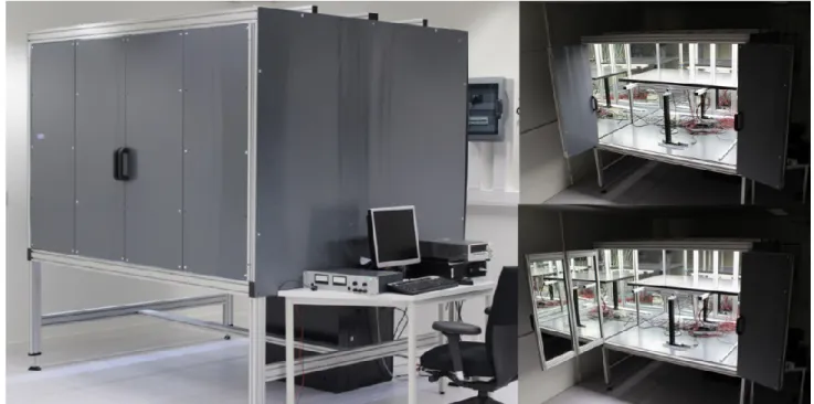
For easy access to the test chamber, two sets of door were installed. The front and main door (Figure 17) allows full access to the front of the setup which allows assembly and removal of the PV modules. This door is composed of four foldable parts to make a smaller opening radius thus occupying less space when opened. The back door (smaller than the front door, shown in Figure 18) is a support door for the handling of the large PV modules. This door is smaller and composed of 2 parts.
The test area is fixed on to two lifting columns with a range of 500 mm, which means that the test area can be positioned between 100 mm and 600 mm, as measured from the light source. The connection between the test area and the columns are hinged to allow different incident angles. The test area can tilt, from a horizontal position, an angle of -40o to 40o (this is the maximum angle permitted when the horizontal test area is at 600mm from the light source.). This guarantees flexibility to the experiments to come.
The aluminium frame provides mechanical support for the mirrors but, used to increase the irradiance and its uniformity, but reduces the effective size of the mirror area and its effect on the irradiance (this effect is described in detail in section 3.6). External panels were mounted to provide mechanical protection for the mirrors and for safety reasons. They are made from PVC which is light weight, cheap and resistant to impact. The roof of the illumination setup is comprised of aluminium sheets were the LED lamps are fixed. Aluminium was chosen because it is lightweight, easy machined and has high heat conductivity, allowing the easy removal of excess heat from the inside of the chamber. This enables the LED to maintain working temperature conditions (~50 oC).
4 CAD – Computer Aided Design
Figure 17 – Front side of the dynamic illumination setup
Figure 18 – Rear side of the dynamic illumination setup
3.3 Illumination
The proposed illumination setup is not to operate as a solar simulator, in the sense that its main objective is not to simulate the sun’s spectrum. The purpose is to create dynamic irradiance patterns characterizations of smart PV modules topologies.
The illumination setup was made to recreate Belgium’s average irradiance conditions. Belgium climate is favourable to cloud formation, which means highly variable irradiance and shading patterns on the ground. The dynamic illumination setup is able to recreate this in a simplified manner with a combination of several LED lamps and the capability of change their brightness. Also, several geometric shapes can be put on top of the PV module to simulate shadows casted from surrounding object.
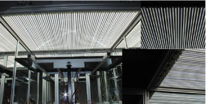
The illumination source is based on LED5 technologies. The setup has 66 T8 LED lamps (Figure 19) powered by LED drivers (Figure 21). The drivers have a PWM6 dimming function which allows to increase or decrease the brightness of the LEDs. The PWM signal is modulated by an Arduino Mega 2560 Rev.3 prototyping board (four board in total and each controls 10 LED drivers). A custom made software to set the duty cycle that regulates the brightness of the LEDs. Standard mirrors (with aluminium coating) are used to improve irradiance uniformity and intensity on the test area. Figure 20 shows the schematic of the lamps, power supply and control systems.
Figure 19 – LED lamps disposition inside to illumination setup
5Light emitting diodes (LED) are light sources in which light is produced by phenomenon of luminescence. An LED is made from a semiconductor known as PN junction. The PN junction on an LED is connected in a forward bias that allows current to flow in one direction. When the electrons are flowing and it comes across a hole the electron in going to shift from the conductive band to the valence band (from higher energy to lower energy status). This transition releases energy in form of heat but mostly in the form of photons. Therefore the LED emits radiation with a certain wavelength depending on the bang gap of the materials that it’s made off.
6 Pulse-width modulation, or PWM for short, uses a rectangular pulse wave whose width is modulated resulting in variation
of the average value of the wave form. This technique uses a digital control (switching on and off) to create the square wave. This simulates a voltages between on and off (0 V and 5 V for the Arduino). With LEDs this results in a chance in brightness, depending on the time that the signal is at 5V or the how long is the duty cycle (example: if the duty cycle is equal to 0% then the LED are off and if the duty cycle is 100% the lamps are at full power).
Figure 21 – Electrical Box with LED drivers
3.4 Light Source
Commercially available standard LED lamps (with SMD 2835 LEDs) were used as illumination source. Each lamp has a rated power of 22 W and a luminous flux of 2150 lm. The luminous efficiency of the lamps is 100 W/lm and it has 120o view angle. The emitted light is between my 400 nm and 800 nm (Figure 22). Each lamp is install side by side (spaced 3 cm from centre to centre) on the roof of the setup (Figure 19).
Figure 22 – SMD 2835 LED spectrum irradiance measured by a spectrometer at a distance of 10mm. Comparison with the AM0 and AM1.5 spectrum irradiance.
To power the lamps, LED driver were used; each driver was connected to 2 lamps in parallel (33 LED driver in total). The LED drivers operate (typically) at 230 VAC and 0.3 A, at 42 VDC (without load) and 0.96 A, in a constant current operation mode. It has a power factor 0.95 and an efficiency of 88.5%. In operation with 2 LED lamps, the driver’s supply 36.6 VDC and 0.9 A (0.45 A per lamp). The power on the DC side for all the lamps is 1.03 kW that translates to an energy consumption of 1.2 kW on the AC side (230 V and 5.1 A RMS). The setup has a separate circuit for dimming the light source.
Inside the lamps there are 180 LEDs (model SMD2835) spaced 8 mm apart, soldered to a PCB7. The configuration is shown in Figure 23. The LED have a maximum operating voltage of 5 V and can handle a current of 60 mA. In the described configuration each LED is operated at 3.66 V and 25 mA. The difference of maximum values to the values supplied is due to the close proximity of the lamps and the lack of forced cooling. This avoids the temperature to rise more than 50 oC (operating temperature of the lamps).
Figure 23 – Schematic of the electrical circuit of the LED lamps
Mirrors were added to further increase the irradiance and uniformity on the test area. A spectrum analysis was conducted to verify the reflectivity of a standard mirror sample. The results are shown in Figure 24. For the relevant spectral range (the one emitted by the LEDs) the average reflectivity is 90.46%. The results of the irradiance and uniformity are presented in session 3.6.
Figure 24 – Spectrum reflectivity measurement for a standard mirror
7 PCB – Printed Circuit Board
3.5 Light source control
The LED drivers have an integrated dimming function that operates at 10 VDC is controlled using a PWM signal. To generate this signal and Arduino8 Mega 2560 Rev3 prototyping board is used. This board generated a 5VDC PWM signal at a frequency of 1kHz9.
Four Arduino boards are used to control the PWM of all the LED drivers (each of them controls 10 LED drivers, except the last that only controls three). One of the Arduino’s was define has Master, which generates the PWM values and transmits it to the remaining slave boards. Each Arduino has a shield10 with 10 MOSFETs (BS170) which act has a bridge between the 10 V dimming circuit of the drivers and the Arduino’s 5 V PWM signal. A 12 VDC power supply is used and regulated to 10 VDC to power the shileds. The communication among boards is made using I2C11. Figure 25 shows the schematic of this circuit.
The code and the procedure to operate the software are described in Attachment 1. The code used to control he Arduino master and slave boards can be found in attachment 2.
8 Arduino is a series of single-board microcontrollers. This hardware is open source. To extend the capabilities of the Arduino shields are used (placed on top), that can be custom made depending on the users’ needs. The board used in the solar simulator is an Arduino Mega 2560 Rev3. It has 54 digital input/output pins, which 15 output PWM signal, 16 analog pins, serial and I2C communication capability. To program this board the Arduino software is used which is based one C++ language.
9 The frequency is made possible by using a PWM.h library in the code to manipulate the clock speed of the Arduino. 10 Small PCB mounted on the Arduino board
11I2C is a communication protocol that allows multiple slave devices to communicate with the master device. This protocol sends an 8 bit signal from the master to the slaves, and vice versa, that contains the address that identifies the slave and the commands.
Figure 25 – Schematic drawing of the electrical circuit of the Arduino’s shield to convert a 5V PWM to a 10V PWM signal
To make it easy to create illumination patterns a script with a GUI12 was made using PowerShell13. This software serves as the input to the Arduinos, which generate de PWM signal. The communication between the script and the Arduinos is made via a serial communication protocol (or USB)14. Each group of LEDs can be controlled individually in the GUI by attributing a value between 0 % and 100 %, the user can regulate the brightness of the LEDs.
There are two type of simulation: ‒ Steady-State Simulation; ‒ Dynamic Simulation;
With the steady-state simulation it is possible to create stationary patterns. By adjusting the brightness of individual groups, or of all groups, a patterns is created. Using the dynamic simulation the software allows the pattern to move to simulate simplified shadow and uneven irradiance intensities over the test plane.
Figure 26 – GUI to control the lamps brightness
The procedure to operate the GUI is presented in Attachment 1 – Code for the Graphic User interface to control the dynamic illumination Setup.
3.6 Irradiance and irradiance uniformity
A spectrometer was used to measure the irradiance, in order to verify the irradiance uniformity and intensity in the illumination setup. A slightly bigger area then the 1x1.6 m2 (test area) was define for the measurements.
12 GUI - Graphic User Interface
13PowerShell is a task automation and configuration management framework form Microsoft, consisting of a command-line shell and associated scripting language built on the .Net Framework.
14 Serial communication is the process of sending data one bit at a time, sequentially, over a communication channel or computer bus.
This area is 1.5x1.8 m2 and was divided in 72 segments. The irradiance was measured in every of the 72 segments at 600 mm to 100 mm (with steps of 100 mm) from the light source.
To quantify the irradiance uniformity on the test area an expression taken from the IEC60904-9 was used. This non-uniformity index (Ω) make a relationship between the maximum (Emax) and the minimum irradiance (Emin)
and gives the percentage of non-uniformity. Ω
=
𝐸𝑚𝑎𝑥−𝐸𝑚𝑖𝑛𝐸𝑚𝑎𝑥+𝐸𝑚𝑖𝑛
× 100
(12)An analysis of the measurement results provides more detail about the irradiance distribution on the test area. This result is shown in Figure 27. At 100 mm from the light source the irradiance distribution suffers greatly with the influence of the individual LED (the highlighted area at 100 mm in Figure 27 shows this effect) and the effect of the mirrors is almost non-existent. Thus the non-uniformity index is the highest for all of the heights, as shown in Table 3.
For 200 mm up to 600 mm from the light source, the mirrors have more effect on the uniformity. Also, the effect of single LEDs is neutralized due to the distance. On the other hand the effect of the aluminium frame starts to have effect on the measurement. At this height it is possible to see a shift of the maximum irradiance value to the back side of the setup. This is consequence of the aluminium beams (on the back side of the setup there are less aluminium beams and more mirror surface compared to the front side) reducing the reflectivity effect of the mirrors.
According to the IEC60904-9 standard, the illumination setup can be labelled as class C for non-uniformity, for all height except at 100mm from the light source. This was chosen as a reference point in terms of irradiance uniformity over the test area for comparison with commercial solar simulators. The other classifications proposed by the standard were not made since it is not relevant for the intended purpose of the setup. Table 3 sums up the results from this measurements and the non-uniformity index.
Table 3 – Minimum, maximum and average irradiance values measured on the test area (1x1.6m2) and the
non-uniformity index for each height
@0,1 m @0,2 m @0,3 m @0,4 m @0,5 m @0,6 m Minimum irradiance [W/m2] 128.55 136.1 125.25 115.67 110.63 108.28
Average irradiance with mirrors [W/m2] 156.01 146.4 139.25 130.02 122.27 120.97
Maximum Irradiance [W/m2] 178.52 157.59 149.08 141.2 132.36 131.03
Figure 27 – Irradiance [W/m2] and uniformity for the test area (1x1.6m2), for different distances from the
light source. The measurements presented in the chart were taken with the lamps at full power and for different height.
3.7 Future development
One of the upgrades foreseen for the setup, and presently under development, is the increase of illumination intensity. To this purpose, the LED drivers are being replaced with power supply that increases the power input to the lamps from 16W to 40W (it will more than triple the irradiance). Also, the electrical system is being redone to handle the increase in power and a cooling system in the lamps is being implemented (so the lamps do not exceed a working temperature of 60oC). Apart from increasing the irradiance this upgrade will increase the spatial resolution since it will allow controlling the brightness of the lamps individually, instead of in pairs. Attachment 3 – Dynamic illumination setup upgrade 1 describes in more detail this upgrade.
Other upgrade that can be performed is the control of temperature and humidity inside the test chamber. This will allow more degrees of freedom in future experiment and increase the controllability on the setup. Also, it will permit more precise results for the energies yield of a smart PV module under different irradiance and environmental condition.
A closer approximation to the solar spectrum and increase the irradiance to 1 sum (or more) would bring the dynamic illumination setup closer to what a commercial solar simulator does. However, it will still provide much more flexibility in terms of testing capability.
4 Conclusion
The work presented in this thesis has focused on the development and evaluation of a dynamic illumination setup that can be used to evaluate the performance of (smart) PV modules. It uses LED technology as its illumination setup (with fully controllable brightness) that provide an average irradiance between 120.97 W/m2 and 156.01W/ m2 (600mm and 100mm from the light source and at full power, respectively). It can create different dynamically varying irradiance patterns (by changing the brightness of groups of LEDs) and intensities, the illumination setup is also able to vary the distance and angle of the PV modules in relation to the illumination source.
The purpose of this setup is to test regular and smart PV modules under non-ideal dynamic conditions, and to determine their performance under different irradiance conditions. Such tests can be with illumination patterns that change in space and time. The irradiance condition that this setup produces corresponds to climate conditions (such as in Belgium) with highly variable irradiance and shading effect (consequence of clouds). But also other dynamic shading patterns due e.g. moving objects or soiling can be tested here.
As this is low-cost tool, several issues that are normal for a solar simulator were traded off, such has the maximum irradiance possible and spectrum match, irradiance uniformity and climate control inside the test chamber (temperature and humidity). In principle, this drawbacks do not affect the main purpose of the illumination setup and can be overcome potentially with future upgrades.
5 References
[1] “IWT-SBO project SmartPV (#110025),” 2011.
[2] T. S. and E. L. J. Kalisch, “Meteorological modeling: Short-term forecasting and nowcasting of solar irradiance,” 2014.
[3] P. Ronan, “Electromagnetic radiation spectrum,” 2007. [Online]. Available: https://commons.wikimedia.org/wiki/File:EM_spectrum.svg.
[4] “Reference Solar Spectral Irradiance: Air Mass 1.5.” [Online]. Available: rredc.nrel.gov/solar/spectra/am1.5/.
[5] “p–n junction.” [Online]. Available: https://en.wikipedia.org/wiki/P%E2%80%93n_junction. [6] I. 60904-9:2007, Photovoltaic devices - Part 9: Solar simulator performance requirements, edition
2.0. 2009.
[7] “Average Daily Solar Irradiance.” [Online]. Available: http://re.jrc.ec.europa.eu/pvgis/apps4/pvest.php#.
[8] “IWT-SBO project SmartPV (#110025),” 2011.
[9] B. (KULeuven/imec) Herteleer, “High frequency outdoor measurements of photovoltaic modules using an innovative measurment set-up,” 2014.
[10] G. V. d. (KULeuven) Broeck, “Substring-level energy-yield assessment of photovoltaic modules subject to partial shading conditions,” 2015.
[11] H. (KULeuven/imec) Goverde, “Energy yield prediction model for PV modules including spatial and temporal effects,” 2015.
[12] “A collection of resources for the photovoltaic educator.” [Online]. Available: http://pveducation.org/. [13] I. 60904-9:2007, Photovoltaic devices - Part 9: Solar simulator performance requirements, edition 2.0. 2009.
[14] P. Ronan, “Electromagnetic radiation spectrum,” 2007. [Online]. Available: https://commons.wikimedia.org/wiki/File:EM_spectrum.svg.
[15] “Photoelectric effect.” [Online]. Available: https://en.wikipedia.org/wiki/Photoelectric_effect. [16] “Solar cell.” [Online]. Available: https://en.wikipedia.org/wiki/Solar_cell.
[17] “Theory of solar cells.” [Online]. Available: https://en.wikipedia.org/wiki/Theory_of_solar_cells. [18] “Semiconductor.” [Online]. Available:
https://en.wikipedia.org/wiki/Semiconductor#Preparation_of_semiconductor_materials.
[19] “Basic Electronics Tutorials for beginners and beyond.” [Online]. Available: http://www.electronics-tutorials.ws/category/diode.
[20] M. Bliss, T. R. Betts, and R. Gottschalg, “Indoor measurement of photovoltaic device characteristics at varying irradiance, temperature and spectrum for energy rating,” Meas. Sci. Technol., vol. 21, no. 11, p. 115701, Nov. 2010.
[21] D. S. Codd, A. Carlson, J. Rees, and A. H. Slocum, “A low cost high flux solar simulator,” Sol. Energy, vol. 84, no. 12, pp. 2202–2212, Dec. 2010.
[22] B. H. Hamadani, K. Chua, J. Roller, M. J. Bennahmias, B. Campbell, H. W. Yoon, and B. Dougherty, “Towards realization of a large-area light-emitting diode-based solar simulator †,” no. November 2011, pp. 779–789, 2013.
[23] S. H. Jang and M. W. Shin, “Fabrication and thermal optimization of LED solar cell simulator,” Curr. Appl. Phys., vol. 10, no. 3, pp. S537–S539, May 2010.
[24] D. Kolberg, F. Schubert, K. Klameth, and D. M. Spinner, “Homogeneity and Lifetime Performance of a Tunable Close Match LED Solar Simulator,” Energy Procedia, vol. 27, pp. 306–311, Jan. 2012.
[25] Q. Meng, Y. Wang, and L. Zhang, “Irradiance characteristics and optimization design of a large-scale solar simulator,” Sol. Energy, vol. 85, no. 9, pp. 1758–1767, Sep. 2011.
[26] M. Stuckelberger, B. Perruche, M. Bonnet-Eymard, Y. Riesen, M. Despeisse, F.-J. Haug, and C. Ballif, “Class AAA LED-Based Solar Simulator for Steady-State Measurements and Light Soaking,” IEEE J. Photovoltaics, vol. 4, no. 5, pp. 1282–1287, Sep. 2014.
Attachment 1 – Code for the Graphic User interface to control the dynamic
illumination Setup
To create the illumination patterns and to set the LED irradiance levels a Graphic User Interface (GUI) was designed. PowerShell15 was used to make a custom-made software to create steady-state or dynamic irradiance patterns.
This software serve as the input to the Arduinos, which generate de PWM signal. The communication between the GUI and the Arduinos is made via a serial communication protocol (or USB). Each group of LEDs can be controlled individually in the GUI. By attributing a value between 0 % and 100 %, the user can regulate the brightness of the LEDs.
There are two type of simulation: ‒ Steady-State Simulation; ‒ Dynamic Simulation;
With the steady-state simulation it is possible to create stationary patterns. By adjusting the brightness of individual groups or of all groups a patterns is created. Using the dynamic simulation the software allows the pattern to move to simulate simplified shadow and uneven irradiance intensities over the test plane.
Figure 28 – GUI for the Dynamic Illumination Control.
Figure 28 note: 1 – Control menu’s; 2 – Status of the Arduino (online or offline); 3 – Lamp groups control area; 4 – Set Brightness (0% to 100%) for all lamps; 5 – Set brightness and lamp off buttons (steady-state simulations); 6 – Set the rate of change for dynamic tests (minimum value is 1 second); 7 – Star and stop buttons for dynamic test; 8 – Set Brightness (0% to 100%) for singles group of lamps; 9 – Clock
15PowerShell is a task automation and configuration management framework form Microsoft, consisting of a command-line shell and associated scripting language built on the .Net Framework.
Procedure to operate the software:
1. Connect the Arduino (Mega 2560) to the PC via a USB cable
2. Check the COM port number of the Arduino by (administrator rights may be needed) 2.1. Pressing the Start button of the desktop environment
2.2. Go to Control Panel 2.3. Click System
2.4. Click Device Manager
2.5. The COM port number in under Collapse Ports (COM & LPT) 3. Run the software “Arduino GUI_Dynamic Illumination Setup”
3.1. Go to Menu and select Arduino
3.2. Choose he Arduino Type (Mega 2560 or Due)
3.3. Choose the COM port number according to the Device Manager
3.4. Software will auto detect if the Arduino is Online
4. Go to Lamp Control and select the type of simulation
4.1. Steady-State simulation
4.2. Dynamic simulation 4.2.1. Left-to-Right 4.2.2. Right-to-Left 5. Create a Pattern
5.1. It is possible to save or load patterns (go to File)16
5.2. Steady-State simulation
5.2.1. Click Set to make the pattern 5.2.2. Click Off to turn off the lamps 5.3. Dynamic simulation
5.3.1. Define the refresh rate 5.3.2. Click Start to start the pattern 5.3.3. Click Stop to stop the pattern 5.3.4. Click Off to turn off the lamps
Attachment 2 – Code for the Arduino’s to control the dynamic illumination setup
The Arduino Mega 2650 is a prototyping board that has 15 PWM pin in which 10 are used to control the array of LED tubes. The pins used have 16 bit timers that allow to use a 1000Hz frequency (using the PWM.h library in the Arduino’s code). Arduino Master CODE: /*
IMEC - Solar Simulator
Code for Master board - Controls LED drivers 1 to 10 Created: 24-04-2015
by Nuno Ruas */
//---libraries---
#include <Wire.h> //include I2C library
#include <PWM.h>//include PWM library to change frequency of PWM pin's //---libraries---
//---Variables---
int freqPin = 1000; //set frequency for PWM pins [Hz] boolean SerialComComplete = false;
const byte pwmPins[] = {12,11,8,7,6,3,2,44,45,46}; //set mostfet pwm pin (of 16 bit timers) - Note: don't use 8 bit timers <=> Timer0 [pin 13 and 4] and Timer2 [pin 9 and 10] NOTE: pin5 doesn,t works with this library (don't know why)
const byte Master=10; // number of PWM pins on the MasterBoard
const byte SlaveOne=20; // number of PWM pins on the MasterBoard plus Slave#1
const byte SlaveTwo=30; // number of PWM pins on the MasterBoard plus Slave#1 plus Slave#2
const byte SlaveThree=33; // number of PWM pins on the MasterBoard plus Slave#1 plus Slave#2 plus Slave#3 int ledBrightness[]={0,0,0,0,0,0,0,0,0,0,0,0,0,0,0,0,0,0,0,0,0,0,0,0,0,0,0,0,0,0,0,0,0}; //define initial LED Brightness from 0 (100%) to 255 (0%) //---Variables--- void setup() { Serial.begin(115200);
Wire.begin(); //join i2c bus - MASTER
InitTimersSafe(); //Initializes all timers except timer 0 is not initialized in order to preserve time keeping functions
for (int x=0;x<Master;x++) { pinMode(pwmPins[x], OUTPUT); SetPinFrequencySafe(pwmPins[x], freqPin); } } void loop() { }
void serialEvent() //function that receives the data from the PC {
while (Serial.available()) {
slave device #1 - all PWM pin }
for (int i=0;i<33;i++) {
ledBrightness[i] = map(Serial.parseInt(),100,0,0,255);
Serial.print(i); Serial.print("-"); Serial.println(ledBrightness[i]); } if (Serial.read() == '\n'); { SerialComComplete = true; } } if (SerialComComplete = true) {
for (int x=0;x<SlaveThree;x++) {
if (x<Master) {
pwmWrite(pwmPins[x],ledBrightness[x]); }
else if (x>=Master && x<SlaveOne) {
transmit(1, x); //transmits to & x<SlaveTwo) {
transmit(2, x); //transmits to slave device #2 - all PWM pin }
else if (x>=SlaveTwo && x<SlaveThree) {
transmit(3, x); //transmits to slave device #3 - all PWM pin }
}
SerialComComplete = false; }
}
void transmit(int slaveNum, int menu) //function that transmits data to the slaves { Wire.beginTransmission(slaveNum); Wire.write(menu); Wire.write(ledBrightness[menu]); Wire.endTransmission(); }
Arduino Slave1 CODE17: /*
IMEC - Solar Simulator
Code for Slave #1 board - Controls LED drivers 11 to 20 Created: 24-04-2015
by Nuno Ruas */
//---libraries---
#include <Wire.h> //include I2C library
#include <PWM.h>//include PWM library to change frequency of PWM pin's //---libraries---
//---Variables---
int freqPin = 1000; //set frequency for PWM pins [Hz]
const byte pwmPins[] = {12,11,8,7,6,3,2,44,45,46}; //set mostfet pwm pin (of 16 bit timers) - Note: don't use 8 bit timers <=> Timer0 [pin 13 and 4] and Timer2 [pin 9 and 10] NOTE: pin5 doesn,t works with this library (don't know why)
byte ledBrightness[] = {0,0,0,0,0,0,0,0,0,0};
const byte numPins=10; //mamenuNumimum number os PWM port on the SlaveBoard //---Variables---
void setup() {
Serial.begin(9600);
Wire.begin(1); // join i2c bus_MASTER TO SLAVE 1
InitTimersSafe(); // Initializes all timers emenuNumcept timer 0 is not initialized in order to preserve time keeping functions
Wire.onReceive(receiveBrightness); //register for (int x=0;x<numPins;x++)
{ pinMode(pwmPins[x], OUTPUT); SetPinFrequencySafe(pwmPins[x], freqPin); } } void loop() {
for (int x=0;x<numPins;x++) {
pwmWrite(pwmPins[x], ledBrightness[x]); }
}
void receiveBrightness (int howMany) {
int menuNum = Wire.read(); switch (menuNum) { case 10: menuNum = menuNum-10; ledBrightness[menuNum]=Wire.read(); break; case 11: menuNum = menuNum-10; ledBrightness[menuNum]=Wire.read(); break; case 12: menuNum = menuNum-10; ledBrightness[menuNum]=Wire.read(); break; case 13: menuNum = menuNum-10; ledBrightness[menuNum]=Wire.read(); break;
case 14: menuNum = menuNum-10; ledBrightness[menuNum]=Wire.read(); break; case 15: menuNum = menuNum-10; ledBrightness[menuNum]=Wire.read(); break; case 16: menuNum = menuNum-10; ledBrightness[menuNum]=Wire.read(); break; case 17: menuNum = menuNum-10; ledBrightness[menuNum]=Wire.read(); break; case 18: menuNum = menuNum-10; ledBrightness[menuNum]=Wire.read(); break; case 19: menuNum = menuNum-10; ledBrightness[menuNum]=Wire.read(); break; } }
Attachment 3 – Dynamic illumination setup upgrade 1
The irradiance from the lamps is low and it is limiting in terms of what experiment can be done. This upgrade will increase the input power of the LED and consequently allow the increase of the irradiance.
Table 4 shows the specification of the current system. Currently, each lamp operates at a 16W due to the fact that the LED drivers don’t supply enough voltage. To be able to increase the irradiance of the lamps it is necessary to supply more power to it.
This upgrade will more than triple the irradiance, increase the special resolution (instead of the lamps being controlled in pair, it is control individually), increase the response time of the lamps (before limited by the drivers to a minimum of 1 second).
To reach the rated power of the lamps will be necessary to supply 40V and 0.5A (without forced cooling). This means that each of 180 led (inside the lamps) is supplied with 4V and 27.7mA. It was determined that the LEDs inside the lamp can operate at double the current, although it will be necessary cooling to dissipate excess heat. With this each lamp will need 40V and 1A (allowing to more than triple the irradiance of the lamps).
Table 4 – Lamp and LED driver specification
Lamp specifications
LED driver specifications
(without cooling) (with cooling) (without load) (without load)
Per lamp Per lamp 2 lamps Per lamp
Voltage [V]
40 40 42 36.6 36.6Current [A]
0.5 1 0.96 0.91 0.455Power [W]
20 40 40 33 16.5To upgrade the setup new power electrical system is needed. The current LED lamps will be maintain, but the LED driver will be replaced. As a replacement a power supply that provides 48 V (adjusted between 42V and 56V) and 10.5A will be installed (7 will be need to power all the lamps). Each power supply will have 10 lamps (mounted in parallel). Individually, every lamp will have an electronic circuit so adjust its brightness.
To control the brightness of the lamps a new electronic scheme will be implemented. Logic level mosfet, capable of handling the new setup, will serve as a link between Arduino. A new shield will be design, where the mosfet’s are going to be soldered so the Arduino’s continue to regulate the PWM (instead of 4, 7 Arduino’s will be used). Figure 29 and Figure 30 shows the PCB designed and electrical schematic, respectively.
To coup with the increase power a cooling system will be installed. This is so the lamps don’t work above 50oC and maintain its life span. The cooling system will use chilled water that will flow through heatsinks (with copper tubing incorporated).
![Figure 2 – EM spectrum of the sun. In green represents the EM spectrum before entering the atmosphere and in blue after entering the atmosphere [4]](https://thumb-eu.123doks.com/thumbv2/123dok_br/19186373.947753/12.892.127.768.121.519/figure-spectrum-represents-spectrum-entering-atmosphere-entering-atmosphere.webp)
![Figure 8 – Representation of a PV Junction [5]](https://thumb-eu.123doks.com/thumbv2/123dok_br/19186373.947753/15.892.218.677.238.523/figure-representation-pv-junction.webp)