1
Seed-Layer Free Zinc Tin Oxide Tailored Nanostructures for
2
Nanoelectronic Applications: E
ffect of Chemical Parameters
3
Ana Rovisco, Rita Branquinho, Jorge Martins, Maria João Oliveira, Daniela Nunes, Elvira Fortunato,
4Rodrigo Martins, and Pedro Barquinha
*
5i3N/CENIMAT, Department of Materials Science, Faculty of Science and Technology, Universidade NOVA de Lisboa and
6 CEMOP/UNINOVA, Campus de Caparica, 2829-516 Caparica, Portugal
7
*
S Supporting Information8 ABSTRACT: Semiconductor nanowires are mostly processed by complex,
9 expensive, and high temperature methods. In this work, with the intent of
10 developing zinc tin oxide nanowires (ZTO NWs) by cost and
low-11 complexity processes, we show a detailed study on the influence of chemical
12 parameters in the hydrothermal synthesis of ZTO nanostructures at
13 temperatures of only 200 °C. Two different zinc precursors, the ratio
14 between zinc and tin precursors, and the concentration of the surfactant agent 15 and of the mineralizer were studied. The type and the crystallinity of the 16 nanostructures were found to be highly dependent on the used precursors and 17 on the concentration of each reagent. Conditions for obtaining different ZTO 18 nanostructures were achieved, namely, Zn2SnO4 nanoparticles and ZnSnO3 19 nanowires with length∼600 nm, with the latter being reported for the first 20 time ever by hydrothermal methods without the use of seed layers. Optical 21 and electrical properties were analyzed, obtaining band gaps of 3.60 and 3.46
22 eV for ZnSnO3 and Zn2SnO4, respectively, and a resistivity of 1.42 kΩ·cm for single ZnSnO3 nanowires, measured using 23 nanomanipulators after localized deposition of Pt electrodes by e-beam assisted gas decomposition. The low-temperature 24 hydrothermal methods explored here proved to be a low-cost, reproducible, and highlyflexible route to obtain multicomponent 25 oxide nanostructures, particularly ZTO NWs. The diversity of the synthesized ZTO structures has potential application in next-26 generation nanoscale devices such asfield effect nanotransistors, nanogenerators, resistive switching memories, gas sensors, and 27 photocatalysis.
28 KEYWORDS: nanostructure, nanowire, Zn2SnO4, ZnSnO3, hydrothermal synthesis, ZTO
29
■
INTRODUCTION30The increasing demand to have smart and multifunctional 31surfaces on all sorts of objects and shapes is pushing flexible 32and transparent electronics to unprecedented performance and 33integration levels.1For this end, it is highly desirable a material 34system offering sustainability in terms of raw materials and 35processes to synthesize its low-dimensional structures, 36combined with a wide range of properties to enable its use 37on transistors, sensing, or even energy-harvesting components. 38Metal oxides are one of the material classes with the highest 39potential to fulfill all these needs. In fact, ZnO-based
40nanostructures have been widely explored over the past
41decade.2,3 ZnO nanowires are a good example of the
42multifunctionality of oxides, enabling for instance nano-43generators to act as gas sensors and biosensors.4,5 Moving 44from single to multicomponent oxides, e.g., from ZnO to zinc 45tin oxide (ZTO), has been one of the current trends, enabling 46one to obtain different properties by adjusting the cationic 47ratio, resulting in a wider range of applications for a given 48material system.6 Concerning sustainability, ZTO also has a 49great advantage over other multicomponent oxides as the well-50established indium−gallium−zinc oxide (IGZO) in thin-film
51
technologies, since it avoids the use of critical raw materials as
52
In and Ga.7
53
ZTO can crystallize through solid-state reaction in the
54
metastable perovskite (orthorhombic or face centered, fcc)8or
55
rhombohedral9 forms (ZnSnO3) and the more stable inverse 56
spinel orthostannate (Zn2SnO4). 10,11
In Figure S1 in 57 Supporting Informationthe crystalline structure of both phases
58
is presented.
59
Zn2SnO4is an n-type semiconductor with mobilities higher 60
than 10−15 cm2V−1s−1and a wide band gap of 3.6 eV being 61
reported in nanostructures.12On the other hand, ZnSnO3has 62
been reported as an excellent piezoelectric material, with a
63
piezoelectric potential along the c-axis of ∼59 μC/cm2, more 64
than 1 order of magnitude higher than that of ZnO (∼5 μC/
65
cm2),13−15
and also as a ferroelectric material.16Its band gap
66
was reported as being 3.9 eV, higher than for Zn2SnO4.17,18 67
These ZTO nanostructures can be synthesized by vapor phase
68
processes as chemical vapor deposition (CVD)19and thermal
Received: May 7, 2018 Accepted: July 20, 2018 Published: July 20, 2018
Article
www.acsanm.org
© XXXX American Chemical Society A DOI:10.1021/acsanm.8b00743
69evaporation,6which present high efficiency. However, these are
70cumbersome and expensive techniques, which demand high
71temperatures (>700°C). Thereby, solution-based methods are 72imperative to decrease complexity, cost, and temperature while 73still enabling good performance of the synthesized nanostruc-74tures. Solution-based hydrothermal methods were already used 75to obtain ZTO nanostructures such as nanoparticles (NPs),20 76nanowires (NWs),21 nanorods,22 octahedrons,23 nanocubes 77(NCs),24,25 and nanoflowers.26 These nanostructures have 78demonstrated interesting properties for numerous applications 79as photocatalysis,27sensors,28−30nanogenerators,31−33resistive 80switching memories,34,35 and solar cells,36 reinforcing the 81multifunctionality of ZTO for next-generation nanoscale 82devices.
83 A proper control of the synthesis process to achieve the 84target structure and shape is crucial. As an example, for gas 85sensing it was already reported that within ZnSnO3structures 86an orthorhombic phase (as the one obtained in this study)
87possesses a much higher sensibility than the fcc. The
88dimension of the obtained structures also plays an important 89role, with higher specific surface areas resulting in improved 90gas sensing performance.37
91 However, two important drawbacks need to be solved:first, 92it is well-known that obtaining a single phase (ZnSnO3 or 93Zn2SnO4) and a single nanostructure shape (e.g., NP or NW) 94by solution processes is quite challenging.38,39This can limit 95the usefulness of ZTO for different applications, as the 96properties are heavily dependent on phase and shape; also, 97low-cost hydrothermal methods, highly desirable from an 98upscaling perspective, always require seed layers to achieve 99ZnSnO3NWs.38,40While the use of a seed layer can enable 100easier fabrication of vertical structures such as gate-all-around 101transistors,41,42 synthesizing ZTO NWs without a seed layer 102also brings multiple advantages: imposes fewer constraints to 103the synthesis conditions to be studied, which is crucial for 104investigating in detail the role of each synthesis parameter in 105controlling phase, shape, and size of the nanostructures;10,43 106allows for fewer processing steps to obtain the nanostructures; 107provides higher degree of freedom to integration by relying on 108a wide variety of available transfer methods to obtain random 109and aligned networks of NWs on any substrate;44finally, the 110nanostructures do not incorporate on their final shape any 111undesired residuals from the seed layers.45
112 In this paper, we present different multicomponent ZTO
113nanostructures produced by a seed-layer-free, one-step hydro-114thermal method, at only 200°C. The chemical and structural 115influence on the solution-based synthesis of the zinc salt, the 116ratio between zinc and tin precursors, the concentration of the 117surfactant agent (H2O:EDA ratio), and the mineralizer 118(NaOH) concentration were studied with the aim of obtaining 119ZTO NWs. We are particularly interested in 1D structures 120given their efficient charge transport, crucial for conceiving 121nanoelectronic devices.46
122 Herein we show a simple hydrothermal method where we
123can control the phase and shape of the nanostructures by 124tuning the chemical parameters of the synthesis. ZnSnO3NWs 125were successfully achieved without the support of seed layers 126and using two different zinc precursors.
127
■
RESULTS AND DISCUSSION128 Introduction: Governing Equations To Obtain ZTO
129NWs. In a typical hydrothermal method to achieve ZTO
130nanostructures, the synthesis product is seldom composed by a
131
single crystalline phase. In fact, ZnSnO3NWs, Zn2SnO4NPs, 132
NCs and octahedrons with nanoplates, ZnO NWs, SnO2NPs
133
and mixtures of them are usually obtained (Figure S2).10It is
134
thus imperative to revise the governing equations representing
135
the chemical processes to achieve each of these phases when
136
Zn and Sn precursors are present.
137
The chemical reaction processes for the formation of
138
ZnSnO3 nanostructures can be represented by the following
139 equations:47 + + → + + − Zn2 Sn4 6OH ZnSn(OH)6 → + ZnSn(OH)6 ZnSnO3 3H O2 140
Concerning Zn2SnO4, its formation can be represented as
141 follows:12,43 + + → ↓ + + − Zn2 Sn4 6OH ZnSn(OH)6 + → + − − Zn2 4OH Zn(OH)42 + → ↓ + + − − ZnSn(OH) Zn(OH) Zn SnO 4H O 2OH 6 4 2 2 4 2 142
While these equations provide an ideal scenario to obtain
143
ZnSnO3and Zn2SnO4nanostructures, it has to be taken into 144
account that the modification of the concentration of the
145
precursors and the mineralizer during the reaction can
146
promote the formation of other species/structures. Moreover,
147
both ZTO phases have ZnSn(OH)6as an intermediary phase 148
(Figure S2), which can also appear as an end product for
149
synthesis with short durations and/or low temperatures. Given
150
this, the detection of OH− groups by FTIR spectroscopy is
151
quite useful for inferring about the completeness of the
152
reaction (Figure S3).
153
Regarding the formation of ZnO nanostructures, it is
154
normally associated with a high alkaline concentration,43and
155
it can be represented by
→ ↓ + +
− −
Zn(OH)42 ZnO H O2 2OH
156
where tin species are washed away after reaction.
157
Finally, with respect to the SnO2 nanostructures,43 its
158
formation is favored by a lower alkaline concentration and can
159
be represented by the following equation:
+ ↔ + + + Sn4 3H O2 H SnO2 3 4H → ↓ + H SnO2 3 SnO2 H O2 + → + − H OH H O2 160
Similar to tin species in the case of a highly alkaline
161
environment, the zinc species are washed away after synthesis.
162
While the cationic ratios and chemical parameters
163
mentioned above dictate which nanostructures within the
164
Zn−Sn−O system are obtained, understanding the growth
165
mechanism for each nanostructure would require a detailed
166
analysis of the effect of physical parameters such as time,
167
temperature, and pressure,43,48,49which is currently underway.
168
Influence of the Zn:Sn Molar Ratio. The type of
169
precursor and the ratio between the metallic elements in the
170
synthesis are crucial to define the nanostructures’ shape, size,
171
and crystallinity. Wefirst studied the different ratios between
172
zinc and tin precursors (2:1, 1:1, and 1:2) using two different
173
zinc sources, zinc acetate (ZnAc) and zinc chloride (ZnCl2). DOI:10.1021/acsanm.8b00743 ACS Appl. Nano Mater. XXXX, XXX, XXX−XXX
174For these studies a NaOH molar concentration of 0.240 M and 175a H2O:EDA volume ratio of 7.5:7.5 mL:mL were used, based 176on the synthesis reported by Li et al.,12where Zn2SnO4NWs 177were grown on a stainless steel mesh for dye-sensitized solar 178cells application.
179 Synthesis using ZnAc as the Zn precursor, with a Zn:Sn
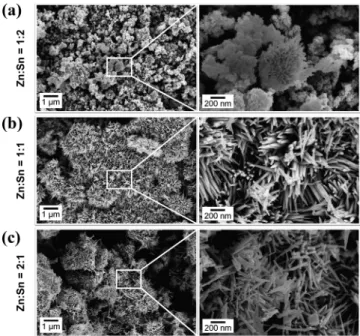
180molar ratio of 1:2, results in inconclusive XRD analysis, 181showing the possible presence of different phases whose f1 182diffraction peaks overlap (Figure 1a): tetragonal phase of SnO2
183(ICDD card 01-077-0452), ZnSnO3orthorhombic perovskite 184phase, and Zn2SnO4inverse spinel phase (ICDD card 00-024-1851470). For the ZnSnO3orthorhombic perovskite phase, peaks 186can be identified by the ICDD card 00-028-1486. It should be 187noted that although this card was removed from the ICDD 188database due to the similarities with a mixture of Zn2SnO4and 189SnO2phases, several reports in the literature48,50−52still refer 190to it. In fact, when we performed peak indexing in different
191ZnSnO3 nanowires samples, an orthorhombic phase was
192always determined. These findings are also supported by
193Raman analysis as will be discussed later.
f2 194 SEM analysis (Figure 2a) supports the argument that some 195ZTO (ZnSnO3 and/or Zn2SnO4) NWs are starting to form. 196This is reinforced by Raman spectroscopy analysis (Figure 197S4a), which shows the predominance of the vibrational band at 198631 cm−1associated with the expansion and contraction of the 199Sn−O bond peak53but also that peaks at 538 and 676 cm−1 200start to appear, corresponding to internal vibrations of the 201oxygen tetrahedron in Zn2SnO4 and to the characteristic
202Raman M−O bonds stretching vibration mode in the MO6
203octahedron of ZnSnO3and/or Zn2SnO4, respectively.43 204 For synthesis with a 1:1 molar ratio of Zn:Sn, ZnSnO3NWs
205are predominantly obtained, as shown by XRD and SEM
206analysis (Figure 1b andFigure 2b). The identification of ortho-207ZnSnO3is not immediately clear: it can be mistaken not only 208with SnO2(as seen before for 1:2 Zn:Sn molar ratio) but also 209with Zn2SnO4inverse spinel-cubic phase (ICDD card 00-024-2101470). EDS analysis on isolated wires shows the ratio Zn:Sn of 2111:1 (Figure S5), supporting the ZnSnO3phase, which was also 212identified by Kovacheva et al.54 on a similar XRD spectra. 213Raman spectroscopy shows that the intensity of the 676 cm−1 214peak (Zn2SnO4or ZnSnO3) increases while the intensity for
215
the 538 cm−1peak (Zn2SnO4) decreases when compared with
216
the sample using 1:2 Zn:Sn ratio. This confirms the
217
predominance of the ZnSnO3phase for the ratio 1:1. (Figure 218
S4a). While SnO2 NPs could not be confirmed by SEM
219
analysis, deeper investigation using SEM and EDS revealed a
220
plausible explanation for the SnO2peak:Figure S5shows that 221
within the same sample some structures comprising
agglom-222
erated NWs could be found. Such structures were reported by
223
Mao et al.55 and have been described as ZnO-doped SnO2.
224
This can be explained by the higher solubility of chlorides in
225
solvents based on ethylenediamine when compared to acetates:
226
the prior dissolution of tin chloride would lead initially to the
227
formation of SnO2nanostructures, which could then be doped
228
by the Zn present in the solution, which falls in line with the
229
Zn and Sn distribution measured by EDS as seen inFigure S6 230
(see alsoFigure S7).
231
XRD data obtained for the synthesis with Zn:Sn molar ratio
232
of 2:1 are similar to the data of 1:1 condition (Figure 1b),
233
suggesting the presence of ZnSnO3perovskite phase. However,
234
SEM inFigure 2c readily shows that besides the ZnSnO3NWs 235
some other structures are present. A more detailed analysis
236
reveals a mixture of ZnSnO3 and Zn2SnO4 octahedrons and 237
NWs, microtubes comprising agglomerates of ZnSnO3 NWs
238
and ZnO nanoplatelets (Figure S8 and Figure S9). Raman
239
spectroscopy data support these results, showing the
240
predominance of the 676 cm−1peak associated with ZnSnO3 241
and/or Zn2SnO4over the 631 cm−1peak from SnO2but also
242
the presence of the 538 cm−1peak corresponding to Zn2SnO4. 243
Furthermore, a small peak at 574 cm−1 is detected for this
244
synthesis condition, attributed to a vibrational mode of ZnO,56
245
concomitant with the SEM analysis.
246
It can be concluded that for the ZnAc precursor a 1:1 Zn:Sn
247
molar ratio is the one allowing us to obtain ZnSnO3 NWs
248
without a large fraction of other Zn- and/or Sn-based
249
nanostructures. As such, this ratio was chosen for the following
250
studies. It should be noted that Li et al. reported Zn2SnO4 251
NWs following a similar synthesis but using a stainless steel
252
mesh as seed, favoring the growth of ZTO nanostructures
253
similar to the cubic structure of the seed.12 Figure 1.XRD patterns for three different Zn:Sn molar ratios (1:2,
1:1, and 2:1) using (a) ZnAc precursor and (b) ZnCl2 precursor. Identification is following ICDD cards 028-1486 (deleted), 00-024-1470, and 01-077-0452 (Figure S2).
Figure 2. SEM micrographs of nanostructures obtained with ZnAc precursor and Zn:Sn molar ratios of (a) 1:2, (b) 1:1, and (c) 2:1.
DOI:10.1021/acsanm.8b00743 ACS Appl. Nano Mater. XXXX, XXX, XXX−XXX
254 The same study was performed using ZnCl2 as zinc 255precursor, with the different Zn:Sn molar ratios of 1:1, 1:2, 2562:1. Using a Zn:Sn molar ratio of 1:2, similar XRD data are 257obtained when compared to the ZnAc precursor, suggesting 258that a tetragonal phase of SnO2and/or a ZnSnO3perovskite 259phase exists (Figure 1b). SEM analysis reveals that both SnO2 260NPs and ZTO (ZnSnO3and/or Zn2SnO4) NWs are obtained f3 261but now with more relevance to the latter (Figure 3a). Raman 262spectroscopy data confirm this, exhibiting a more intense peak 263for ZnSnO3and/or Zn2SnO4(676 cm−1) than for SnO2(636 264cm−1), as seen inFigure S4b.
265 For a solution with Zn:Sn molar ratio of 1:1, the XRD
266spectra show mainly the phase Zn2SnO4, as depicted inFigure 2671b, with some small peaks attributed to ZnSnO3 and SnO2.
268
SEM images show several types of nanostructures: while
269
ZnSnO3 NWs are clearly observed (Figure 3b), a more
270
detailed inspection also reveals a large amount of Zn2SnO4 271
NCs (Figure S10). For the Zn:Sn molar ratio of 2:1 mostly
272
ZnSnO3 NWs are obtained (Figure 3c). Still, a few ZnO
273
columnar nanoplatelets with hexagonal phase (ICDD card
00-274
036-1451) are also shown in Figure S11c. These trends are
275
confirmed by the Raman analysis (Figure S4b), analyzing the
276
evolution of peaks at 538 cm−1 (Zn2SnO4), 676 cm−1
277
(Zn2SnO4 and/or ZnSnO3), and 631 cm−1 (SnO2). Similar
278
structures were already reported by Tian et al.57 for the
279
synthesis of ZnO nanostructures. Figure S11a shows an
280
example of ZnSnO3 NW agglomerates obtained in this
281
condition, which is shown by EDS to have a 1:1 Zn:Sn ratio
282
(Figure S12). Curiously, by looking at the hexagonal form in
283
the middle, we can suggest that the ZTO NWs are grown from
284
an initial hexagonal ZnO microtube/wire. The initial formation
285
of the ZnO NWs can be attributed to the higher solubility of
286
ZnCl2 when compared to SnCl4·5H2O, 55
contributing to the
287
faster formation of these structures relative to the ZnSnO3
288
NWs, which is an issue when trying to obtain single phase
289
ZTO nanostructures. However, according to Miyauchi et al.,
290
these ZnO NWs can be removed with an acid solution of
291
HNO3, 17
allowing us to achieve only ZnSnO3 NWs in the
292
sample. As such, the Zn:Sn ratio of 2:1 was the selected
293
condition for the following studies with the ZnCl2precursor,
294
allowing us to obtain ZnSnO3NWs with an average length of 295
605 nm and a diameter of around 65 nm.
296
For both zinc precursors, for the Zn:Sn molar ratio of 1:2,
297
SnO2 NPs are predominantly obtained, which can be
298
attributed to the higher concentration of tin precursor in the
299
solution. Even so, the initial growth of ZnSnO3NWs is already 300
observed. When the molar ratio is 1:1, the results differ for the
301
two precursors. For ZnAc this was shown to be the best ratio
302
in terms of promoting the growth of a single phase of ZnSnO3
303
NWs. On the other hand, for ZnCl2, this ratio leads to a
304
mixture of Zn2SnO4NCs (predominant) and ZnSnO3 NWs. 305
As for the 2:1 molar ratio of Zn:Sn, it is the condition that
306
promotes better results when using ZnCl2, resulting in ZnSnO3
Figure 3.SEM micrographs of nanostructures obtained with ZnCl2 precursor and Zn:Sn molar ratios of (a) 1:2, (b) 1:1, and (c) 2:1.
Figure 4.XRD patterns when using (a) ZnAc precursor (with 1:1 Zn:Sn ratio) and (b) ZnCl2precursor (with 2:1 Zn:Sn ratio) for different H2O:EDA volume ratios. Identification is following ICDD cards 00-028-1486 (deleted), 00-011-0274, 00-024-1470, 01-077-0452, and 00-06-1451 (Figure S2).
DOI:10.1021/acsanm.8b00743 ACS Appl. Nano Mater. XXXX, XXX, XXX−XXX
307NWs (although mixed with ZnO NWs), while for ZnAc a 308higher mixture of phases, with predominance of Zn2SnO4NCs, 309is achieved.
310 In summary, whichever the ratios, using ZnAc promotes the 311presence of SnO2while using ZnCl2results in higher amounts 312of ZnO. This can be explained by the different precursors’ 313solubility: while SnCl4·5H2O is more soluble than ZnAc, 314promoting a faster growth of tin-based structures, ZnCl2 is 315more soluble than tin chloride, promoting a preferential
316growth of zinc-based structures. Table S1 presents the
317nanostructures sizes for the different conditions of both zinc 318precursors, obtained through the SEM images and using the 319software ImageJ. In general, it is possible to observe that the 320nanostructures produced using ZnCl2 as zinc precursor have 321longer sizes than the nanostructures produced using ZnAc.
322 Influence of the Surfactant Concentration. Oriented
323growth and morphological control of nanostructures are highly 324dependent on surfactant use.43This section presents the study 325of the influence of the H2O:EDA volume ratio for the two 326selected conditions from the previous study: Zn:Sn = 1:1 327molar ratio using the ZnAc precursor and Zn:Sn = 2:1 molar 328ratio using the ZnCl2precursor. The H2O:EDA volume ratios 329used were 15:0, 9:6, 8:7, 7.5:7.5, 8:7, 9:6, and 15:0 mL:mL. 330For all conditions the mineralizer’s (NaOH) concentration was 331kept as 0.240 M.
332 For the ZnAc precursor and using only H2O as a solvent a
333mixture of ZnSnO3 NWs and Zn2SnO4 nanoplates and
f4 334octahedrons comprising nanoplates is obtained (Figure 4a f5 335and Figure 5a), with Zn2SnO4being the predominant phase. 336These types of octahedron structures were already reported by 337Ji et al.23With increasing of EDA up to 7.5:7.5, there is a trend
338
for Zn2SnO4NPs to disappear while ZnSnO3NWs dimensions 339
get larger. SnO2 NPs initially appear as isolated structures 340
moving to SnO2-filled ZnSnO3 NWs as EDA volume is
341
increased (Figure 4a, Figure 5, and Figure S13a). For 7:8
342
volume ratio, there is an increase in the presence of ZnO NWs
343
and ZnSnO3NPs with face centered cubic structure (Figure 4a
344
andFigure 5i,j), due to the higher amount of EDA. Note that
345
ZnSnO3face centered cubic structure and ZnSn(OH)6exhibit
346
coincident Raman peak (603 cm−1)49and XRD peaks (Figures 347 S13 and S2, respectively). Still, for this synthesis condition it is
348
verified by FTIR analysis that no OH− groups are present 349
(Figure S14), confirming the ZnSnO3identification. The ratio 350
6:9 produces mainly ZnO NWs and only a few ZnSnO3NPs as 351
shown by SEM and XRD (Figure 5m and Figure 4a,
352
respectively). When no H2O is used as solvent (0:15), mostly 353
SnO2 NPs and ZnO NWs are obtained, with some ZnSnO3
354
NPs being also present (Figure 4a and Figure 5o). These
355
results are confirmed by Raman spectroscopy (Figure S13a)
356
and can be explained by the significantly higher solubility of
357
SnCl4·5H2O in EDA compared to ZnAc, inducing a faster and 358
preferential growth of SnO2NPs and the later growth of ZnO 359
NWs. Still, probably due to the long duration of the synthesis,
360
some ZnSnO3 NPs are grown, since as previously discussed
361
ZTO nanostructures can originate from SnO2nanostructures.
362
For ZnCl2 as precursor and when using only water as a 363
solvent (15:0 H2O:EDA), Zn2SnO4NPs with octahedral shape 364
are obtained (Figure 5b). The XRD spectra (Figure 4b) show
365
a pure cubic-spinel-type phase for these nanostructures. This is
366
the most stable phase and shape for zinc tin oxide in the
367
absence of EDA, in line with the literature even for other
368
conditions of hydrothermal synthesis.23,58,59With the addition Figure 5.SEM micrographs of the nanostructures obtained by synthesis using ZnAc/ZnCl2as precursors, respectively, with the different H2O:EDA volume ratios of (a, b) 15:0, (c, d) 9:6, (e, f) 8:7, (g, h) 7.5:7.5, (i−l) 7:8, (m, n) 6:9, and (o, p) 0:15.
DOI:10.1021/acsanm.8b00743 ACS Appl. Nano Mater. XXXX, XXX, XXX−XXX
369of EDA, for a H2O:EDA ratio 9:6, Zn2SnO4 nanostructures 370with a different shape than the octahedral and some ZnSnO3
371NWs are obtained, as seen by SEM (Figure 5d). By XRD
372(Figure 4b), it can be verified the mixture of ZnSnO3 and 373Zn2SnO4 phases, with Zn2SnO4 still being predominant. By 374increase of EDA’s concentrations (8:7, 7.5:7.5, and 7:8), the 375size of ZnSnO3 NWs is increased and this phase becomes 376predominant. As Figure 5f shows, for the 8:7 ratio, only
377ZnSnO3 NWs are grown, but they present a large size
378distribution. For the 7.5:7.5 ratio, ZnSnO3and large wires of 379ZnO are obtained, as it was already discussed in section 380Introduction: Governing Equations To Obtain ZTO NWs. For 381the 7:8 ratio the ZnSnO3 NWs are highly agglomerated, as 382shown inFigure 5l. These structures are similar to the obtained 383for ZnAc (7.5:7.5, Zn:Sn = 1:1), as described by Mao et al.55 384The H2O:EDA ratio of 6:9 gives miscellaneous results, as 385Figure 5n andFigure S15show, with a mixture of several types 386of structures being obtained. It is possible to observe Zn2SnO4 387NCs and octahedrons comprising nanoplates, ZnSnO3 NWs, 388SnO2 NPs, and also ZnO columnar nanoplatelets agglomer-389ates, with all of these phases being identified by XRD (Figure 3904b). By use of only EDA (0:15), ZnSnO3NPs and ZnO NWs
391are formed (Figure 5p). The strong ZnO peaks in XRD
392(Figure 4b) appear due to the large size of ZnO NWs when 393comparing with the ZnSnO3 NPs. Overall, the XRD (Figure 3944b) shows that for higher EDA’s concentration, the formation
395
of ZnO becomes preferential over ZTO, which is in agreement
396
with the SEM/EDS and Raman (Figure S13b) analysis. This
397
preferential formation of ZnO nanostructures for the higher
398
EDA conditions can be explained by the strong coordination
399
ability between the ZnCl2and EDA molecules.60,61
400
FTIR analysis helps us to understand and to explain the
401
results for the synthesis where EDA has a higher concentration
402
than H2O. Figure S14a shows that when using ZnAc as zinc
403
precursor, for the conditions with H2O:EDA ratios of 7:8, 6:9, 404
and 0:15, precursor or solvent residuals are still present in the
405
final product, due to the low solubility of ZnAc in EDA. In
406
comparison, for the synthesis using ZnCl2, residuals are
407
observed when only EDA is used as a solvent (Figure
408 S14.b), which can be attributed to the higher solubility of
409
ZnCl2 in EDA, compared to that of ZnAc. For all the other 410
conditions no precursor peaks can be traced by FTIR analysis.
411 Table S2 summarizes the type of nanostructures obtained
412
for the different conditions and their respective dimensions.
413
The trend verified in the previous study regarding the longer
414
sizes of nanostructures synthesized using ZnCl2as compared to
415
ZnAc is again observed here. It is also reinforced the higher
416
presence of Sn-based structures in the synthesis using ZnAc,
417
and a predominance of Zn-based structures in the synthesis
418
using ZnCl2. The addition of EDA favors the formation of
419
ZnSnO3 NWs over the more energetically stable Zn2SnO4 420
NPs, which we attribute to the pH increase, as reported by Figure 6.XRD pattern of the nanostructures obtained for different NaOH concentrations, using (a) ZnAc and (b) ZnCl2as zinc precursors. Identification is following ICDD cards 00-028-1486 (deleted), 00-011-0274, 00-024-1470, 01-077-0452, and 00-036-1451 (Figure S2).
Figure 7.SEM micrographs of the nanostructures obtained by synthesis using different NaOH concentrations.
DOI:10.1021/acsanm.8b00743 ACS Appl. Nano Mater. XXXX, XXX, XXX−XXX
421Miyauchi et al.17Up to a certain EDA concentration the length 422and diameter of these NWs are increased. For both precursors, 423an optimal H2O:EDA volume ratio of 7.5:7.5 was determined 424for the formation of ZnSnO3NWs. As the EDA concentration 425is increased beyond this point, ZnO nanostructures start to be 426dominant, even for the ZnAc precursor. This suggests that the
427predominant factor defining the type of nanostructure
428obtained in an environment with a high EDA concentration 429starts to be the pH value, as will be discussed in more detail in 430the next section. Thus, despite the relevance of EDA to achieve 431the desired ZTO NWs, the presence of the water is imperative 432to the formation of these nanostructures, not only to ensure 433the complete dissolution of the precursors but also to balance 434the pH in solution.
435 Influence of NaOH Concentration. NaOH plays an
436important role in the growth of the nanostructures, acting as a 437mineralizer agent, having a direct influence on the definition of 438the crystalline phase that is produced.
439 On the basis of the previous studies presented in this
440manuscript, the synthesis conditions for this study were set as 441Zn:Sn = 1:1 ratio when using the ZnAc precursor, Zn:Sn = 2:1 442ratio with the ZnCl2precursor, keeping a H2O:EDA ratio of 4437.5:7.5 in both conditions. Concentrations of NaOH of 0.100 444M, 0.175 M, 0.240 M, and 0.350 M were used to understand 445the influence of the mineralizer on the synthesis. The results 446for both zinc precursors presented the same trend, being 447discussed here simultaneously. The poorer concentration of 448NaOH (0.100 M) synthesis results in SnO2 NPs, whichever f6f7 449precursor is used, as seen inFigures 6 and7. Lehnen et al.22 450explained this behavior as an effect of the fast hydrolysis of 451Sn4+ cations, leading to the preferential formation of SnO2. 452With the increasing of the NaOH concentration to 0.175 M, 453SnO2 NPs are still obtained but Zn2SnO4 NPs are now
454predominant. Still, SnO2 is more evident for the ZnAc
455precursor, as shown in the XRD spectra (Figure 6a), which 456would be expected based on the higher solubility of SnCl4· 4575H2O compared to ZnAc. Increasing the NaOH concentration 458to 0.240 M, the Zn2SnO4 phase is no longer present and
459ZnSnO3 NWs are now produced, both in dispersed and in
460agglomerate shapes, as well as some ZnO NWs as already
461discussed in the section Influence of the Zn:Sn Molar Ratio. 462Finally, for the NaOH concentration of 0.350 M, only ZnO 463NWs are obtained when using ZnCl2, while when using ZnAc
464both ZnO NWs and ZnSnO3NPs (ICDD card 00-011-0274)
465are observed. This trend of preferential growth of ZnO in
466
alkaline solutions is well-known, since divalent metal ions do
467
not hydrolyze in acidic environments.62 Even with higher
468
concentrations of NaOH (0.500 M) the resulting structures
469
were verified to be the same as for 0.350 M but with a lower
470
reaction yield. These results are in agreement with the
471
literature, as Lehnen et al.22 showed the same tendency for
472
specific pH values: for pH ≈ 1 SnO2NPs are obtained, pH≈ 473
8.5 yields Zn2SnO4 NPs, and higher pH values yields ZnO 474
mixed with ZnSn(OH)6.
475
Our results show a similar trend; i.e., lower pH leads to
476
SnO2structures and higher pH favors ZnO ones, even if the 477
starting pH (without adding NaOH) is already 12. As such,
478
this trend is not dependent on the pH value itself but in the
479
variation of the NaOH concentration for a specific synthesis.
480 Table S3 summarizes all these findings, showing that low
481
mineralizer concentrations favor the growth of tin oxide
482
structures over zinc oxide ones, with the trend being reversed
483
as the NaOH concentration increases. Having in mind the
484
specific goal of obtaining ZTO NWs, the optimum mineralizer
485
concentration is around 0.240 M.
486
As seen in the previous sections, data inFigure 7andTable 487 S3 reinforce the trend of obtaining nanostructures with larger
488
dimensions using ZnCl2precursor instead of ZnAc, given the
489
higher solubility of ZnCl2.
490
Reproducibility. For a comparison of the precursors in
491
terms of reproducibility, synthesis with the selected conditions
492
(Zn:Sn molar ratio of 1:1 for ZnAc and 2:1 for ZnCl2,
493
H2O:EDA volume ratio of 7.5:7.5 and 0.240 M of NaOH) was
494
repeated at least three times. The results showed a better
495
reproducibility for ZnCl2 than for the ZnAc precursor as
496
discussed next. Figure S16ashows that for three syntheses in
497
the same conditions using ZnCl2 the results are very similar, 498
showing only some differences in the presence of some residual
499
ZnO NWs (confirmed by XRD spectra, in Figure S17b) and
500 f8
some variation in the average size of the ZnSnO3NWs (Figure 501 f8 8b). On the other hand, for the synthesis with ZnAc, three
502
runs already show a quite significant variation on the XRD
503
spectra (Figure S17a), even if all show the predominance of
504
the ZnSnO3 phase (see also SEM images in Figure S16b).
505
Furthermore, the size of the obtained NWs differs substantially
506
for the multiple runs with ZnAc (Figure 8a). As discussed
507
previously, ZnAc has a poor solubility in EDA when compared
508
with ZnCl2and SnCl4·5H2O. This can be one of the factors for 509
the poor reproducibility when using ZnAc as zinc precursor.
510
Moreover, when using ZnCl2, since tin precursor is also a Figure 8. Comparison of the obtained nanostructures dimensions in different repetitions of synthesis using (a) ZnAc and (b) ZnCl2 as zinc precursor, under similar conditions. Average lengths and diameters are given in parentheses.
DOI:10.1021/acsanm.8b00743 ACS Appl. Nano Mater. XXXX, XXX, XXX−XXX
511chloride, the reaction will be less complex: not only is the 512number of chemical species lower, but also as Cl−reacts with 513Na+, the number of possible reactions reduces. Also, in the case 514of ZnAc, the presence of the ionic species H+, O2−, and C+can 515lead to an imbalance in the reaction precluding the formation 516of zinc tin oxide nanostructures.
517 ZnSnO3 Nanowires: Optical and Electrical
Character-518ization. Optical Characterization. To study the optical
519properties of the produced ZnSnO3 NWs, the absorption
f9 520under UV and visible radiation was measured.Figure 9a shows 521the well-known Tauc relation that follows the equation
α νh =A hν−E
( )x ( g)
522whereα is the absorption coefficient, h is the Planck constant, 523ν is the frequency, A is an energy-independent parameter, Egis 524the optical band gap, and x is a coefficient related to the 525electronic transition (x = 2 for allowed direct transition63). 526The Egvalues, inferred by applying the equation to the linear 527region of the plots, are 3.53 and 3.60 eV for the ZnAc and 528ZnCl2 precursors, respectively. For comparison, optical 529properties of pure Zn2SnO4 NPs, produced when using only 530H2O as a solvent (section Influence of the Surfactant 531Concentration), were also evaluated (Figure 9b). A band gap 532of 3.46 eV was achieved, lower than for the ZnSnO3 phase, 533confirming the trends verified by other authors.12,17,18These 534results also confirm the trends typically observed in multi-535component oxides, where the Eg of the resulting structure 536tends to be closer to the Eg of the predominant binary 537compound (ZnO or SnO2).64
538 Still, the Eg values obtained in this work (for both ZnSnO3 539and Zn2SnO4) are slightly lower than the ones reported in 540literature (∼0.15−0.30 eV). This difference can be explained 541by a higher defect density in these nanostructures, resulting in 542absorption close to band edges.65This is a consequence of the 543low temperature of the reported solution-based process (200 544°C) as compared to the >600 °C typically used for physical
545processes. These band gap values suggest a potential
546applicability of these nanostructures for photocatalysis and 547photosensors.66,67
548 Photoluminescence (PL) was also evaluated for these
549samples (Figure 9b). A more evident peak at around 366 nm
550is observed, which can be attributed to ZnO-based
551nanostructures.68By observing the PL spectra, it is clear that 552this peak is more evident in the samples where ZnO-based 553structures were identified (see for instance Table S2), 554corroborating our previous analysis. Small peaks at 427 and 555488 nm can also be identified. The presence of these UV peaks
556
is associated with oxygen vacancies, which are major defects in
557
this type of material,69,70 emissions in this region being
558
common for ZTO nanostructures.71 Other authors also
559
attribute a 428 nm PL peak to SnO contaminations or
560
nanocrystals formed during ZTO synthesis,67which is also a
561
plausible justification for our samples.
562
Electrical Characterization. Electrical measurements on
563
single NWs, although highly desirable for determining its
564
electrical properties, presents itself as a real challenge. In the
565
literature the reported characterizations are related to NWs
566
with lengths of >10 μm. In this work we present electrical
567
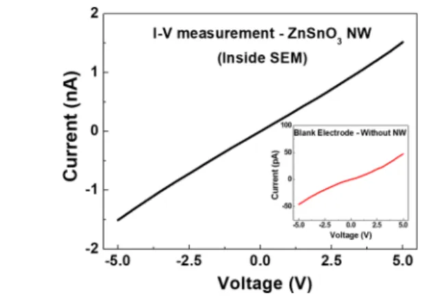
characterization of a single NW with length below 1μm. The
568
data discussed below are for a single NW with length and
569
diameter of 769 and 63 nm, respectively, produced using
570
ZnCl2 precursor, with a Zn:Sn molar ratio of 2:1, H2O:EDA 571
volume ratio of 7.5:7.5 mL, and 0.240 M of NaOH. This
572
condition was selected based on the fact that it is the one
573
enabling higher reproducibility and a larger fraction of
574
dispersed ZnSnO3NW as the synthesis product. The electrical
575
measurement was performed inside SEM using
nanomanipu-576 f10f11
lators after in situ deposition of Pt electrodes (Figure 10). The Figure 9.Tauc’s plots (a) and photoluminescence spectra (b) for ZnSnO3NWs using two different zinc precursors ZnAc and ZnCl2and for Zn2SnO4octahedrons, obtained using ZnCl2precursor with only H2O as solvent.
Figure 10.Images of (a) SEM nanomanipulators and (b) the W tips of the nanomanipulators contacting the Pt electrodes during electrical characterization of a single ZTO NW.
DOI:10.1021/acsanm.8b00743 ACS Appl. Nano Mater. XXXX, XXX, XXX−XXX
f11 577obtained data (Figure 11) show linear I−V characteristics, 578following an ohmic behavior. The background current between
579two electrodes deposited in the same configuration and
580distance (but without a NW connecting them) was also
581measured, as shown in the inset ofFigure 11. This background 582current, resulting from a residual deposition of the electrodes 583material over the sample, was taken into account on the 584calculation of the NW resistivity. The significantly lower 585background current level compared to the actual measurement
586performed in the NW reinforces the validity of the
587nanostructure measurement. Considering Ohm’s law and the 588physical dimensions of the NW, a resistivity of 1.42 kΩ·cm was 589obtained, which is significantly higher than the one reported by 590Xue et al. (∼73 Ω·cm)72for ZnSnO3NWs and by Karthik et 591al. (6Ω·cm in vacuum) for Zn2SnO4NWs.67
592 As explained for the optical properties analysis, the higher 593defect density associated with the low-temperature solution-594based process is the most plausible explanation for the higher 595electrical resistivity reported here (Xue et al.72 synthesized 596NWs by thermal evaporation at 990 °C and Karthik et al.67 597synthesized by vapor phase methods at 900°C).
598 We consider that concluding whether the resistivity obtained 599here is too high for our targeted electronic applications would 600require device fabrication, e.g., field-effect transistors, where 601many other challenges need to be addressed, such as contact 602properties or electrostatic coupling between dielectric and 603semiconductor NW. Even if the synthesized ZTO NWs are too 604resistive for a certain application, there is still room for 605improvement, for instance, by passivation of surface-related 606defects by postannealing in different environments and/or by 607coating with encapsulationfilms.73,74
608
■
CONCLUSIONS609ZnSnO3NWs produced by a solution process without the use 610of a seed layer and with temperatures of only 200 °C were 611reported for the first time. To accomplish this, the work 612presented a detailed study on the influence of the different 613chemical parameters on the hydrothermal synthesis of ZTO 614nanostructures. More specifically the role of Zn:Sn ratio, 615surfactant concentration (EDA), and mineralization agent
616(NaOH) concentration for two zinc precursors (ZnAc and
617ZnCl2) was studied. By adjustment of these parameters, the 618potential to achieve ZTO structures with different phases and
619
morphologies was shown. It was found that an intricate
620
interdependence of the different chemical parameters would
621
enable multiple synthesis conditions to result in thefinal goal
622
of obtaining ZTO NWs. Still, it was concluded that ZnCl2
623
allowed for a more stable (with less mixture of phases/
624
structures) and more reproducible reaction than ZnAc, with
625
longer ZnSnO3 NWs being obtained. Hence, the best
626
condition proved to be using ZnCl2as zinc precursor, with a
627
Zn:Sn molar ration of 2:1, H2O:EDA volume ratio of 7.5:7.5 628
mL:mL, and a NaOH concentration of 0.240 M. These
629
ZnSnO3NWs presented lengths and diameters of around 600 630
and 65 nm, respectively. Electrical characterization of a single
631
NW with a length of <1μm was successfully done inside SEM,
632
using Pt electrodes deposited by localized e-beam assisted gas
633
decomposition. Optical and electrical properties were
com-634
parable with those reported for ZTO NWs produced by
635
physical processes, which employ considerably higher
636
fabrication temperatures. As such, low-temperature
hydro-637
thermal methods proved to be a low-cost, reproducible, and
638
highly flexible route to obtain multicomponent oxide
639
nanostructures, particularly ZTO NWs. Moreover optical and
640
electrical properties showed a great potential for applications
641
such as photocatalysis, nanogenerators, nanotransistors, and
642
gas senors/photosensors.
643
■
EXPERIMENTAL SECTION644
Synthesis of Nanostructures. ZTO nanostructures were
645
synthesized via hydrothermal method, using a modified version of
646
the synthesis reported by Li et al.,12without the use of a seed layer (in
647
ref12a stainless steel mesh seed-layer is used).Figure S18ashows the
648
schematic of the synthesis where the precursor concentrations used
649
were 0.020 M SnCl4·5H2O and 0.040 M Zn(CH3COO)2·2H2O. The
650
precursors were separately dissolved in 7.5 mL of Millipore water and
651
were then mixed together. Afterward, 7.5 mL of the surfactant
652
ethylenediamine (EDA) were added, and the mixture was left stirring
653
for 30 min. Finally 0.240 M NaOH was added. The precursors were
654
smashed in a mortar before being added to water to help dissolution.
655
The reagents used were all commercially available: zinc acetate
656
dihydrate 99.0% (Zn(CH3COO)2·2H2O), sodium hydroxide ≥98%
657
(NaOH), and ethylenediamine 99% (EDA) from Sigma-Aldrich,
658
tin(IV) chloride 5-hydrate (SnCl4·5H2O) extra pure from Riedel-de
659
Haën and zinc chloride 98% (ZnCl2) from Merck.
660
To study the influence of the zinc precursor, zinc acetate was
661
replaced by zinc chloride, maintaining the same concentration of zinc
662
in the solution. Different Zn:Sn ratios (molar concentration) were
663
studied, namely, 2:1, 1:1, and 1:2. The ratio between H2O and EDA
664
was varied (H2O:EDA, 15:0, 9:6, 8:7, 7.5:7.5, 7:8, 6:9, 0:15), as well
665
as the concentration of NaOH (0.100 M, 0.175 M, 0.240, and 0.350
666
M). When the solution was ready, it was transferred into a 45 mL
667
Teflon-lined stainless-steel autoclave, filling 80% of the total autoclave
668
volume. The mixture was kept in an electric oven (Thermo Scientific)
669
at 200°C for 24 h, with a heating ramp of 200 °C/h. The autoclave
670
was cooled to ambient temperature naturally. The resultant
671
precipitate, comprising the nanostructures, was centrifuged at 4000
672
rpm and washed several times with deionized water and isopropyl
673
alcohol, alternately. The nanostructures werefinally dried at 60 °C, in
674
vacuum, for 2 h, as schematized inFigure S18b.
675
Characterization of Nanostructures. Structural characterization
676
by X-ray diffraction (XRD) was performed using a PANalytical’s
677
X’Pert PRO MRD diffractometer with Cu Ka radiation. The XRD
678
data were acquired in the 10−90° 2θ range with a step size of 0.033°,
679
using the nanostructures in the form of powder. Fourier transform
680
infrared (FTIR) spectroscopy data were recorded using an attenuated
681
total reflectance (ATR) sampling accessory (Smart iTR) equipped
682
with a single bounce diamond crystal on a Thermo Nicolet 6700
683
spectrometer. The spectra were acquired with a 45° incident angle in
684
the range of 4000−525 cm−1and with a 4 cm−1resolution. Raman Figure 11.I−V curve for a single ZnSnO3NW contacted by two Pt
electrodes, measured inside SEM using nanomanipulators. The inset shows an I−V curve used for background current extraction, taken from a similar sized Pt electrode structure but without any NW connecting.
DOI:10.1021/acsanm.8b00743 ACS Appl. Nano Mater. XXXX, XXX, XXX−XXX
685spectroscopy measurements were carried out in a Renishaw inVia
686Reflex micro-Raman spectrometer equipped with an air-cooled CCD
687detector and a HeNe laser operating at 50 mW of 532 nm laser
688excitation. The spectral resolution of the spectroscopic system is 0.3
689cm−1. The laser beam was focused with a 50× Leica objective lens (N
690Plan EPI) with a numerical aperture of 0.75. An integration time of 2
691scans (10 s each) was used for all measurements to reduce the
692random background noise induced by the detector, without
693significantly increasing the acquisition time. The intensity of the
694incident laser was 50μW. All spectra were obtained in triplicate for
695each sample at room temperature in the 100−1600 nm range. After 696measurements a baseline subtraction was performed in order to
697identify the different vibrational bands. The band gap of the ZTO 698nanostructures was estimated from reflectance spectra recorded in the 699200−800 nm range with a PerkinElmer lambda 950 UV/vis/NIR
700spectrophotometer using the Tauc plot method. The
photo-701luminescence (PL) measurements were performed at room
temper-702ature, using a PerkinElmer LS.55 instrument with a xenon lamp as
703excitation source with an excitation wavelength of 325 nm. The
704morphology and element analysis of the samples were performed
705using scanning electron microscopy (SEM) and energy dispersive X-706ray spectroscopy (EDS) inside a Carl Zeiss AURIGA CrossBeam
707workstation. The electrical characterization of single-NWs using a
708two-point probe structure was also performed inside the Auriga
709system. First, the NWs were dispersed in isopropyl alcohol, yielding a
710low concentration solution, sonicated during 5 min, and werefinally
711drop-casted on a Si/SiO2substrate. After drying, isolated NWs were
712contacted by Pt electrodes, deposited using localized e-beam assisted
713decomposition of a C5H4CH3Pt(CH3)3precursor introduced close to
714the sample surface using a gas injector system. Kleindiek
nano-715manipulators with W tips were then used to access the current− 716voltage characteristics, together with a semiconductor parameter
717analyzer (Agilent 4155 C).
718
■
ASSOCIATED CONTENT 719*
S Supporting Information720The Supporting Information is available free of charge on the 721ACS Publications website at DOI:10.1021/acsanm.8b00743.
722 Figures showing (1) crystal structures, (2) X-ray
723 diffraction pattern, (3) FTIR spectra before and after
724 synthesis, (5−12) SEM/EDS analysis, (4, 13) Raman
725 spectroscopy related to the studies of Zn:Sn molar ratio
726 and of the H2O:EDA volume ratio, respectively, and
727 (14) FTIR spectra regarding the study of the surfactant
728 concentration; Tables S1, S2, and S3 summarizing the
729 obtainable nanostructures and its dimensions for each of
730 the chemical parameters in study (PDF)
731
■
AUTHOR INFORMATION 732Corresponding Author 733*E-mail:[email protected]. 734ORCID 735Ana Rovisco: 0000-0001-6240-3743 736Rita Branquinho: 0000-0001-9771-8366 737Elvira Fortunato: 0000-0002-4202-7047 738Author Contributions739A.R. designed the experiments, fabricated the nanostructures, 740performed the data analysis, and wrote the manuscript. J.M. 741supported the electrical characterization and its analysis and 742also provided support to manuscript preparation. M.J.O. 743performed the Raman characterization. D.G. provided the 744SEM/EDS characterization. P.B. and R.B. supervised the work 745and revised the concept, structure, and content of the different 746versions of the manuscript until its final form. R.M. and E.F.
747
provided the fabrication and characterization facilities and
748
reviewed thefinal versions of the manuscript.
749 Notes
750
The authors declare no competingfinancial interest.
751
■
ACKNOWLEDGMENTS752
This work is funded by FEDER funds through the COMPETE
753
2020 Programme and national funds through FCT
754
Portuguese Foundation for Science and Technology under
755
Project POCI-01-0145-FEDER-007688, Reference UID/
756
CTM/50025, and the Doctoral Grant Research Number
757
SFRH/BD/131836/2017. This work also received funding
758
from the European Community’s H2020 program under Grant
759
Agreement 716510 (ERC-2016-STG TREND), Grant 685758
760
(1D-Neon), and Grant 692373 (BET-EU).
761
■
REFERENCES(1) Roselli, L.; Borges Carvalho, N.; Alimenti, F.; Mezzanotte, P.; 762 763
Orecchini, G.; Virili, M.; Mariotti, C.; Goncalves, R.; Pinho, P. Smart
764
Surfaces: Large Area Electronics Systems for Internet of Things
765
Enabled by Energy Harvesting. Proc. Proc. IEEE 2014, 102, 1723−
766
1746.
(2) Schmidt-Mende, L.; MacManus-Driscoll, J. L. ZnO -767 768
Nanostructures, Defects, and Devices. Mater. Mater. Today 2007,
769
10, 40−48.
(3) Kołodziejczak-Radzimska, A.; Jesionowski, T. Zinc Oxide770 771
From Synthesis to Application: A Review. Materials 2014, 7, 2833−
772
2881.
(4)Zhao, Y.; Lai, X.; Deng, P.; Nie, Y.; Zhang, Y.; Xing, L.; Xue, X.773 774
Pt/ZnO Nanoarray Nanogenerator as Self-Powered Active Gas
775
Sensor with Linear Ethanol Sensing at Room Temperature.
776
Nanotechnology 2014, 25, 115502.
(5)Zhao, Y.; Deng, P.; Nie, Y.; Wang, P.; Zhang, Y.; Xing, L.; Xue,777 778
X. Biomolecule-Adsorption-Dependent Piezoelectric Output of ZnO
779
Nanowire Nanogenerator and Its Application as Self-Powered Active
780
Biosensor. Biosens. Bioelectron. 2014, 57, 269−275.
(6)Pang, C.; Yan, B.; Liao, L.; Liu, B.; Zheng, Z.; Wu, T.; Sun, H.;781 782
Yu, T. Synthesis, Characterization and Opto-Electrical Properties of
783
Ternary Zn2SnO4Nanowires. Nanotechnology 2010, 21, 465706. (7)Mancini, L.; Sala, S.; Recchioni, M.; Benini, L.; Goralczyk, M.; 784
785
Pennington, D. Potential of Life Cycle Assessment for Supporting the
786
Management of Critical Raw Materials. Int. J. Life Cycle Assess. 2015,
787
20, 100−116.
(8) Guo, R.; Guo, Y.; Duan, H.; Li, H.; Liu, H. Synthesis of 788 789
Orthorhombic Perovskite-Type ZnSnO3 Single-Crystal Nanoplates
790
and Their Application in Energy Harvesting. ACS Appl. Mater.
791
Interfaces 2017, 9, 8271−8279.
(9)Wu, J. M.; Chen, C.-Y.; Zhang, Y.; Chen, K.-H.; Yang, Y.; Hu, Y.; 792 793
He, J.-H.; Wang, Z. L. Ultrahigh Sensitive Piezotronic Strain Sensors
794
Based on a ZnSnO3Nanowire/Microwire. ACS Nano 2012, 6, 4369−
795
4374.
(10) Baruah, S.; Dutta, J. Zinc Stannate Nanostructures: Hydro- 796 797
thermal Synthesis. Sci. Technol. Adv. Mater. 2011, 12, 013004.
(11) Sun, S.; Liang, S. Morphological Zinc Stannate: Synthesis, 798 799
Fundamental Properties and Applications. J. Mater. Chem. A 2017, 5,
800
20534−20560.
(12)Li, Z.; Zhou, Y.; Bao, C.; Xue, G.; Zhang, J.; Liu, J.; Yu, T.; Zou, 801 802
Z. Vertically Building Zn2SnO4 Nanowire Arrays on Stainless Steel
803
Mesh toward Fabrication of Large-Area, Flexible Dye-Sensitized Solar
804
Cells. Nanoscale 2012, 4, 3490−3494.
(13)Lo, M.-K.; Lee, S.-Y.; Chang, K.-S. Study of ZnSnO3-Nanowire805 806
Piezophotocatalyst Using Two-Step Hydrothermal Synthesis. J. Phys.
807
Chem. C 2015, 119, 5218−5224.
(14) Inaguma, Y.; Yoshida, M.; Katsumata, T. A Polar Oxide 808 809
ZnSnO3with a LiNbO3-Type Structure. J. Am. Chem. Soc. 2008, 130,
810
6704−6705.
DOI:10.1021/acsanm.8b00743 ACS Appl. Nano Mater. XXXX, XXX, XXX−XXX
(15)
811 Dal Corso, A.; Posternak, M.; Resta, R.; Baldereschi, A. Ab 812Initio Study of Piezoelectricity and Spontaneous Polarization in ZnO. 813Phys. Rev. B: Condens. Matter Mater. Phys. 1994, 50, 10715−10721.
(16)
814 Mao, Y.; Park, T.-J.; Wong, S. S. Synthesis of Classes of Ternary 815Metal Oxide Nanostructures. Chem. Commun. 2005, 5721.
(17)
816 Miyauchi, M.; Liu, Z.; Zhao, Z.-G.; Anandan, S.; Hara, K. 817Single Crystalline Zinc Stannate Nanoparticles for Efficient Photo-818Electrochemical Devices. Chem. Commun. 2010, 46, 1529−1531.
(18)
819 Lei, M.; Sheng, Y.; Wan, L.; Bi, K.; Huang, K.; Jia, R.; Liu, J.; 820Wang, Y. A Novel Self-Catalytic Route to Zinc Stannate Nanowires 821and Cathodoluminescence and Electrical Transport Properties of a
822Single Nanowire. J. Alloys Compd. 2016, 657, 394−399.
(19)
823 Lim, T.; Kim, H.; Meyyappan, M.; Ju, S. Photostable Zn2SnO4
824Nanowire Transistors for Transparent Displays. ACS Nano 2012, 6,
8254912−4920.
(20)
826 Annamalai, A.; Carvalho, D.; Wilson, K. C.; Lee, M.-J. 827Properties of Hydrothermally Synthesized Zn2SnO4 Nanoparticles
828Using Na2CO3 as a Novel Mineralizer. Mater. Charact. 2010, 61,
829873−881.
(21)
830 Shi, J.-B.; Wu, P.-F.; Lin, H.-S.; Lin, Y.-T.; Lee, H.-W.; Kao,
C.-831T.; Liao, W.-H.; Young, S.-L. Synthesis and Characterization of 832Single-Crystalline Zinc Tin Oxide Nanowires. Nanoscale Res. Lett. 8332014, 9, 210.
(22)
834 Lehnen, T.; Zopes, D.; Mathur, S. Phase-Selective Microwave 835Synthesis and Inkjet Printing Applications of Zn2SnO4 (ZTO)
836Quantum Dots. J. Mater. Chem. 2012, 22, 17732.
(23)
837 Ji, X.; Huang, X.; Liu, J.; Jiang, J.; Li, X.; Ding, R.; Hu, Y.; Wu, 838F.; Li, Q. Hydrothermal Synthesis of Novel Zn2SnO4 Octahedron
839Microstructures Assembled with Hexagon Nanoplates. J. Alloys 840Compd. 2010, 503, L21−L25.
(24)
841 Choi, K. H.; Siddiqui, G. U.; Yang, B.; Mustafa, M. Synthesis of
842ZnSnO3Nanocubes and Thin Film Fabrication of (ZnSnO3/PMMA)
843Composite through Electrospray Deposition. J. Mater. Sci.: Mater. 844Electron. 2015, 26, 5690−5696.
(25)
845 Zhou, T.; Zhang, T.; Zhang, R.; Lou, Z.; Deng, J.; Wang, L. 846Hollow ZnSnO3 Cubes with Controllable Shells Enabling Highly
847Efficient Chemical Sensing Detection of Formaldehyde Vapors. ACS 848Appl. Mater. Interfaces 2017, 9, 14525−14533.
(26)
849 Chen, Z.; Cao, M.; Hu, C. Novel Zn2SnO4 Hierarchical
850Nanostructures and Their Gas Sensing Properties toward Ethanol. J. 851Phys. Chem. C 2011, 115, 5522−5529.
(27)
852 Najam Khan, M.; Al-Hinai, M.; Al-Hinai, A.; Dutta, J. Visible 853Light Photocatalysis of Mixed Phase Zinc Stannate/Zinc Oxide 854Nanostructures Precipitated at Room Temperature in Aqueous
855Media. Ceram. Int. 2014, 40, 8743−8752.
(28)
856 Xue, X. Y.; Chen, Y. J.; Wang, Y. G.; Wang, T. H. Synthesis and 857Ethanol Sensing Properties of ZnSnO3Nanowires. Appl. Phys. Lett.
8582005, 86, 233101.
(29)
859 Wang, L.; Zhou, T.; Zhang, R.; Lou, Z.; Deng, J.; Zhang, T. 860Comparison of Toluene Sensing Performances of Zinc Stannate with
861Different Morphology-Based Gas Sensors. Sens. Actuators, B 2016, 862227, 448−455.
(30)
863 Zhou, T.; Zhang, T.; Zhang, R.; Deng, J.; Lou, Z.; Lu, G.;
864Wang, L. Highly Sensitive Sensing Platform Based on ZnSnO3Hollow
865Cubes for Detection of Ethanol. Appl. Surf. Sci. 2017, 400, 262−268.
(31)
866 Wu, J. M.; Xu, C.; Zhang, Y.; Wang, Z. L. Lead-Free 867Nanogenerator Made from Single ZnSnO3 Microbelt. ACS Nano
8682012, 6, 4335−4340.
(32)
869 Wu, J. M.; Xu, C.; Zhang, Y.; Yang, Y.; Zhou, Y.; Wang, Z. L. 870Flexible and Transparent Nanogenerators Based on a Composite of 871Lead-Free ZnSnO3 Triangular-Belts. Adv. Mater. 2012, 24, 6094−
8726099.
(33)
873 Fu, Y.; Nie, Y.; Zhao, Y.; Wang, P.; Xing, L.; Zhang, Y.; Xue, X. 874Detecting Liquefied Petroleum Gas (LPG) at Room Temperature
875Using ZnSnO3ZnO Nanowire Piezo-Nanogenerator as Self-Powered
876Gas Sensor. ACS Appl. Mater. Interfaces 2015, 7, 10482−10490.
(34)
877 Cheng, B.; Ouyang, Z.; Chen, C.; Xiao, Y.; Lei, S. Individual
878Zn2SnO4-Sheathed ZnO Heterostructure Nanowires for Efficient
879
Resistive Switching Memory Controlled by Interface States. Sci. Rep.
880
2013, 3, 3249.
(35) Siddiqui, G. U.; Rehman, M. M.; Choi, K. H. Resistive 881 882
Switching Phenomena Induced by the Heterostructure Composite of
883
ZnSnO3Nanocubes Interspersed ZnO Nanowires. J. Mater. Chem. C
884
2017, 5, 5528−5537.
(36)Mali, S. S.; Su Shim, C.; Kook Hong, C. Highly Porous Zinc 885 886
Stannate (Zn2SnO4) Nanofibers Scaffold Photoelectrodes for Efficient
887
Methyl Ammonium Halide Perovskite Solar Cells. Sci. Rep. 2015, 5,
888
11424.
(37)Wang, Y.; Gao, P.; Bao, D.; Wang, L.; Chen, Y.; Zhou, X.; Yang, 889 890
P.; Sun, S.; Zhang, M. One Pot, Two Phases: Individual
891
Orthorhombic and Face-Centered Cubic ZnSnO3Obtained
Synchro-892
nously in One Solution. Inorg. Chem. 2014, 53 (23), 12289−12296. (38) Fang, C.; Geng, B.; Liu, J.; Zhan, F. D-Fructose Molecule893
894
Template Route to Ultra-Thin ZnSnO3Nanowire Architectures and
895
Their Application as Efficient Photocatalyst. Chem. Commun. 2009,
896
2350.
(39)Jie, J.; Wang, G.; Han, X.; Fang, J.; Yu, Q.; Liao, Y.; Xu, B.; 897 898
Wang, Q.; Hou, J. G. Growth of Ternary Oxide Nanowires by
Gold-899
Catalyzed Vapor-Phase Evaporation. J. Phys. Chem. B 2004, 108,
900
8249−8253.
(40)Men, H.; Gao, P.; Zhou, B.; Chen, Y.; Zhu, C.; Xiao, G.; Wang, 901 902
L.; Zhang, M. Fast Synthesis of Ultra-Thin ZnSnO3 Nanorods with
903
High Ethanol Sensing Properties. Chem. Commun. 2010, 46, 7581. (41)Guerfi, Y.; Larrieu, G. Vertical Silicon Nanowire Field Effect 904
905
Transistors with Nanoscale Gate-All-Around. Nanoscale Res. Lett.
906
2016, 11, 210.
(42) Larrieu, G.; Guerfi, Y.; Han, X. L.; Clément, N. Solid-State 907 908
Electronics Sub-15 Nm Gate-All-around Field Effect Transistors on
909
Vertical Silicon Nanowires. Solid-State Electron. 2017, 130, 9−14. (43) Zeng, J.; Xin, M.; Li, K.; Wang, H.; Yan, H.; Zhang, W. 910
911
Transformation Process and Photocatalytic Activities of
Hydro-912
thermally Synthesized Zn2SnO4Nanocrystals. J. Phys. Chem. C 2008,
913
112, 4159−4167.
(44)Su, B.; Wu, Y.; Jiang, L. The Art of Aligning One-Dimensional 914 915
(1D) Nanostructures. Chem. Soc. Rev. 2012, 41, 7832.
(45)Tharsika, T.; Haseeb, A. S. M. a.; Akbar, S. a.; Sabri, M. F. M.; 916 917
Wong, Y. H. Gas Sensing Properties of Zinc Stannate (Zn2SnO4)
918
Nanowires Prepared by Carbon Assisted Thermal Evaporation
919
Process. J. Alloys Compd. 2015, 618, 455−462.
(46)Ju, S.; Facchetti, A.; Xuan, Y.; Liu, J.; Ishikawa, F.; Ye, P.; Zhou, 920 921
C.; Marks, T. J.; Janes, D. B. Fabrication of Fully Transparent
922
Nanowire Transistors for Transparent and Flexible Electronics. Nat.
923
Nanotechnol. 2007, 2, 378−384.
(47) Kumari, V.; Patra, A. K.; Bhaumik, A. Self-Assembled Ultra-924 925
Small Zinc Stannate Nanocrystals with Mesoscopic Voids via a
926
Salicylate Templating Pathway and Their Photocatalytic Properties.
927
RSC Adv. 2014, 4, 13626−13634.
(48)Chen, Y.; Yu, L.; Li, Q.; Wu, Y.; Li, Q.; Wang, T. An Evolution928 929
from 3D Face-Centered-Cubic ZnSnO3 Nanocubes to 2D
Ortho-930
rhombic ZnSnO3 Nanosheets with Excellent Gas Sensing
Perform-931
ance. Nanotechnology 2012, 23, 415501.
(49) Bora, T.; Al-Hinai, M. H.; Al-Hinai, A. T.; Dutta, J. Phase 932 933
Transformation of Metastable ZnSnO3 Upon Thermal
Decomposi-934
tion by In-Situ Temperature-Dependent Raman Spectroscopy. J. Am.
935
Ceram. Soc. 2015, 98, 4044−4049.
(50)Song, P.; Wang, Q.; Yang, Z. Biomorphic Synthesis of ZnSnO3 936 937
Hollow Fibers for Gas Sensing Application. Sens. Actuators, B 2011,
938
156, 983−989.
(51)Wang, Y.; Gao, P.; Bao, D.; Wang, L.; Chen, Y.; Zhou, X.; Yang, 939 940
P.; Sun, S.; Zhang, M. One Pot, Two Phases: Individual
941
Orthorhombic and Face-Centered Cubic ZnSnO3Obtained
Synchro-942
nously in One Solution. Inorg. Chem. 2014, 53, 12289−12296.
(52) Placke, A.; Kumar, A.; Priya, S. Synthesis and Behavior of943 944
Cetyltrimethyl Ammonium Bromide Stabilized Zn1+xSnO3+x(0≤ x ≤
945
1) Nano-Crystallites. PLoS One 2016, 11, e0156246.
DOI:10.1021/acsanm.8b00743 ACS Appl. Nano Mater. XXXX, XXX, XXX−XXX
(53)
946 Diéguez, A.; Romano-Rodríguez, A.; Vilà, A.; Morante, J. R. 947The Complete Raman Spectrum of Nanometric SnO2particles. J.
948Appl. Phys. 2001, 90, 1550−1557.
(54)
949 Kovacheva, D. Preparation of Crystalline ZnSnO3 from
950Li2SnO3 by Low-Temperature Ion Exchange. Solid State Ionics
9511998, 109, 327−332. (55)
952 Mao, W.; Li, Z.; Bao, K.; Zhang, K.; Wang, W.; Li, B.
953Nanowire-Based Zinc-Doped Tin Oxide Microtubes for Enhanced 954Solar Energy Utilization Efficiency. Ceram. Int. 2017, 43, 6822−6830.
(56)
955 Pimentel, A.; Rodrigues, J.; Duarte, P.; Nunes, D.; Costa, F. M.;
956Monteiro, T.; Martins, R.; Fortunato, E. Effect of Solvents on ZnO
957Nanostructures Synthesized by Solvothermal Method Assisted by
958Microwave Radiation: A Photocatalytic Study. J. Mater. Sci. 2015, 50,
9595777−5787. (57)
960 Tian, Z. R.; Voigt, J. A.; Liu, J.; Mckenzie, B.; Mcdermott, M. J.;
961Rodriguez, M. A.; Konishi, H.; Xu, H. Complex and Oriented ZnO 962Nanostructures. Nat. Mater. 2003, 2, 821−826.
(58)
963 Ivetić, T. B.; Finčur, N. L.; Đačanin, L. R.; Abramović, B. F.; 964Lukić-Petrović, S. R. Ternary and Coupled Binary Zinc Tin Oxide 965Nanopowders: Synthesis, Characterization, and Potential Application
966in Photocatalytic Processes. Mater. Res. Bull. 2015, 62, 114−121.
(59)
967 Zhao, Q.; Ju, D.; Song, X.; Deng, X.; Ding, M.; Xu, X.; Zeng, H.
968Polyhedral Zn2SnO4: Synthesis, Enhanced Gas Sensing and
Photo-969catalytic Performance. Sens. Actuators, B 2016, 229, 627−634.
(60)
970 Li, J.; Chen, Z.; Wang, R. J.; Proserpio, D. M. Low
971Temperature Route towards New Materials: Solvothermal Synthesis
972of Metal Chalcogenides in Ethylenediamine. Coord. Chem. Rev. 1999,
973190−192, 707−735.
(61)
974 Liu, Q.; Zhou, Y.; Kou, J.; Chen, X.; Tian, Z.; Gao, J.; Yan, S.;
975Zou, Z. High-Yield Synthesis of Ultralong and Ultrathin Zn2GeO4
976Nanoribbons toward Improved Photocatalytic Reduction of CO2 into 977Renewable Hydrocarbon Fuel. J. Am. Chem. Soc. 2010, 132, 14385− 97814387.
(62)
979 Xu, S.; Wang, Z. L. One-Dimensional ZnO Nanostructures:
980Solution Growth and Functional Properties. Nano Res. 2011, 4,
9811013−1098.
(63)
982 Pimentel, A.; Ferreira, S.; Nunes, D.; Calmeiro, T.; Martins, R.;
983Fortunato, E. Microwave Synthesized ZnO Nanorod Arrays for UV 984Sensors: A Seed Layer Annealing Temperature Study. Materials 2016, 9859, 299.
(64)
986 Barquinha, P. Transparent Oxide Electronics: From Materials to
987Devices; Wiley InterScience, 2012. (65)
988 Barquinha, P.; Pereira, L.; Gonçalves, G.; Martins, R.; Kuščer, 989D.; Kosec, M.; Fortunato, E. Performance and Stability of Low
990Temperature Transparent Thin-Film Transistors Using Amorphous
991Multicomponent Dielectrics. J. Electrochem. Soc. 2009, 156, H824. (66)
992 An, Q.; Meng, X.; Xiong, K.; Qiu, Y. Self-Powered ZnS 993Nanotubes/Ag Nanowires MSM UV Photodetector with High On/
994Off Ratio and Fast Response Speed. Sci. Rep. 2017, 7, 1−12.
(67)
995 Karthik, K. R. G.; Andreasson, B. P.; Sun, C.; Pramana, S. S.;
996Varghese, B.; Sow, C. H.; Mathews, N.; Wong, L. H.; Mhaisalkar, S.
997G. Physical and Electrical Properties of Single Zn2SnO4Nanowires.
998Electrochem. Solid-State Lett. 2011, 14, K5. (68)
999 Zhao, J. H.; Liu, C. J.; Lv, Z. H. Photoluminescence of ZnO 1000Nanoparticles and Nanorods. Optik (Munich, Ger.) 2016, 127, 1421− 10011423.
(69)
1002 Shewale, P. S.; Ung Sim, K.; Kim, Y.-b.; Kim, J. H.; Moholkar,
1003A. V.; Uplane, M. D. Structural and Photoluminescence
Character-1004ization of SnO2: F Thin Films Deposited by Advanced Spray
1005Pyrolysis Technique at Low Substrate Temperature. J. Lumin. 2013,
1006139, 113−118. (70)
1007 Mageshwari, K.; Kim, T. G.; Park, J. Effect of Alkaline 1008Concentration on the Structural and Luminescence Properties of
1009ZnSnO3 Nanoparticles Obtained by Facile Reflux Method. J. Mater.
1010Sci.: Mater. Electron. 2016, 27, 4093−4097.
(71)
1011 Wang, J. X.; Xie, S. S.; Gao, Y.; Yan, X. Q.; Liu, D. F.; Yuan, H.
1012J.; Zhou, Z. P.; Song, L.; Liu, L. F.; Zhou, W. Y.; et al. Growth and
1013Characterization of Axially Periodic Zn2SnO4(ZTO) Nanostructures.
1014J. Cryst. Growth 2004, 267, 177−183.
(72) Xue, X. Y.; Chen, Y. J.; Li, Q. H.; Wang, C.; Wang, Y. G.; 1015 1016
Wang, T. H. Electronic Transport Characteristics through Individual
1017
ZnSnO3Nanowires. Appl. Phys. Lett. 2006, 88, 182102.
(73)Chang, P.-C.; Lu, J. G. ZnO Nanowire Field-Effect Transistors.1018 1019
IEEE Trans. Electron Devices 2008, 55, 2977−2987.
(74) Park, W. Il; Kim, J. S.; Yi, G. C.; Bae, M. H.; Lee, H. J.1020 1021
Fabrication and Electrical Characteristics of High-Performance ZnO
1022
Nanorod Field-Effect Transistors. Appl. Phys. Lett. 2004, 85, 5052−
1023
5054.
DOI:10.1021/acsanm.8b00743 ACS Appl. Nano Mater. XXXX, XXX, XXX−XXX