Tomás Miguel Santos Silva Freire
Bachelor in Materials Engineering
Upconversion Materials for Security Inks
Dissertação para Obtenção do Grau de Mestre emEngenharia de Materiais
Orientador: Daniela da Silva Nunes Gomes, Professora Auxiliar Convidada, Faculdade de Ciências e Tecnologia, Universidade Nova de Lisboa.
Co-orientador: Sílvia Maria Pires Garcia, Gestora de Inovação, Imprensa Nacional Casa da Moeda.
Presidente: Prof. Doutor João Paulo Miranda Ribeiro Borges, Professor Associado com Agregação, Faculdade de Ciências e Tecnologia, Universidade Nova de Lisboa. Arguentes: Doutora Andreia Cristina Joia Araújo Cardoso, Gestora
de Inovação, Imprensa Nacional da Casa da Moeda. Vogais: Daniela da Silva Nunes Gomes, Professora Auxiliar
Convidada, Faculdade de Ciências e Tecnologia, Universidade Nova de Lisboa.
ii
U pc on v ersi on M ate ri a ls f or S ec ur it y I nk s T omás Freir e 2018Tomás Miguel Santos Silva Freire
Bachelor in Materials Engineering
Upconversion Materials for Security Inks
Dissertação para Obtenção do Grau de Mestre emEngenharia de Materiais
Orientador: Daniela da Silva Nunes Gomes, Professora Auxiliar Convidada, Faculdade de Ciências e Tecnologia, Universidade Nova de Lisboa.
Co-orientador: Sílvia Maria Pires Garcia, Gestora de Inovação, Imprensa Nacional Casa da Moeda.
Presidente: Prof. Doutor João Paulo Miranda Ribeiro Borges, Professor Associado com Agregação, Faculdade de Ciências e Tecnologia, Universidade Nova de Lisboa. Arguentes: Doutora Andreia Cristina Joia Araújo Cardoso, Gestora
de Inovação, Imprensa Nacional da Casa da Moeda. Vogais: Daniela da Silva Nunes Gomes, Professora Auxiliar
Convidada, Faculdade de Ciências e Tecnologia, Universidade Nova de Lisboa.
iii
Upconversion Materials for Security Ink
Copyright © Tomás Miguel Santos Silva Freire, Faculdade de Ciências e Tecnologia,
Universidade Nova de Lisboa.
A Faculdade de Ciências e Tecnologia e a Universidade Nova de Lisboa têm o direito,
perpétuo e sem limites geográficos, de arquivar e publicar esta dissertação através de
exemplares impressos reproduzidos em papel ou de forma digital, ou por qualquer outro
meio conhecido ou que venha a ser inventado, e de a divulgar através de repositórios
científicos e de admitir a sua cópia e distribuição com objectivos educacionais ou de
investigação, não comerciais, desde que seja dado crédito ao autor e editor.
v
Acknowledgments
Firstly, I would like to thank the institutions that hosted me in the course of this project, CENIMAT and INCM, for the opportunity to develop it in company and laboratory environment.
I would also like to thank Prof. Elvira Fortunato and Prof. Rodrigo Martins for the opportunity to work in this prestigious scientific research center: CENIMAT, also for the access to all the materials/reagents and installations when I needed.
I would like to acknowledge Ana Pimentel e Daniela Gomes for letting me be in this project and for the team spirit formed during this time. Thank you for the patience, readiness and orientation you always shown during the whole thesis period.
I would like to acknowledge Sílvia Garcia and Filipe Silva for being responsible for me during my stay at INCM and constantly defying me to achieve better results.
I would also like to thank Patricia Gaspar for the patience on helping me and for inserting me in some of the laboratory’s tasks, and also to the staff of SLI-LGF at INCM, Alexandre, Inês, Isabel, Martim (even if his stay was brief), Paula and Sónia. I would like to thank them all for the help and companionship while working at INCM. Thanks for the concern about the developed work and showing me the atmosphere of a team in a corporate laboratory.
I would like to acknowledge Prof. Rui Igreja and Ricardo Farinha for their work on understanding and developing the detector which helped the advancements made and Prof. Luís Santos from IST for the data acquisition and discussion about the produced materials.
I would like to acknowledge Sónia e Alexandra for their availability and celerity on providing all the materials needed during the thesis execution.
Class of 2013/2014 form the Materials Engineering Masters Course thanks for the companionship and friendship over these 5 years in the university.
I would like to thank to the anTUNiA family for making my academic years a rollercoaster of craziness and for the moments lived in “Tuna”.
I would like to thank the Scouts group 1177 Famões for being responsible for to the person I am today.
A big thank to the “OG’s” from the ICE’s class A for the long-lasting friendship and adventures we lived through the years even though the distance kept us physically apart. Let this friendship live forever.
The biggest acknowledgment goes to my family. Thank for the support and for giving me all the opportunities to be a better person and for letting me have the best education they can give. Thank you for doing everything for me.
vi
At last I would like to thank my Pintxugo, Sofia Franco, for the company, friendship and patience. Thank you for all the support and cheering me in every possible situation. Lots of love.
vii
Abstract
Tobacco industry generates a lot of money throughout the year, both to its producers and to governments that charge high prices for it. [1–3] Given its demand, it is enticing to forge this
product and take advantage of the economy that revolves around it. [4]
The fight against counterfeiting performed by the authority, contribute for the diminishing of trafficked goods, however not everything can be apprehended, wherefore is crucial to get methods that can easily identify them. The use of security inks appears as a simple alternative to this problem due to its ease of application.
By using an Y2O3 doped matrix with Yttrium (Yb) and Erbium (Er), it is possible to obtain
materials that exhibit the Upconversion (UC) phenomenon that can serve as markers in this type of ink. Their production through ecological processes such as microwave-assisted synthesis of water-based solutions is also an advantage.
As the synthesis temperature and the amount of the reactants influence the response of these materials, by adjusting these factors it is possible to develop detectors that respond to the signature of a specific marker, which makes them interesting as security products.
Keywords: counterfeit products; security inks; microwave-assisted synthesis; Y2O3; Yb; Er;
ix
Resumo
A indústria do tabaco é uma industria multimilionária, que gera riqueza quer aos seus produtores quer aos governos que exercem taxas elevadas à sua venda.[1–3] Dada a sua procura,
torna-se aliciante contrafazer este produto e tirar proveito da economia que gira à sua volta.[4]
As operações de combate ao tráfico, realizadas pelos agentes de autoridade, contribuem para a diminuição de produtos contrafeitos no mercado, mas nem sempre é possível apreender tudo, pelo que é de elevado interesse desenvolver métodos que possam identificá-los facilmente. A utilização de tintas de segurança surge como alternativa para este problema, principalmente devido à sua fácil aplicação.
A utilização da matriz de Y2O3 dopada com Yb e Er, permite a obtenção de materiais que
exibam o fenómeno de Conversão Ascendente que servem de marcadores em tintas, capazes de serem produzidos por processos ecológicos como a síntese assistida por micro-ondas em soluções de água.
Como a temperatura de síntese e a quantidade dos reagentes têm influência na resposta deste material, jogando com estes fatores é possível desenvolver detetores que respondam à assinatura de um marcador específico, o que torna estes materiais interessantes no que toca à sua utilização em produtos de segurança.
Palavras-chave: contrafação; tintas de segurança; síntese assistida por micro-ondas; Y2O3; Yb;
xi
Index
Acknowledgments ... v Abstract ... vii Resumo ... ix Index... xiTables Index ... xiii
Figure Index ... xv Acronyms ... xvii Objective ... xix Motivation ... xxi 1. Introduction ... 1 1.1 Upconversion Phenomenon ... 1 1.2 Phosphorescence ... 3
1.3 Nanoparticle Synthesis Techniques... 4
1.4 Anti-counterfeit Ink Production ... 5
2. Materials and Methods ... 7
2.1 Nano-marker Production ... 7
2.2 Characterization ... 9
2.3 Quality Characteristics Evaluation ... 10
3. Results and Discussion ... 11
3.1 Developing the nano-marker ... 11
3.2 Replica Production ... 18
3.3 Scale-Up and costs ... 21
3.4 Accelerated Aging ... 23 3.5 Detector ... 25 3.6 Phosphorescence ... 27 4. Conclusion ... 29 References ... 31 5. Annexes ... 36
xiii
Tables Index
Table 2.1. Accelerated Aging tests for the developed and commercial markers. In black, exposure times that were not assessed according to the ISOs used. ... 10 Table 3.1. Producing quantities and costs for developed marker (Y2O3:20Yb:6.5Er) and replica
(Y2O3:20Yb) ... 23
Table 3.2. Colour difference between some sample’s exposed and non-exposed states. These Lab values are Lab averages from the samples exposed to these conditions. D65 and C standard
illuminants[99,100] used due to equipment specifications. ... 25
Table 3.3. Oscilloscope readings. 1 – Synthesis 15 min at 140 ºC. 2 – Synthesis 1 h at 180 ºC. 27 Table 3.4. Decay times for produced and commercial markers. ... 28
xv
Figure Index
Figure 1.1. Simplified energy level diagrams describing UC processes (red: excitation; blue: UC emission; green: energy transfer). Adapted from[10]. ... 2
Figure 1.2. Energy scheme on the mechanism of fluorescence and phosphorescence. Adapted from[53]. ... 3
Figure 2.1. Microwave equipments used for synthesis, (a) CEM Mars One and (b) CEM Discovery SP @ http://cem.com/discover-sp ... 8 Figure 2.2. IGT printability tester @ http://www.igt.nl/igt-testers/graphic/c1-5 ... 9 Figure 3.1. In-situ XRD diffractograms heat exposed up to 1000º C. The circles represent the yttrium oxide phase and the triangles carbonate phases. Standard data from JCPDS card 43-1036. ... 12 Figure 3.2. Determination of nanoparticles quantity in commercial ink through DSC analyses (mass loss comparison between inks). ... 12 Figure 3.3. Developed nano-marker (Y2O3:20Yb:6.5Er) XRD diffractogram (a), together with the
simulated Y2O3 phase, and SEM image (b). Standard data from JCPDS card 43-1036. ... 13
Figure 3.4. Developed nano-marker (Y2O3:20Yb:6.5Er) TEM image. ... 14
Figure 3.5. PL comparison between developed (Y2O3:20Yb:6.5Er) and commercial marker
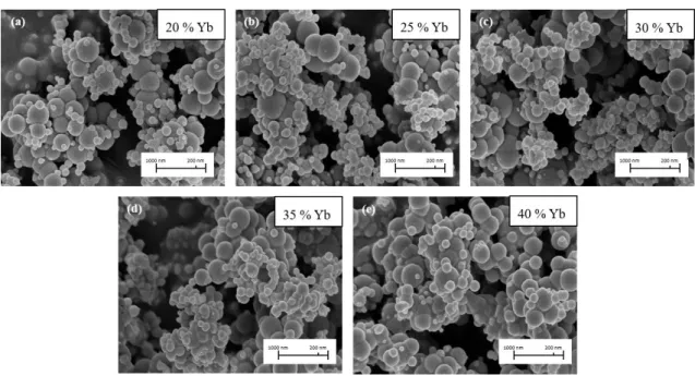
printed in different substrates. (a) Ink printed on paper (IT = 50 ms) and (b) ink printed on glass (IT = 3 ms for commercial marker and IT = 50 ms for developed marker). ... 14 Figure 3.6. Morphology differences between different quantities of urea on the developed marker synthesis. (a) – 0.25 g, (b) – 0.5 g, (c) – 0.75 g, (d) – 1 g, (e) – 1.25 g and (f) – 1.5 g. ... 16 Figure 3.7. XRD diffractogram comparing 0.75 and 1.5 g of urea on the developed marker synthesis. ... 16 Figure 3.8. SEM comparison between several concentrations of Ytterbium in the developed marker (Y2O3:6.5Er). (a) – 20 %, (b) – 25 %, (c) – 30 %, (d) – 35 % and (e) – 40 %. ... 17
Figure 3.9. XRD (a) and PL (b) diffractograms comparing different Yb concentrations. For the photoluminescence data the ink was spread on paper (IT = 10 ms). ... 18 Figure 3.11. PL comparison between different Yb concentrations (a) and synthesis conditions (b) for Y2O3:2.5Yb:0.8125Er . Ink spread on glass for both cases (IT = 5 ms). ... 19
Figure 3.10. PL comparison between different concentrations of Yb. (a) Ink spread on paper (IT = 10 ms). 15 min synthesis at 140 ºC. (b) Ink spread on glass (IT = 10 ms). 1 h synthesis at 180 ºC. ... 19
xvi
Figure 3.12. PL comparison between different annealing temperatures (a) and times at 1000 ºC (b). Ink spread on paper (IT = 10 ms). ... 20 Figure 3.13. PL comparison between different Er concentrations, maintaining the same Yb concentration, (a) and different Yb concentrations, maintaining the same Er concentration. Ink spread on glass (IT = 5 ms). ... 21 Figure 3.14. SEM images of the developed nano-marker (Y2O3:20Yb:6.5Er) to access the size
and structure comparison between (a) CEM Discovery synthesis and (b) CEM Mars One. ... 22 Figure 3.15. Time diagram for nano-particle production. ... 22 Figure 3.16. Blue Wool Scale for the samples tested. (a) 24 h, (b) no exposure and (c) 144 h. . 24 Figure 3.17. Schematics of the detector under the red line glass. In red the LEDs and in black the sensor... 26 Figure 3.18. Detector data acquisition schematics. ... 26 Figure 5.1. Visual comparison between samples before and after environmental chamber exposure (105 ºC, 72 h). ... 36 Figure 5.2. Visual comparison between samples before and after Suntest exposure (340 W, 144 h). ... 36
xvii
Acronyms
UC – Upconversion
UCNPs – Upconverting Nanoparticles INCM – Imprensa Nacional Casa da Moeda REE – Rare-earth elements
PL – Photoluminescence XRD – X-Ray Diffraction
DSC - Differential Scanning Calorimeter SEM – Scanning Electron Microscope RH – Relative Humidity
IT – Integration Time BWS – Blue Wool Scale
xix
Objective
Security inks are commonly used at INCM in their different documents and products. However, these materials are not produced by INCM but outsourced by other companies. Since it was INCM’s interest to produce a new nano-marker with higher security level and at lower cost this thesis has as objective:
• The production of UCNP’s through environmentally friendly techniques such as water-based microwave-assisted synthesis;
• The production scale-up from a 25 ml solution to a 600 ml solution maintaining nano-marker properties;
• Production of a replica of the commercial marker INCM’s acquire since the development of a detector was still being done.
xxi
Motivation
The Earth is a place with many wonders and materials that helped mankind thrive throughout the years. Since the beginning of times, our curious nature led us to explore our planet, as well as the materials it has to offer, in order to shape them into tools to ease our life, which led to the development of several material and processing techniques.
Knowing such techniques of processing and producing materials, turned out to be very profitable hence such innovations made those objects unique and quite difficult to mimic. The lust for the other’s accomplishments led the humankind to start thinking of methods to copy this amazingly design utensils. This was the catalytic agent for the development of forgery techniques.
To make sure the consumer gets the official product from a certain brand, several mechanisms were studied in order to prevent this type of crime, whether it is through some laws or the development of counterfeit identification techniques, such as detection based on overt features, using specific authentication tools and/or specialized knowledge and Forensic analysis[5]. Since physical features of the product are most likely to be copied than a
physicochemical property of the materials used in their conception, products with several physicochemical properties incorporated are prone to be more secure from forgery.
Due to its difficult obtainability and photoluminescent properties, rare-earth elements (REE)[6–8] are extremely interesting to use in such applications as anti-counterfeit agents[9–11]
when mixed with inks. These materials can be synthesised in water-based solutions in a microwave, which make their production fast and environmentally friendly.
When it comes to security, National Mints as INCM are the ones to look at. Being responsible for producing personal documents, bank cards, diplomas, etc. [12], authentication of
some products can only be achieved by via hard to replicate and non-noticeable means. The use of security inks makes this process simple due to its easy application and properties exhibition under certain conditions.
1
1. Introduction
Counterfeiting products are a common problem around the world, since parallel economies emerge from this criminal act and inflict damage in countries’ economies. To not let this happen several techniques were developed[5], from which is important to point out security inks[9–11] that
have in their composition some kind of characteristic and material difficult to replicate.
Addressing the security inks currently marketed there are a lot from where to choose with the most diverse characteristics. These can be Biometric, Solvent Sensitive, Optically Variable, Secondary Fluorescing, Thermochromic, Invisible, Magnetic, Water-Based Fugitive, etc. [13–29]
Secondary Fluorescing inks have a wide range of types in which UC inks are inserted. This kind of security inks are interesting because, compared with other Reactive, Secondary Fluorescing and Invisible inks, the signal is obtained from lower energy electromagnetic waves. UC security inks[30–33] are no novelty in this field but there are some features one can add in the
synthesis process and the process itself that can make it unique to other inks that use this feature. For this, ceramic materials can be used. Yttria (Y2O3) is a sesquioxide, stable in a cubic
bixbyite phase,[34–36] used in several applications, from aiding in sintering processes to
components for REE doped lasers.[34,35,37] Due to its chemical stability and lower phonon energy
this ceramic is interesting when used as host matrix for UC materials.[38–40]
1.1 Upconversion Phenomenon
The UC property expresses the process in which sequential photon absorption leads to the emission of short light wavelengths than the excitation one, process described as an anti-Stokes type emission phenomenon, where the output energy is always superior than the input one.[41]
Theorised in 1959 by the Dutch-American physicist Nicolaas Bloembergen, this concept was to develop an infrared photon detector, using super excitation, to count their interaction with rare-earth or transition-metal ions embedded as impurities in crystalline material. Without the necessary technology at the time, Bloembergen was not able to validate the concept, making François Auzel the first person to witness this phenomenon in 1966, along with Ovsyankin and Feofilov independently.[42]
This enabled advances in the fields of laser and optical technology were possible, allowing alternative technologies to nonlinear optical techniques such as the conversion of low energy laser stimulation into high-energy and long-lasting visible emissions.[43]
2
Upconversion Mechanisms
The mechanism of upconversion can be described by 4 different processes: Excited-state Absorption (ESA), Energy Transfer Upconversion (ETU) and Photon Avalanche (PA).
The ESA process is a multistep excitation by sequential absorption of one or more low-energy photons from the
ground state to the intermediate where the UC emission happens. [10,44–48]
The ETU process is the result of successive energy transfers between ions at different sites. This involves sensitizers and activator ions, where the first one is excited and then transfers energy to the nearest activator ion and exciting it to a higher energy state. The UC emission occurs when the last one drops to ground state. These two should have energy levels with closeness in spatial distance between them. This process has a longer excitation lifetime because of resonant energy absorption.[10,47,49,50]
The PA process only occurs after a critical level of pump density. The high pump density allows intermediate levels to be populated, resulting in an absorption from those levels and leading to the excitation of an ion that will populate an UC level. After this, cross-relaxation energy transfer occurs between excited and ground-state ions. As a result there is an increase in the level population of intermediate and UC emitting levels causing an avalanche effect.[10,47,51– 53]
There is also other process named cooperative UC (CUC) which has the same principle as ETU but the activator does not have adequate long-lived intermediate energy levels compatible to that of the sensitizers.[10]
Upconversion Materials
UC materials usually contain optically active sensitizer and activator ions, generally from d and f blocks.[47] The UC materials performance is directly related to some aspects such as the
host lattice, which determines the distance between the dopant ions, their relative spatial position, their coordination numbers, and the type of anions surrounding the dopant.[54] It is also
important for the host matrices to exhibit low-phonon energies to efficiently avoid degradation of efficiency through nonradiative relaxations and to be chemically and thermally stable. Host
Figure 1.1. Simplified energy level diagrams describing UC processes (red: excitation; blue: UC emission; green: energy transfer). Adapted from[10].
3
materials should also have high tolerance for sensitizer and activator ions and high transparency for free NIR photon migration in the lattice.[10]
Halides and oxides are the most commonly used hosts. The first ones have low phonon vibration energy, with the drawbacks to their application their toxicity and air-sensitivity (e.g. YF3). The latter have enhanced chemical stability and are eco-friendly, yet they suffer from high
phonon energy (e.g. Y2O3).[54–56] However a suitable dopant-host pair must be selected to achieve
the proper control in the energy transfer process.
The sensitizers are responsible for transferring energy to the activator, so they must have similar resonant energy levels with suitable excited energy state located in the NIR region. Among all the RE ions, Yb3+ is the best choice as a sensitizer since the energy level diagram of
Yb3+ has only one excited state (2F
5/2), which matches very well with the f-f transitions of many
RE activators.[10,47,57–62]
By increasing the activator ion concentration, it is possible to increase UC emission but only to a certain point. Beyond a critical concentration the system starts to quench and the emission stops increasing. However, this quenching phenomenon can be solved by increasing the sensitizer concentration while maintaining the activator concentration at lower levels.[10,62,63]
Other than d and f block elements, there are some organic materials susceptible to exhibit this property.[56]
Despite its application on security, other technologies can take advantage of this property such as photovoltaic cells[56] and biomedicine[64–68], since dispersible upconverting
nanophosphors show low cytotoxicity and Near Infrared (NIR) light causes very low auto fluorescence background of the biological materials, making them possible substitutes for organic dyes and quantum dots in biological tagging experiments. However studies must be made regarding the aggregation of this materials within cells and tissues. [54,69]
1.2 Phosphorescence
The phosphorescence is a photoluminescent process in which a material, previously excited with photonic energy, re-emits the radiation absorbed in a certain period. This type of phenomenon is associated with forbidden energy state transitions[70–72], in which electrons that have absorbed photons
cross into higher spin multiplicity energy states, usually triplet states.[73,74] These transitions are not kinetically favourable, thus
their slow degradation to the ground state. Figure 1.2. Energy scheme on the mechanism of fluorescence and phosphorescence. Adapted from[74].
4
As in the UC phenomenon, phosphorescent materials must have a host matrix and an element (activator) added as dopant, that is responsible for the afterglow (e.g. Y2O3:Eu[75,76]) and can also
be applied in the security inks field.[77–79]
1.3 Nanoparticle Synthesis Techniques
Due to the necessity to increase its efficiency, the synthesis of this materials turned out to be crucial to achieve a heterogenic dispersion and surface modification. Several techniques are used such as Coprecipitation, Hydrothermal, Microwave-assisted synthesis and Sol-Gel.[10,65,80–83]
The hydrothermal synthesis can occur in a water-based system with low reaction temperature. This method heats the solution at high pressure above its critical point. It is used when controlled nanoparticle size and shape is desired, parameters controlled by reaction temperature and time and surfactant type, which is the great advantage of this type of synthesis.[10,66,84]
The microwave-assisted method relies on microwave radiation to heat any solution containing mobile electric charges by the interaction between the particles in solution and the electromagnetic waves.[82,85–89] Used for the nano-powder formation, the reagents in water
solution, are placed inside the microwave where the synthesis will take place. Because water is a dielectric the microwave energy is absorbed, and heat is generated, which allow nanoparticles to form.
Over other techniques the microwave-assisted hidrothermal synthesis is more interesting due to its need of no shophisticated equipents to treat synthesis residues and fumes, which makes this type of method highly environmental friendly, the synthesis velocity, process cheapness and homogeneous particle morphology .[10,65,81,90]
After the synthesis, particles must undergo through an annealing process, fundamental after the chemical process to convert into the final phase and structure, increasing crystallinity and thus removing the solvents. [10,81,91,92] These processes were used in the synthesis of Yttrium
oxide, following the equations[83,93–96], where the annealing process is revealed to be necessary
for Yttria formation:
2𝑌3++ 7𝐻
2𝑂 + 3𝐶𝐻4𝑁2𝑂 → 2𝑌𝑂𝐻𝐶𝑂3+ 6𝑁𝐻4++ 𝐶𝑂2 (1.1)
2𝑌𝑂𝐻𝐶𝑂3
𝑠𝑦𝑛𝑡ℎ𝑒𝑠𝑖𝑠
5
𝑌2𝑂2𝐶𝑂3𝑎𝑛𝑛𝑒𝑎𝑙𝑖𝑛𝑔
→ 𝑌2𝑂3+ 𝐶𝑂2 (1.3)
1.4 Anti-counterfeit Ink Production
For producing the nano-powder marker for the security ink other elements must be added to the synthesis. The increase of the number of dopants makes the product harder to replicate, proving to be essential for this application. For this reason, and for its difficult obtainability[6–8],
two RE were selected to dope the Y2O3 matrix: Yb and Er.
After the synthesis, the nano-powder must be added to the ink, that will serve as a vessel for its application. Adding pigments may be a problem since they can diminish the intensity of the UC light, leading to a lesser choice of colours to be implemented in the final product.
By developing this product for INCM, it is possible to give the company a way to produce its own security ink in a cheaper way and with more security than the commercial ink acquired. However, the commercial ink has the advantage of having a portable and easy to use detector that measures the properties of the ink wherefore reverse engineer was used on the detector to make a new one suited for the developed ink.
Since INCM is responsible, among other things, for tobacco seals which grants the product authenticity and allows its legal sell, the development of a new ink and detector enables INCM to produce its own signature ink and permit its easy reading in every product. Cheap production prices are also seductive when producing the marker.
7
2. Materials and Methods
2.1 Nano-marker Production
This study started with the investigation of the commercial marker purchased by ICNM. The “inverse engineering” was conducted with structural characterization of this commercial material. A marker is a substance with a specific characteristic that is added to the ink in order to grant it some level of security, in this case Yttria nanoparticles doped with Ytterbium and Erbium.
Knowing that the commercial marker had Y and Yb, the starting point was to know how to synthesise a similar product and which RE to add to make the marker more secure. To achieve the main goal of producing a nano-marker, durable and more secure than the commercial one, several experiments were conducted.
Having chosen Er as the second dopant for the development of the new marker the synthesis process was initiated. The nano-particles were produced using hydrothermal synthesis assisted by microwave radiation.
The starting reagents were N3O9Y ‧ 6 H2O (99.8% purity), N3O9Yb ‧ 5 H2O (99.9% purity),
Er(CH3CO2)3 ‧ 4 H2O (99.9% purity) and urea (CH4N2O) from Sigma Aldrich used without
further purification.
For the development of the nano-marker it was fixed the Y concentration at 0.05 M which was dissolved in 40 ml of water. Then 20 % of Yb, 6.5 % of Er (molar percentage of Yttrium) and 1.5 g of Urea were added, all dissolved in 20 ml of water each. The reagents were then mixed together to make 100 ml of solution.
For other studies, the concentration of N3O9Y ‧ 6 H2O was fixed at 0.05 M and the other
components varied as presented below:
• For studying the influence of Yb, it was used Y2O3:xYb having x ranging from 1.5,
2, 2.5, 5, 10, 12.5, 15, 20, and 25 mol.%.
• When fixing Er, it was used Y2O3:xYb:6.5Er having x ranging as 20, 25, 30, 35 and
40 mol.%.
• With Yb fixed: Y2O3:2.5Yb:xEr having x ranging as 0.3125, 0.8125 and 1.3125
8
The materials are named regarding the amount of each element presented. Nevertheless, the produced nano-markers at CENIMAT/i3N will be hereafter called developed nano-marker, while the one purchased by INCM, will be called commercial marker.
It has also been investigated the effect of the amount of urea to correlate with the structural properties of the nano-markers where this reagent was added from 0.25 g to 1.5 g (increasing 0.25 g up to a maximum of 1.5 g).
Each solution was prepared using water as solvent. Then, the syntheses were conducted at 140 ºC for 15 minutes and 180 ºC for 60 minutes in two different microwaves systems. Figure 2.1. (a) shows the CEM Mars One and the CEM Focused Microwave Synthesis System Discover SP is represented in Figure 2.1. (b).
Since the Mars One had the capacity to synthesize 600 ml (separated in 12 vessels of 50 ml each) at a time, whereas Discovery system could only synthesize 25 ml, the former equipment was used for scaling up the process considering that one of the objectives was to assure reproducibility at industrial scale. The nano particles produced were centrifuged at 4000 rpm and washed 3 times with distilled water and 3 times with isopropanol (IPA - C3H8O). Afterwards,
the powder was dried at 60 ºC for 1 h before the annealing process.
The dried powder was exposed to 700 ºC for 7 h (1 h ramp for reaching the temperature and 6 h holding it) and to 1000 ºC for 2, 4, 6 and 12h (1 h ramp for reaching the temperature). This process was fundamental to convert the synthesized powder into its final phase and structure, increasing crystallinity and thus removing the solvents.[10,81,91,92] The matrix production followed
the equations (1.1), (1.2) and (1.3) and the final product the following equation:
Figure 2.1. Microwave equipments used for synthesis, (a) CEM Mars One and (b) CEM Discovery SP @ http://cem.com/discover-sp
9
2𝑌(𝑁𝑂3)3(𝑎𝑞) + 𝑌𝑏(𝑁𝑂3)3(𝑎𝑞) + 𝐸𝑟(𝐶𝑂𝑂𝐶𝐻3)3(𝑎𝑞) + 𝐶𝑂(𝑁𝐻2)2(𝑎𝑞) → 𝑌2𝑂3: 𝑌𝑏: 𝐸𝑟(𝑠) + 13 2 𝐻2𝑂(𝑔) + 4𝑁2(𝑔) + 4𝐶𝑂2(𝑔) + 15 2 𝑂(𝑔) (2.1)Despite the results for the ink quantity, the concentration was fixed at 1:2, which mean a ratio of 1 g of nano-powder to 2 g of ink. The ink used is Apollo NUV 10520 Transparent White from Apollo Colours Limited, a polymeric ink cured by UV light. From this point on, the ink will be called Blank Ink.
The mixing process was carried out manually, with the direct addition of the powder into the ink. The complete ink with the nano-powder was then printed at INCM with the IGT printability tester (Figure 2.2.) and assessed with the commercial ink supplier’s detector and software.
2.2 Characterization
The morphology of the materials was studied using a SEM-FIB microscope AURIGA from Carl Zeiss (5 kV). The microscope is coupled with an energy dispersive X-ray spectroscopy (EDS) detector.
Scanning Transmission Electron Microscopy (STEM) analyses of the nanostructures
was carried out at 300 kV with a FEI Titan G2 60-300 instrument equipped with a DCOR
probe Cs-aberration corrector and a Super-X Bruker energy dispersive spectrometer
with 4 silicon drift detectors.
XRD analyses were used to assess materials phases and crystallinity on PANalytical's X'Pert PRO MRD with Cu Kα radiation (λ = 1.5405 Å, Scan Step = 0.0334 º, Time Scan = 33,02 º/min). DSC measurements were carried out to the obtained powder, before annealing. It was used a Simultaneous Thermal Analyser TGA_DSC_STA 449 F3 Jupiter, from Netzsch. Approximately 5 mg of powder was loaded into an open PtRh crucible and heated from room temperature to 1000 ºC, with a heating rate of 10 ºC/min under atmospheric conditions.
Photoluminescence were also examined with a 976 nm laser (Avantes NIR light, Iso-Tech power source 1W, 5 nm resolution) between 880 and 1800 nm. For phosphorescence, the lifetime of the marker was measured with a 976 nm laser (Germanium detector – PDA50B-EC – Iso-Tech power source 1W. Shutter frequency of 150 rps).
Figure 2.2. IGT printability tester @ http://www.igt.nl/igt-testers/graphic/c1-5
10
2.3 Quality Characteristics Evaluation
Prior to mass production, quality characteristic trials are crucial to ensure that the products behave accordingly to the expected in every possible situation. For this evaluation, several samples with printed blank ink, commercial marker and developed marker were prepared using the IGT, in a total of 29 samples of each. Every printed sample was then divided into six equal parts (one of which was stored to serve as pattern for later comparison).
After choosing the parameters to evaluate in the test chambers, the samples were randomly chosen (in packs of 5 for each sample) and put in the testing area, in order to access their behaviour.
Table 2.1. Accelerated Aging tests for the developed and commercial markers. In black, exposure times that were not assessed according to the ISOs used.
For these tests it was used an Aralab Environmental Chamber for the climatic trials and the Atlas Suntest XLS+ for the sun exposure simulation. Concerning the last one, once there was no means to compare the exposure time with the real one, indirect methods of analyses were used such as the blue wool scale [102–105] and the energy a sample receives per day.
The blue wool scale relies on the lightfastness of a known pigment to estimate the exposure time. For the second method the RETScreen Expert [106] was used to determine the amount of
energy the sample would endure per day in Lisboa. This software is used for photovoltaic dimensioning, so this energy was determined by assuming the sample would get the same amount as a photovoltaic cell.
24 h 48 h 72 h 144 h 168 h 80 ºC 65 % RH[97] x x x x 105 ºC 20 %RH[98] x x x x 150 ºC 20 %RH[99] x 120 ºC 20 %RH[99] x 25 ºC 90 % RH x x x x -20 ºC 20 % RH x x x -20 ºC 80 % RH x x x 340 W/m2[100,101] x x
11
3. Results and Discussion
Despite the success on producing a new and more secure nano-marker, the drawback of not knowing what the detector was measuring made the production of a replica from the commercial marker a need, since INCM could be able to replicate if the price reduction justified that option. By trying to replicate the commercial marker several analyses were made concerning the effect of nanoparticle composition and synthesis and annealing time and temperature in the optical properties.
Studying the effect of Yb, Er and urea in the nano-marker was still needed to understand if the direction took in the beginning of this work was the correct. Since the nano-marker will be used in an industrial scale, ramping up the process maintaining the same characteristics is crucial.
3.1 Developing the nano-marker
The production of a new nano-marker (Y2O3:20Yb:6.5Er) implied the study of this marker
characteristics for the later development of the detector. Since it was the best interest to make this production as cheap as possible, the percent yield had to be calculated in order to have a perception of how much reagent was being used per synthesis.
With equation (2.1), it is possible to calculate the theoretical mass of the powder obtained which was 0.7968 g. The value obtained has only at account the mass of the elements that are present in the final product, which can mislead on the percent yield calculation. For each 100 ml synthesis produced, 0.76 g of nanoparticles were obtained, making a yield of 95.38 % recurring the equation (3.1). This percent yield is the same for both microwaves.
𝜂 = 𝑚𝑟𝑒𝑎𝑙
𝑚𝑡ℎ𝑒𝑜𝑟𝑖𝑐𝑎𝑙
× 100 (3.1)
The value obtained is important because it indicates that the reaction used the reagents needed at its fullest, having wasted little amounts of it.
Once the powder is microwave synthesized, it was mixed with the blank ink. Grinding the powder before mixing can benefit the mixture and application on substrate. When not grinded the powder can be stuck on the IGT (Figure 2.2) rolls and not printed, making the printing substrate poor on nano-marker. It was observed that the nano-powder size in the mixed ink did
12
not influenced the detector reading but its dispersion had a great influence, so the particle size reduction or a better way to spread the particles is needed to extract the better properties of the marker produced.
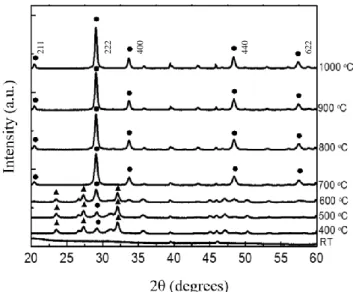
Annealing Temperature
Figuring which annealing temperature to use for sintering the Y2O3 nano-particles in-situ
XRD was used. In Figure 3.1. it is observed that Y2O3 matrix is fully crystalized at 700 ºC
through the XRD characteristic peaks of this oxide.
Fixing the annealing temperature at 700 ºC is an advantage when addressing production cost because, from every studied temperature, this is the lowest at which Y2O3 crystalizes. Later when
producing the replicas and with the developments in the detector studies, 1000 ºC will be used.
Ink Quantity
It was important to determine the amount of power to be added to the blank ink, so Differential Scanning Calorimeter (DSC) measurements were carried out in the commercial marker. In Figure 3.2., it was possible to determine the concentration of marker composing the ink through the mass loss, i.e. 20 % of materials
remaining after experiments. Figure 3.2. Determination of nanoparticles quantity in commercial ink through DSC analyses (mass loss comparison between inks).
Figure 3.1. In-situ XRD diffractograms heat exposed up to 1000º C. The circles represent the yttrium oxide phase and the triangles carbonate phases. Standard data from JCPDS card 43-1036.
13
As explained in section 2.1., despite the results the ink/nano-marker ratio was kept at 1:2 respectively. The blank ink and nano-marker mixing had an important role on data acquisition.
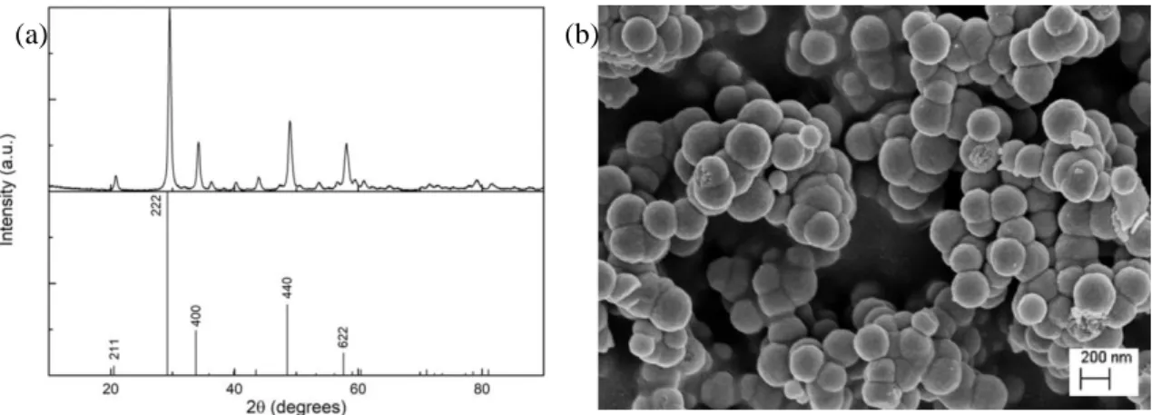
Developed nano-marker
Addressing the morphology and particle constitutions, SEM images and XRD data was obtained. Through these, one can observe the particle size and morphology and if it was indeed formed the desired product.
From the SEM images it is possible to see that after synthesising the material it was obtained spherical particles with sizes in the nanometre scale. This particle dimension is favourable when using these markers for security because advanced and expensive are required to observe them.
The XRD plot in Figure 3.3. confirms the presence of cubic Y2O3, and it can be assumed
that no second phases were formed.
It is possible to determine crystallite size (τ) resorting to the Scherrer equation (3.2) by the data provided in the XRD analysis, where K is the shape factor (0.89)[107], λ the X-ray
wavelength (1.5405 Å), β the full width at half maximum and θ the Bragg angle:
𝜏 = 𝐾𝜆
βcos 𝜃 (3.2)
Using the most intensity peak, we have a crystallite size of 15.6 nm. TEM images (Figure 3.4.) were obtained to confirm the crystalline size value obtained with Scherrer equation (3.2). It can be observed that the sphere is composed by smaller internal grains forming a compact agglomerate.
Figure 3.3. Developed nano-marker (Y2O3:20Yb:6.5Er) XRD diffractogram (a), together with the simulated Y2O3
phase, and SEM image (b). Standard data from JCPDS card 43-1036.
14
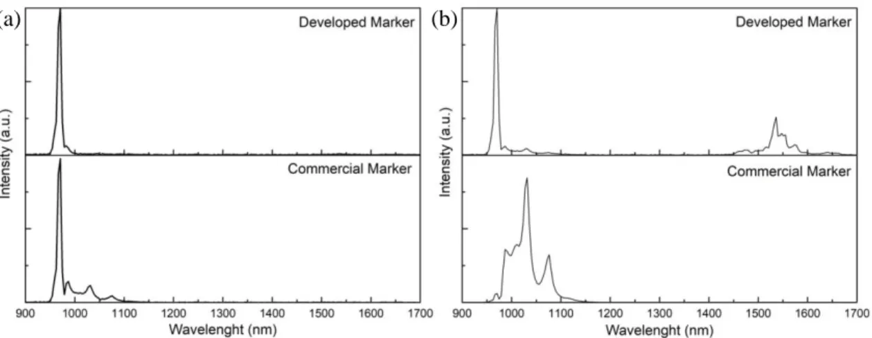
In a first approach, regarding optical properties, IR photoluminescence tests were conducted since this was the parameter believed to be analysed by the detector. For this property the developed marker was compared with the commercial, as seen on Figure 3.5.. The most intensity peak around 960 nm is due to the light filter used in the data acquisition set-up.
Addressing the glass printed nano-marker (Figure 3.5. (b)), it is possible to observe characteristic peaks for both elements (Yb and Er). In the commercial marker, Yb peaks appear at 980 and 1030 nm[108–110] associated to transitions from 2F
5/2 level to 2F7/2 energy
level,[10,36,108,111,112] and exhibiting a green light under a 976 nm laser.
When analysing the PL behaviour of the developed marker, the Er peak is easily observed at 1530 nm.[113–116] Despite having Yb in its constitution the Yb:Er ratio chose can be responsible
Figure 3.4. Developed nano-marker (Y2O3:20Yb:6.5Er)
TEM image.
Figure 3.5. PL comparison between developed (Y2O3:20Yb:6.5Er) and commercial marker printed in different
substrates. (a) Ink printed on paper (IT = 50 ms) and (b) ink printed on glass (IT = 3 ms for commercial marker and IT = 50 ms for developed marker).
15
for the intensity decreasing of Yb peaks[111], which translates in undefined peaks from 980 nm
to 1070 nm. However, peaks with most intensity in that range appear at 980 and 1030 nm, indicating the Yb PL. When exposed to a 976 nm laser, the developed marker exhibited a red light that can be explained, according to Singh et al.[36], by the energy level transitions 4I
15/2 (Er3+)
and 2F
5/2 (Yb3+) to 4I11/2 (Er3+) and 2F7/2 (Yb3+) through energy transfer from Yb ions, 4I11/2 (Er3+)
and 2F
5/2 (Yb3+) to 4F7/2 (Er3+) and 2F7/2 (Yb3+) through energy transfer from another Yb ions,
then 4F
7/2 to 2H11/2 and 4S3/2 to 4F7/2 as non-radiative decay through multi phonon relaxation and
finally 4F
9/2 to 4I15/2 where the red wavelength are emitted.[10,36,111]
The overlap between Yb3+ and Er3+ absorption cross-section and Yb3+ and Er3+ emission and
absorption bands respectively result in an efficient energy transfer between both elements.[10,36]
When printed on paper (using the IGT), evidences of the Yb presence in the commercial marker can be noticed through the peaks from 980 nm to 1070 nm. However, since the PL data acquisition is dependent on the analysed material quantity significant difference between both printed methods can be attended. In the developed marker a tenuous Er band can be observed but is so weak that one can only despise it.
It is important to be noted that, the developed marker mixed in the ink was grossly dispersed, so the glass-printed ink can suffer from marker shortage. The same happened with the paper-printed ink, due to some powder attachment to IGT rolls, which reduced the amount of material available for measurement. Despite the mixing problem it is still possible to observe these peaks even if tenuous.
This can also explain the difference in the Integration Times (IT) for both markers printed on glass, since less quantity of nano-marker and not homogeneous spreading requires higher times for acquiring PL signal.
When analysed with the INCM detector and respective software the developed marker exhibits signal but appear as “other tag” as expected, in contrast to the “tag08” signal that the detector exhibits when analysing the commercial marker. This “tag08” is the commercial marker signature from the suppliers.
Due to these results, there is no possible way to appraise the developed marker thus the necessity of developing a detector capable of this feat.
Urea Influence
As observed in Figure 3.6., spherical structures were obtained, and urea was the responsible for the spherical morphology. Being the second most used reagent, parallel studies were conducted to analyse its influence. To make this study, the formula for the developed nano-marker was used (Y2O3:20Yb:6.5Er) and the urea quantity increased from 0.25 g to 1.5 g.
16
From Figure 3.6., it is also possible to observe that for urea amounts under 0.75 g, the nanoparticles were largely heterogenous in size and in some cases the particles were not perfectly spherical. No differences were observed for amounts over 0.75 g, which appears to be the minimal amount necessary to produce homogeneous materials.
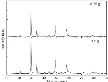
Figure 3.7. demonstrates the XRD measurements of Y2O3:20Yb:6.5Er materials synthesized
with 0.75 and 1.5 g of urea, in which any difference could be observed regarding the urea used. Again, the pure Y2O3 phase was observed.
Figure 3.7. XRD diffractogram comparing 0.75 and 1.5 g of urea on the developed marker synthesis.
Figure 3.6. Morphology differences between different quantities of urea on the developed marker synthesis. (a) – 0.25 g, (b) – 0.5 g, (c) – 0.75 g, (d) – 1 g, (e) – 1.25 g and (f) – 1.5 g.
17
With both results from Figure 3.6. and Figure 3.7. it is possible to assure that the urea quantity reduction can be made without affecting the developed marker structural properties. However, for further studies the quantity was fixed at 1.5 g.
Ytterbium Influence
To understand the influence of the concentration of Yb in the developed nano-marker, several molar concentrations were tested having the Er amount fixed (Y2O3:xYb:6.5Er). From
SEM analyses, it is possible to verify that every condition analysed resulted in spherical particles, however with the increase of Yb, it could be observed the formation of smaller particles resulting in heterogenous particles in size (Figure 3.8.).
Comparing the XRD diffractograms for every concentration it is possible to confirm that Y2O3 still forms for higher amounts of Yb. By increasing the quantity of Yb it is expected the
increase of Er PL intensity due to ETU phenomenon which can be observed in Figure 13. (b).[10,62,63] Despite this increase, the characteristic peak from Yb is not greatly evidenced.
The structural characterization of the materials produced with different amounts of Yb, allowed to confirm that the lowest concentration of Yb is the most inciting considering the price for producing the nano-marker increases with the use of REE.
Figure 3.8. SEM comparison between several concentrations of Ytterbium in the developed marker (Y2O3:6.5Er).
18
It is important to notice that with the increase of Yb quantity, the Er intensity peak is more pronounced (~1530 nm). This phenomenon can be explained by the ratio between Yb/Er concentrations, which has an influence in the signal obtained. [10,62,63] For getting a better signal
the REE ratio in the developed nano-marker (Y2O3:20Yb:6.5Er) can be rethought to achieve
more defined Yb and Er peaks, when addressing PL characteristics.
3.2 Replica Production
Not being able to evaluate the behaviour of the developed nano-marker using the detector, despite getting a reading as “other tag”, commercial marker replicas were made. To synthesize this product, Erbium was removed from the synthesis process while the remaining reagents were mixed using the same process.
To achieve the replica several tests were conducted from changing annealing and synthesis temperature and using different Yb concentrations (Y2O3:xYb).
Ytterbium Influence
When tested for PL, it was observed that, by reducing the amount of Yb, the signal increased (Figure 3.10.). However, the commercial marker’s intensity was never reached. The commercial marker and the replicas developed cannot be compared due to differences in the IT for both measurements (3 ms for the commercial marker and 10 ms for the replicas developed). Since the commercial marker had a bigger particle size than the developed one the synthesis time and temperature was increased to achieve this property (1 h at 180 ºC).
Figure 3.9. XRD (a) and PL (b) diffractograms comparing different Yb concentrations. For the photoluminescence data the ink was spread on paper (IT = 10 ms).
(b) (a)
19
Due to shortage on Yb there was no possible to synthesise the whole range of concentrations for the 180 ºC synthesis.
For both cases the best signal was obtained by decreasing the Yb concentration. Reducing the concentrations even further had no improvement on the PL signal so 2.5 % Yb was maintained (Figure 3.11. (a)) for further studies.
No direct comparison can be made between the charts on Figure 3.10. due to the influence of the quantity of material analysed, one cannot assure that this alteration had better results. Evaluating the replica with 2.5 % Yb in the same conditions and synthesized at different conditions it was observed that PL signal benefited from higher synthesis times and temperatures (Figure 3.11. (b)).
No Yb concentration passed in the detector (no “tag08” exhibited) despite giving signal. (b)
(a)
Figure 3.11. PL comparison between different concentrations of Yb. (a) Ink spread on paper (IT = 10 ms). 15 min synthesis at 140 ºC. (b) Ink spread on glass (IT = 10 ms). 1 h synthesis at 180 ºC.
(a) (b)
Figure 3.10. PL comparison between different Yb concentrations (a) and synthesis conditions (b) for Y2O3:2.5Yb:0.8125Er . Ink spread on glass for both cases (IT = 5 ms).
20
Annealing Temperature
The influence of the annealing was studied as well, since no replica passed in the detector as the commercial marker. It was observed an increase in the PL signal when higher synthesis temperatures were reached so, by increasing the annealing temperature one expected to observe the same relation. For this the synthesis time and temperature were fixed at 15 min at 140 ºC and the 2.5 % as Yb concentration.
It was confirmed that higher annealing temperatures had a significant impact on PL signal (Figure 3.12. (a)) increasing the exhibited Yb peak.
When assessing the annealing time effect in the PL readings it was observed that 12 hours had the best results. However, this was not expected and for this time, the value should be the lowest considering the other times, according to the detector readings present in Table 3.3. in a later section. This discrepancy regarding the measured data might be due to better reading angles or larger quantities of nano-marker for this specimen when analysed. Given this data from the detector the trend should be after and before 4 hours for the PL reading to decrease, being this time the one with the highest intensity.
Erbium Influence
Since good results were obtained when reducing the quantities of Yb it was interesting to observe the behaviour of the nano-marker with reduced dopant concentration. This was studied by maintaining the proportion used for the developed marker (20 % Yb to 6.5 % Er), fixing the Yb concentration at 2.5 % and varying the Er concentration. The synthesis time and temperature used were 1 h and 180 ºC.
(a) (b)
Figure 3.12. PL comparison between different annealing temperatures (a) and times at 1000 ºC (b). Ink spread on paper (IT = 10 ms).
21
The relation used initially, is the best option in terms of PL since reducing or increasing the Er concentration the intensity is reduced. Reducing Yb concentration makes the nano-marker Yb and Er peaks loose PL intensity for the integration time analysed, excluding the possibility to alter this relation (Figure 3.13. (b)).
It was expected the PL signal improvement by increasing the Yb:Er ratio[10,62,63], but that
wasn’t observed maybe because the low quantity of REE used.
3.3 Scale-Up and costs
Having the developed marker synthesis established, the arrangements for the scaling-up were studied. Since the CEM Discovery (Figure 2.1. (b)) has only the capacity of synthesising 25 ml of solution per synthesis a microwave with a greater capacity was needed. That way, the CEM Mars One (figure 2.1. (a)) was used for this purpose. Having a capacity of 600 ml per synthesis, this one could operate at full capacity or utilizing only the needed vessels (up to 50 ml each).
Swapping microwaves was not linear as the specifications of the larger one were different. By having a limited synthesis quantity, CEM Discovery synthesis parameter were fixed for every trial whereas CEM Mars One parameters needed to be checked for every trial, since every little difference in the quantities for which the microwave was set up to, had influence in the linearity of the synthesis temperature. On account of this aspect, to maintain the same synthesis time and temperature it was needed to understand the microwave behaviour when holding the vessels.
The quantity of vessels held in the microwave played a significant role on what parameters to use, so for every combination of vessels they had to be changed. For using the microwave full
(b) (a)
Figure 3.13. PL comparison between different Er concentrations, maintaining the same Yb concentration, (a) and different Yb concentrations, maintaining the same Er concentration. Ink spread on glass (IT = 5 ms).
22
capacity, the synthesis was carried in 2 steps (at 1000 W each) – 80 ºC for 5 minutes and 140 ºC for 15 minutes. To reach every step a ramp time of 10 minutes was needed.
In Figure 3.14. one can perceive no structural difference between both microwave synthesis. Having achieved this step, it is possible to save a lot of time to make the same quantity of nano-particles by using CEM Mars One.
Taking in account every process since the solution preparation to the annealing the whole process takes about 8.4 hours from start to finish as described in Figure 3.15..
In a single day (8-hour work day) it is possible to make 10 microwave synthesis and have them ready for the annealing, that can be done in the end of the shift, leaving the oven working until the next day. In order to produce 1 kg of nano-particles it would take 23 days.
The following table expresses the quantity of reagents needed and its cost for making of 1 kg of powder. Buying these reagents in bulk/industrial scale can reduce the overall price.
Figure 3.15. Time diagram for nano-particle production.
Figure 3.14. SEM images of the developed nano-marker (Y2O3:20Yb:6.5Er) to access the size and structure comparison
23
Table 3.1. Producing quantities and costs for developed marker (Y2O3:20Yb:6.5Er) and replica (Y2O3:20Yb)
Developed Marker Replica
Quantity (kg) Cost (€) Quantity (kg) Cost (€)
Yttrium Nitrate 2.88 2231 2.88 2231
Ytterbium Nitrate 0.68 2254 0.68 2254
Erbium Acetate 0.20 1205
Urea 2.25 272 2.25 272
Total (€) 5962 4757
Looking at the previous table and comparing with the price of the commercial marker (1165€ per ink kilo) one can observe that, for the budget obtained, the developed marker the price for kilo of ink with the nano-marker would cost about 1987€ and the replica 1586€.
3.4 Accelerated Aging
For studying the behaviour of the developed nano-marker (Y2O3:20%Yb:6.5%Er) to some
conditions several test samples were produced. Not being able to get a reading for the developed marker in the detector and knowing the it had similar characteristics to the commercial one, conclusions were made by analysing the commercial marker response after each condition.
For each condition studied (on Table 2.1.) it was subdued a set of 15 samples of commercial marker, developed nano-marker and only ink (5 samples each).
Environmental Chamber
When submitted to environmental chamber, for every criterion, samples lost brightness and kept structural integrity (Figure 5.1.). When read in the detector, the commercial marker exhibited no difference in the readings.
Despite the visual differences, by these data one can conclude that humidity and temperature doesn’t affect the signal read by the detector, which is good regarding the material life time.
Suntest
The amount of radiant energy (J/m2) received by the samples in the Suntest is given by the
24
𝐻 = 𝐸 × ∆𝑡 (3.3)
For the exposures described in Table 2.1. the radiant energy is 29.38 MJ/m2 and 176.26
MJ/m2 for 24 h and 144 h respectively using the window glass filter. Making use of the
RETScreen Expert, for exposures in Lisboa, Portugal, the average daily solar radiation is 16.78 MJ/m2, so it was expected that 144 h (6 days) of exposure to mimic 10.5 days of real time
exposure.
When assessing the time spanned in the Suntest chamber with the Blue Wool Scale (BWS) the time gave is different.
According to equation (3.4), which gives the amount of lux depending the power, for the power and time exposed in Figure 3.16. (a) only the level 1 of the BWS should be faded (𝐸𝑣≈
0.3 Mlx). [104,117]
𝐸𝑣(𝑙𝑥)= 𝑃𝑊× 𝜂(𝑙𝑚/𝑊) / 𝐴(𝑚2) (3.4)
The luminous efficacy (𝜂) for arc xenon lamps ranges between 30 and 50 lm/W[118] and since no information on this parameter from the producer
was given, an intermediate value was used (𝜂 = 40 lm/W).
Contrary to calculations the BWS reached higher levels than expected, with the condition (a) reaching level 4 and the condition (c) reaching level 6. The discrepancy between the calculated values by both methods and the BWS can’t be explained and only with real time studies this effect can be assessed.
As for the visual aspect of the samples tested, for both times no degradation of the samples was observed besides their yellowing as observed for the Climatic Chamber samples. As for the samples previously mentioned the commercial marker still exhibited no difference when read.
Regarding the differences in colour the samples were examined with the L&W Elrepho. The following table gives the ∆𝐸𝑎𝑏∗ of some conditions according to equation (3.5). The difference in colour is confirmed if ∆𝐸𝑎𝑏∗ > 2.3.[119]
∆𝐸𝑎𝑏∗ = √(𝐿∗2− 𝐿1∗)2+ (𝑎2∗− 𝑎1∗)2+ (𝑏2∗− 𝑏1∗)2 (3.5)
Figure 3.16. Blue Wool Scale for the samples tested. (a) 24 h, (b) no exposure and (c) 144 h.
25
Table 3.2. Colour difference between some sample’s exposed and non-exposed states. These Lab values are Lab averages from the samples exposed to these conditions. D65 and C standard illuminants[120,121] used due to equipment
specifications.
Developed Marker Commercial
Condition Before After ∆𝐸𝑎𝑏∗ Before after ∆𝐸𝑎𝑏∗
105 ºC 20 % RH (72h) D65 L* a* b* 93.97 93.13 8.43 93.10 93.13 7.85 1.16 -1.00 0.79 -1.00 -5.77 2.34 -5.30 2.34 C L* a* b* 93.56 93.01 6.38 92.71 93.04 6.22 0.69 -1.43 0.46 -1.43 -2.32 3.67 -2.25 3.67 340 W/m2 (144h) D65 L* a* b* 93.94 91.00 17.08 93.65 91.00 16.54 1.25 -2.03 0.83 -2.03 -5.99 10.51 -5.56 10.51 C L* a* b* 93.52 91.20 13.55 93.25 91.20 13.20 0.78 -2.91 0.43 -2.91 -2.48 10.35 -2.26 10.35
Studies regarding the influence of some solvents in the nano-marker must be done in order to have a broader view of the conditions that affect its reading.
3.5 Detector
For sample control, a detector supplied by the commercial marker producer is used after printing the ink in the substrate. Since this was a security tool, every device provided by the company had a code in which only the fingerprint of the acquired marker exhibits a green light with “Tag08” (supplier name for the commercial nano-marker), despite recognising similar synthesised markers, where it exhibits an orange light with “other tag”.
The equipment used at INCM is a fine work of engineering and so is very robust and hard to recreate due to some of the components being tailor made for it. Even though it was a difficult task to comprehend the device performance, this was a fundamental point to get an idea on which property was being analysed by the detector.
Since there was no way to assure the produced marker was working as previously thought, the device was reverse engineered to enable other markers to be read.
26
Having it figured out, it was able to comprehend this device’s behaviour. Samples are set above the 2 windows in the detector where they get analysed. The window with no red line has a motion sensor that triggers the detector to operate. Once triggered, the 2 LEDs (Figure 3.20.) under the red lined window excite the sample and the signal is received by a sensor. This window’s glass filters visible light.
By understanding how it works, it was possible to know what material characteristic to focus to get the best marker possible to be read by the machine.
The equipment measured phosphorescence (intensity difference between light emission state and no emission state) through the voltage difference between 2 states.
Since no sample was tested for phosphorescence, by connecting the device to an oscilloscope one was able to measure the voltages for both states and understand which way to go. This was a problem when producing the replica because only in a later state of this investigation this parameter was a concern.
The detector turned the LEDs on and the sample is excited. Then the LEDs turn off and two measurements are made (t1 and t2) that give information on the sample’s lifetime.
To measure this parameter a crocodile clip was connected to the ground and the probe in the measuring sites.
Figure 3.17. Schematics of the detector under the red line glass. In red the LEDs and in black the sensor.
27
Table 3.3. Oscilloscope readings. 1 – Synthesis 15 min at 140 ºC. 2 – Synthesis 1 h at 180 ºC.
Marker Tension 1 (V)/ t1 Tension 2 (V)/ t2
Commercial 4 3 Y2O3:2.5Yb annealed at 700 (6 h)1 3 2 Y2O3:2.5Yb annealed at 700 (6 h)2 2.8 2 Y2O3:20Yb annealed at 1000 (2 h) 3.8 2.2 Y2O3:20Yb annealed at 1000 (4 h) 3.8 2.6 Y2O3:20Yb annealed at 1000 (6 h) 3.8 2.4 Y2O3:20Yb annealed at 1000 (12 h) 3.8 2
It is observed that by increasing the annealing temperature one can get closer to the values from the commercial marker, being the 4h annealing the one closer to the commercial marker value, which was expected to be observed when studying the effect of the annealing temperature while producing the replica.
At INCM laboratory the device is supported with a computer program that quantifies the intensity of the sample. Despite most samples exhibit the same or similar intensity (for replicas mostly) none passed the conditions from the equipment as seen on Table 3.3..
3.6 Phosphorescence
The phosphorescence is the parameter measured in the detector as seen in the previous subchapter, so every sample had to be subdued to lifetime tests. By measuring this property and using the equation (3.6)[122] one can obtain the decay time, τ, for every sample, where α is the
intensity at t=0 s. By deconstructing the previous equation and applying Ln to it is possible to have a linear curve, where one can get the decay time, τ.
𝐴(𝑡) = 𝛼𝑒−𝑡𝜏 (3.6)
𝐿𝑛(𝐴(𝑡)) = 𝐿𝑛(𝛼) −𝑡
𝜏 (3.7)
With equation (3.7) the decay time is easily obtained by the curve slope, which for the developed nano-marker (Y2O3:20Yb:6.5Er) was 570 μs. Kumar et al. studied this property for
similar materials with different Yb and Er concentrations and stated that the decay time for Y2O3:Yb:Er nanorods to have an average decay time of 52.84 μs.[123] According to every data
28
acquired, the nano-markers produced have higher decay times comparing to those in the literature.
For the developed nano-marker no difference between the substrates used was observed, contrary to the commercial marker. These results might be influenced by the set up used for acquiring the data. Since with different decay times for both substrates, the commercial marker still passed in the detector one can only figure that this might not be the characteristic analysed by the detector.
Regarding the replicas produced and assessed in Table 3.4. lower annealing times seem to exhibit more phosphorescence. Although due to its close values no conclusion can be taken apart from the energy cost of higher annealing times. Considering this closeness of values lower annealing times can be interesting for their reduced energy cost.
Still, studies regarding this property must be made.
Table 3.4. Decay times for produced and commercial markers.
Marker τ (μs)
Commercial (on glass) 603
Developed Marker (on glass) 572
Commercial (on paper) 566
Developed Marker (on paper) 570 Y2O3:2.5Yb annealed at 700 (6 h) 587 Y2O3:20Yb annealed at 1000 (2 h) 575 Y2O3:20Yb annealed at 1000 (4 h) 574 Y2O3:20Yb annealed at 1000 (6 h) 569 Y2O3:20Yb annealed at 1000 (12 h) 567