characterization
P. Stallinga, H. L. Gomes, H. Rost, A. B. Holmes, M. G. Harrison, and R. H. Friend
Citation: Journal of Applied Physics 89, 1713 (2001); doi: 10.1063/1.1334634 View online: http://dx.doi.org/10.1063/1.1334634
View Table of Contents: http://scitation.aip.org/content/aip/journal/jap/89/3?ver=pdfcov
Published by the AIP Publishing
Articles you may be interested in
Importance of minority carrier response in accurate characterization of Ge metal-insulator-semiconductor interface traps
J. Appl. Phys. 106, 044506 (2009); 10.1063/1.3204025
Effects of thermal annealing on deep-level defects and minority-carrier electron diffusion length in Be-doped InGaAsN
J. Appl. Phys. 97, 073702 (2005); 10.1063/1.1871334
Electrical characterization of strained Si ∕ Si Ge wafers using transient capacitance measurements
Appl. Phys. Lett. 86, 122111 (2005); 10.1063/1.1891303
Observed trapping of minority-carrier electrons in p -type GaAsN during deep-level transient spectroscopy measurement
Appl. Phys. Lett. 86, 072109 (2005); 10.1063/1.1865328
Majority- and minority-carrier traps in Te-doped AlInP
Appl. Phys. Lett. 74, 284 (1999); 10.1063/1.123000
Minority-carrier effects in poly-phenylenevinylene as studied
by electrical characterization
P. Stallingaa)and H. L. Gomes
Universidade do Algarve, UCEH, Campus de Gambelas, 8000 Faro, Portugal H. Rost and A. B. Holmes
Melville Laboratory for Polymer Synthesis, Pembroke Street, Cambridge CB2 3RA, United Kingdom M. G. Harrison and R. H. Friend
Cavendish Laboratory, Madingley Road, Cambridge CB3 0HE, United Kingdom
共Received 12 July 1999; accepted for publication 27 October 2000兲
Electrical measurements have been performed on poly关2-methoxy, 5 ethyl 共2
⬘
hexyloxy兲 paraphenylenevinylene兴 in a pn junction with silicon. These included current–voltage measurements, capacitance–voltage measurements, capacitance–transient spectroscopy, and admittance spectroscopy. The measurements show evidence for large minority-carrier injection into the polymer possibly enabled by interface states for which evidence is also found. The shallow acceptor level depth 共0.12 eV兲 and four deep trap level activation energies 共0.30 and 1.0 eV majority-carrier type; 0.48 and 1.3 eV minority-carrier type兲 are found. Another trap that is visible at room temperature has point-defect nature. © 2001 American Institute of Physics.关DOI: 10.1063/1.1334634兴
I. INTRODUCTION
Conjugated polymers have structural flexibility and their weak intermolecular bonding leads to a variety of possible structures that are unmatched by any other class of materials.1–3 These properties are being exploited success-fully in the fabrication of light-emitting diodes共LEDs兲 in all colors of the visible spectrum, including the hard-sought-after blue LED.4In fact, full color displays5using three pri-mary colors close to the Commission Internationale de l’E´ -clairage 共CIE兲 standards and color scanners6 have already been fabricated from organic materials.
Although it has been shown that minority carriers play a major role in determining the efficiency of light emission in LEDs, there is scarce knowledge of their properties. Evi-dence has been found for the existence of electron traps that are responsible for the quenching of the electro-luminescence,7,8but so far little is known about the nature of these states and on the parameters characterizing them.
Extracting unambiguous information about minority-carrier states using common LED structures is a difficult task. These devices are normally fabricated using reactive metals such as calcium, which chemically reacts with the polymers,9 and indium tin oxide 共ITO兲 which recently has also been found to be an unstable electrode.10 The metal– polymer interfaces are ill-defined and complex and consider-able care has to be taken to ensure a meaningful interpreta-tion of the measurements.
In this study we used a device structure where the elec-trodes do not chemically interact with the polymer. The structure is an n⫹-silicon/polymer/gold device where the highly doped silicon acts as an electron injector and the gold
as a hole injector. Furthermore, the structure may be of tech-nological importance when the polymer is integrated in monolithic silicon circuits. LED structures using doped sili-con as hole-injection material have been previously demon-strated by Parker and Kim.11
Using this structure, we have undertaken an extensive series of measurements in an effort to extract information about the properties of gap states and carrier injection. The techniques which we have used included standard I – V mea-surements, steady-state capacitance, and conductance meth-ods as well as deep-level transient-spectroscopy 共DLTS兲 measurements and thermally stimulated current 共TSC兲. Pre-vious DLTS studies in polymers have made use of Schottky barrier devices12 which are single-carrier devices and are therefore not suitable for probing minority-carrier traps. Campbell et al. have also applied DLTS techniques to ITO/ PPV/Al structures 共PPV⫽poly-paraphenylenevinylene兲 and reported nonexponential transients.13In the current study we show how we can probe both majority and minority traps by using silicon as the cathode, and find discrete energy levels. We also show the evidence for a thin isolating interfacial layer that influences the minority-carrier injection.
II. ENERGY DIAGRAM
The knowledge about the band structure of 兵poly关2-methoxy, 5 ethyl 共2
⬘
hexyloxy兲 paraphenylenevinylene兴其共MEH-PPV兲 can be summarized as: Electron affinity 关energy
from vacuum to the bottom of the conduction band or lowest unoccupied molecular orbit共LUMO兲兴 is 2.5 eV and the band gap关from the LUMO to the highest occupied molecular orbit
共HOMO兲 the equivalent of the valence band兴 is also 2.5
eV.14 A p-type MEH-PPV polymer is therefore expected to form a Schottky barrier with a depletion region when brought into contact with metals such as aluminum 共work
a兲Electronic mail: [email protected]
1713
0021-8979/2001/89(3)/1713/12/$18.00 © 2001 American Institute of Physics
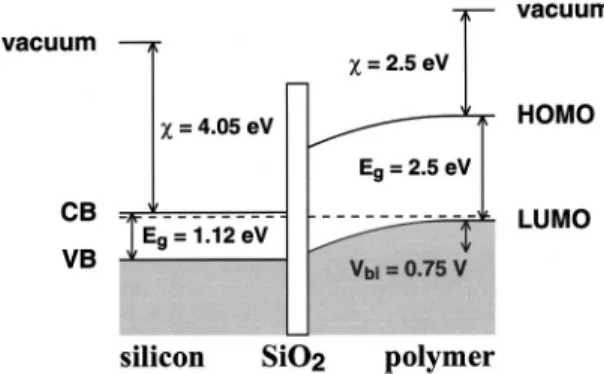
function only 4.3 eV兲, but to form ohmic contacts with, for instance, gold 共with a work function of 5.1 eV兲. With the latter, an accumulated region is formed with an increased density of free carriers at the interface. When the polymer is deposited on top of heavily doped n-type silicon 关electron affinity: 4.05 eV, band gap 1.15 eV共Ref. 15兲兴 the behavior is expected to be very similar to the aluminum–polymer inter-face with a built-in voltage of⬃0.75 V 共calculated from the difference in Fermi level positions in the silicon and poly-mer, which are expected to be close, say 0.1 eV, to the con-duction band and valence band, respectively兲.
The formation of a thin, insulating oxide on top of the silicon is unavoidable when, as in our case, the deposition is done at ambient conditions. This results in so-called metal– insulator–semiconductor 共MIS兲 tunnel diodes as described by Card and Rhoderick.16 The combined expected structure of the device is shown in Fig. 1.
The presence of an interfacial layer provides an extra degree of freedom to the energy diagram; a voltage drop in the insulating layer allows a shift of the band structure of the metal relative to the semiconductor. Also interface states
共caused by impurities or discontinuities at the interface兲 can
have a pronounced effect on the device; charged interface states can cause a voltage drop across the interface which can produce effects similar to a difference in work function of the two joined materials, also, a large number of interface states can pin the Fermi level at a certain energy. They can thus, for instance, force the interface to be inverted共an abun-dance of minority-carriers兲 and make the minority current dominate over the majority-carrier current.
When a device is inverted at zero bias the minority-carrier current will be a substantial fraction of the total cur-rent at small biases. When the voltage is increased, this ratio eventually drops.17,18 The minority-carrier current will de-crease 共or grow less rapidly兲, while the majority-carrier cur-rent continues to increase. The net effect is the formation of a plateau of reduced voltage dependence of the current in the forward bias I – V 共current–voltage兲 curve until the minority-carrier current has died out and the device has become majority-carrier type. This plateau can cause the device to have inverted rectification over a certain voltage range; the reverse-bias current can be larger than the forward-bias cur-rent.
III. EXPERIMENT
The films of MEH-PPV共1m thick兲 were deposited by spin coating onto n⫹silicon substrates with a bulk resistivity of 0.1 ⍀ cm. Prior to deposition, the silicon substrates were cleansed with diluted HF to remove any residual oxide layer and were rinsed several times in ultrapure water. Before the spin coating, the samples have been very briefly exposed to air and we estimate that this has caused an oxide layer on the silicon with a thickness of the order of 30 Å. After spin coating the films were immediately loaded into a turbo-pumped evaporator and gold was evaporated through a mask to form an array of circular electrodes 共2 mm in diameter兲. For the measurements the devices were mounted in a tem-perature controlled sample holder located inside a steel chamber evacuated to less than 10⫺5mbar. Small-signal ad-mittance measurements over the range 50 Hz–1 MHz were carried out with a Fluke PM 6306 RCL meter. The dc I – V curves were recorded with a Keithley 487 picoammeter/ voltage source. The sample temperature was varied in the range 100–300 K and measured with a chromel-alumel ther-mocouple placed on the substrate close to the devices. All the measurements were carried out in the dark. From the fabrication process until the characterization, the samples have been in ambient 共albeit dark兲 environments for some days. Prior to the measurements discussed here, the sample has undergone a heat treatment at 115 °C in vacuum.
IV. CURRENT–VOLTAGE MEASUREMENTS
Figure 2 shows a typical I – V curve of the MEH-PPV/ n⫹-silicon structure. The original scan, as taken freshly after mounting the sample into vacuum, shows some interesting features. The first thing to note is that the current densities are very high; the current is not much limited by the oxide layer. Second, the rectification ratio is very poor, only a fac-tor 16 is achieved between the reverse and the forward cur-rent at 兩1 V兩. Furthermore, the reverse current saturates, as predicted by thermionic emission theory共Bethe, see Sze for a comprehensive summary of dc conductance theories15兲. Fi-nally, in the forward current there is a large plateau from 0 to 0.3–0.4 eV V, as described in Sec. II. For small voltages, the I – V characteristic is even inverted. This I – V plot very much resembles the minority-carrier-MIS-tunnel diodes as FIG. 1. Expected energy diagram of an n-type silicon/PPV device with a
thin insulating layer共over which no voltage drop occurs兲. On basis of the electron affinities and band gaps of silicon共Ref. 15兲 and PPV 共Ref. 14兲, a rectifying contact is expected with a built-in voltage of 0.75 V.
FIG. 2. Typical I – V curves at 300 K after freshly mounting the sample from air into vacuum共dashed line兲 and after two weeks in vacuum 共solid curve兲. The I – V rectification ratio which was initialy very low increases to over 1000. Also, the plateau in the forward current, that is indicative for a substantial minority-carrier current, is removed. The device has been con-verted from minority-carrier type to majority-carrier type.
described by Green and Shewchun19and can be described in the following way: the MEH-PPV surface is in inversion under reverse and small forward biases. 共This inversion might be caused by the presence of interface states which can pin the Fermi level in the top half of the band gap at the interface as described in the previous section.兲 As the bias is increased the device goes from inversion to depletion and eventually to accumulation. In inversion, the major compo-nent of the current is the flow of electrons from the silicon to the conduction band of the polymer. When the voltage is increased, the ratio minority-carrier current to majority car-rier current eventually drops.17,18
Figure 2 also shows the I – V characteristics after placing the device two weeks in vacuum. The rectification ratio at
⫾1 V has soared to 2800 and the plateau in the forward
current has nearly disappeared. The device behaves like a normal diode now, namely a device of nonequilibrium majority-carrier type. Since the silicon-oxide layer is stable under these conditions, the interface states must have changed or have been removed by the persistent pumping. This would then remove the voltage drop or the Fermi level pinning and therefore the inversion layer.
V. AC CHARACTERISTICS
Studies of the capacitance (C) and the conductance (G) associated with the depletion region can provide additional information about the concentration and characteristics of electrically active centers. For that reason we also monitored the ac properties of the device. In standard theory of single-barrier devices the depletion layer capacitance follows20
C⫽A
冑
er0NA 2共V⫺Vbi兲, 共1兲
with NA the acceptor concentration, Vbithe built-in voltage,
A the area of the interface,rthe relative permittivity,0the
permittivity of vacuum, and e the elementary charge.21 Be-cause in these measurements a small ac voltage is superim-posed on the dc bias, the ac conductance, also sometimes called the dynamic conductance, will be equal to the deriva-tive of the DC current and therefore depends exponentially on the voltage. Both the capacitance and conductance in this simple model are independent of the ac frequency.
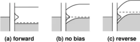
Interface states and deep levels can change the capaci-tance and conduccapaci-tance and can give rise to frequency depen-dencies as described by Nicollian and Goetzberger.22Figure 3 clarifies this idea for the interface states. For forward bi-ases the interface states are completely empty共that is neutral in the case of acceptor states兲, while for strong reverse biases they are completely full. In either case, modulating the Fermi level with the external voltage does not result in changes in the amount of charge stored on the interface states. For cer-tain biases the Fermi level can be degenerate with the interface-state levels 共middle plot in Fig. 3兲. Modulating it with the ac voltage results in charge flowing in and out of the interface states. This current is then proportional to the de-rivative of the ac voltage and is visible as an extra capaci-tance added to the capacicapaci-tance of Eq.共1兲 at certain voltages. Because energy can be lost in the process of transferring the
charge, some of the associated current is in phase with the ac voltage and is therefore visible in a contribution to the con-ductance.
For low frequencies the charges can follow the Fermi level modulation without problem. For high frequencies the trapping and detrapping times are much longer than the ac period and the interface levels cannot reach thermal equilib-rium. In that case the capacitance and conductance reduce to the depletion region values mentioned at the beginning of this section. Note that there is no dc contribution to the con-ductance since the number of interface states is finite; the conductance drops to zero at low frequencies, whereas the capacitance levels off共since the latter is calculated by divid-ing the out-of-phase current by the ac frequency, I90°
⫽C – Vac, where I0°⫽G – Vacdefines G). There is a
maxi-mum response in the G – V plot when the共radial兲 modulation frequency reaches the reciprocal trap filling time, ⫽1/. For very slow states this can be in the range of the dc scan-ning speed.
For states that do not respond to the ac signal, but still respond to the bias changes complicated effects take place. This is equivalent to the case of deep, nonresponding bulk states which will be discussed in the next section. States that do not even respond to the bias changes can still influence the C – V and G – V plot: fixed charges can cause a constant voltage drop and a rigid shift of the C – V and G – V plots along the voltage axis.22
To summarize, for MIS tunnel diodes with interface states it has been predicted that there is a peak in the C – V and G – V plots, with an intensity depending on the ac fre-quency and a voltage position depending on the distribution of the interface states in the forbidden gap.
Compared to interface states, deep levels that are homo-geneously distributed in space have very similar behavior but show themselves in the C – V plots stepwise, up-to a certain voltage, rather than as a peak as shown above. This will be discussed later, in the section on Mott–Schottky plots.
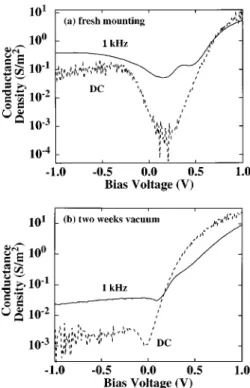
Figure 4 presents the G – V data. The freshly mounted sample shows a peak at 0.4 V forward bias at 1 kHz when corrected for the exponential dc conductances. We attribute this to interface states, as previously described.
The same sample placed in vacuum for longer periods has a much less pronounced peak in G – V, most of the in-terface states have been removed or changed by the pump-FIG. 3. Schematic band diagram of an MIS diode with interface states.共a兲 For forward biases, the Fermi level共dashed line兲 lies completely below the interface states which are therefore completely empty 共neutral兲. 共b兲 For some biases the Fermi level is resonant with the interface-state levels. In this case, a small change in the bias voltage results in charge flowing in or out of the interface. This is visible as an increased conductance and capacitance. 共c兲 For strong reverse biases the levels are completely occupied and there is no current upon changes in bias.
ing. This is consistent with the dc data as presented in the previous section.
Figure 5 summarizes the frequency dependence of the peak in the loss (G/). This was measured in another sample where the dc conductance was much lower共see inset兲 and the peak more pronounced. The figure shows that the largest response is for the lowest frequencies. Apparently, the maximum peak height in the G – V plot would occur for frequencies well below our measurement window共100 Hz–1 MHz兲, which indicates that the interface states are rather deep and the filling time is even longer than the 2 ms corre-sponding to 100 Hz. The shift of the peak towards lower
voltages for decreasing frequencies is caused by the ability to probe deeper states with longer relaxation times as the ac frequency is reduced. For higher frequencies the peak height in G/reaches a constant value, and a well at 0.1 V forward bias sets in. Both these effects, the leveling off of the peak height and a well rather than a peak, cannot be explained with the above theory. We will show what the cause is for the well.
Summarizing, the peak in G – V data correlates very well with the features seen in the I – V curves, and can be ad-equately described in the model of interface states that can be altered with persistent pumping. Apparently, the interface quality is both visible in the dc measurements as well as in the ac data.
VI. MOTT–SCHOTTKY PLOTS
It is common to present the capacitance–voltage data in so-called Mott–Schottky共MS兲 plots, 1/C2vs voltage (V). In ordinary situations, the slope in such a plot reveals the ac-ceptor concentration NA because, according to Eq.共1兲
d dV 1 C2⫽ 2 A2er0NA . 共2兲
This is applicable to the case of a single shallow acceptor共all ionized everywhere; space charge density in the depletion zone equal to the acceptor concentration兲, in which case the Mott–Schottky plot consists of a straight line pointing to Vbi
at the voltage axis when the concentration is uniform, or the slope represents the local acceptor concentration in case of nonuniform distributions. It is quite common to determine the acceptor concentration from the Mott–Schottky plots of single-level systems.
When there are more levels in the forbidden gap the situation becomes more complex 共see Fig. 6兲. First consider the situation of two acceptor levels, one shallow (EA
1 with
concentration NA1) and one deep (EA2 with concentration
NA2), in fact so deep that in the absence of bias it nowhere
drops below the Fermi level. This implies that all of the deep acceptor levels are filled共with holes兲 and are therefore neu-tral and do not contribute to the space charge and capaci-tance; the slope in the Mott–Schottky plot then represents only the shallow acceptor concentration. For strong reverse biases the increased band bending can force the deep accep-tor below the Fermi level at a region close to the interface. Now if the level is shallow enough so that it can respond to the ac probing signal 共of the order of 1 kHz兲 it will start contributing to the capacitance. The apparent concentration is then the sum of the two concentrations of the acceptors. This is visible in a sudden drop and a reduction of the slope to 1/(NA1⫹NA2) for biases smaller 共more reverse兲 than
Vbi⫺(EF⫺EA2),23,24as is easily seen in Fig. 6. Also, note
that the apparent built-in voltage seems to decrease; the in-tersect of the slope with the voltage axis is lowered to Vbi
⫺NA2(EF⫺EA2)/(NA1⫹NA2).
If the level is too deep and the probing frequency is too high compared to the characteristic level filling and empty-ing times, it does not respond anymore. It is still visible in
FIG. 4. 共a兲 Conductance density 共1/AR) plot at room temperature for the freshly mounted sample at 1 kHz 共solid兲. When the dc peak 共dashed兲 is subtracted from it, a positive peak at⬃0.4 V remains. 共b兲 After pumping for several weeks the peak is reduced, indicating the removal of the interface states. The dc conductance is calculated from the derivative of the I – V curves of Fig. 2.
FIG. 5. Frequency dependence of the loss共1/R) at room temperature for a sample with low conductivity共see inset兲. The low background conductance enables the observation of a peak in forward bias which is attributed to interface states. The largest response of the interface states occurs at the lowest frequency共200 Hz兲 and slowly decreases for higher frequencies 共500 Hz, 1 kHz, 2 kHz兲. After 3 kHz it levels off.
a reduction in the slope in the Mott–Schottky plot, but now without the sudden drop.23 It is important to note that the slope is no longer linear and a straight-line fitting does not reveal the true acceptor concentration anymore; Eq.共2兲 is no longer valid. Also, any extrapolation of the local slope to 1/ C2⫽0 increases to beyond Vbi.
If the second level is not a majority trap 共in this case acceptor level兲, but instead a minority trap, the situation is again a little different. Instead of the majority共quasi兲 Fermi level, EF p, as above, we now have to consider the minority
共quasi兲 Fermi level, EFn. These two can substantially deviate
from each other; large numbers of electrons injected into the conduction band move EF
n up. The difference between the
two at the interface is actually equal to the bias. Whereas the Fermi level for holes is flat throughout the entire polymer, the Fermi level for electrons is flat in the depletion zone and from there linearly falls back to meet EFp⫽EFsomewhere in
the bulk of the polymer.15The exact movement of this Fermi level and its slope in the bulk, and hence the intersect with the donor level, depend on parameters such as the injection ratio, the mobility of the electrons and the electron-hole re-combination rate. Therefore, it is not easy to calculate the precise effects of a minority level on the capacitance. When the donor level is completely above the 共minority兲 Fermi level everywhere, it is completely ionized and acts as com-pensation for the acceptors. The slope we see in the Mott– Schottky plot is then proportional to 1/(NA⫺ND). This is
especially the case for shallow donors. When the donor level
drops below the Fermi level somewhere, the effects become most complex. However, it is important to note that, as for all levels that are homogeneously distributed in space, the effects are visible stepwise in the voltage in contrast to cer-tain effects that have a voltage window.
Finally, for normal temperatures, the Fermi–Dirac dis-tributions over the levels make the effects smooth out a little. This is further enhanced by the use of finite ac amplitudes, in our case 50 mV. A sudden step in the capacitance, for in-stance, is in reality visible as a more gradual step. Also, interface states as described in the previous section can add structure to the Mott–Schottky plots.
With this information we can analyze the C – V data of the MEH-PPV. Figure 7 shows a typical Mott–Schottky
共MS兲 plot taken at an ac frequency of 100 Hz. It shows a
linear slope at reverse bias changing to a steeper slope at forward bias. Such plots with a sudden change in slope are often encountered in semiconducting polymers, see for ex-ample Refs. 25 and 26, and can be described well with the above theory. In the same figure, a simulation is shown in-cluding two levels, a shallow level with a concentration of 4.3⫻1015 cm⫺3 and a deep 共nonresponding兲 level 0.75 eV above the Fermi level with a concentration of 6.7⫻1016 cm⫺3. The extrapolation of the forward bias slope to the voltage axis reveals a built-in voltage of 0.75 V. This value is in agreement with the predicted value on the basis of the band-structure data共see Sec. II兲. The idea might occur to the reader that the change in slope in the MS plots instead is due to a spatial change in impurity concentration. In this case, the reverse-bias slope would indicate a sudden increase of the acceptor concentration from 4.3⫻1015 to 1.3⫻1016 cm⫺3as we move away from the interface. It is, however, unlikely that for different devices with different impurity concentra-tions the change in slope should always occur at the same voltage, as it does. Different sample preparations resulting in different impurity densities would cause a wide range of the FIG. 6. Schematic energy diagram for a system with two acceptor levels and
one donor level at forward bias. At a certain place the band bending is large enough to force the deep acceptor level below the共hole兲 Fermi level and it starts contributing to the space charge and capacitance. Closer to the inter-face the共electron兲 Fermi level crosses a donor level which now stops to compensate the acceptors and increases the space charge density. The ar-rows indicate the movement of the boundary edges upon an increase of the 共forward兲 bias.
FIG. 7. Typical Mott–Schottky plot共1/C2 vs V) measured at 100 Hz at room temperature共modulation depth: 50 mV, voltage step: 20 mV per sec-ond兲. The dots show the experimetal data, while the solid line represents a simulation with two acceptor levels. The shallow one is responding to the ac signal and has a concentration of 4.3⫻1015cm⫺3, while the deep one共0.75 eV above the Fermi level兲 is not responding and has a concentration of 6.7⫻1016cm⫺3. An⑀
r⫽5 was assumed.
sizes of the depletion width共at the same voltage兲 and hence a wide range of voltages where the edge of the depletion zone hits the boundary of the higher-doped region. On the other hand, in the above theory, the position of the change in slope is determined by the energetic positions of the levels in the gap, something that is expected to be independent of doping details.
For the freshly mounted sample, a much reduced slope was found compared to the pumped sample. This can be caused by a higher acceptor concentration, or, alternatively, by an increased absorption of the voltage drop by the inter-face layer. Again this would hint at an alteration of the in-terface by the persistent pumping.
In Fig. 8 the frequency dependence of the MS plots is shown. At frequencies above 200 Hz a structure appears at the small-bias range which again disappears at higher fre-quencies. This anomalous structure cannot be explained by the above theory of deep levels; a responding level could cause a positive slope in the MS plots, but would obviously also be visible at the lowest frequencies. Moreover, in a simulation the reverse-bias branch would drop far below the experimental data. On the other hand, a nonresponding deep level does not show itself as a peak in the MS plots共but is visible as a reduction in slope up to a certain voltage兲, nor does it have peaked response in frequency. In conclusion, the incorporation of deep levels into the model seems to predict the low-frequency data, but fails to explain the anomaly in the region of small bias for intermediate frequencies.
Similar anomalous structures in Mott–Schottky 共MS兲 plots have often been reported in the literature 共for instance for heterojunctions such as CuInSe2/CdS27兲, and are there explained in terms of共a兲 back-rectifying contacts, 共b兲 instru-mental artifacts,共c兲 deep levels,28共d兲 inductive effects due to minority carriers.18 In principle, a rectifying back contact could produce a local minimum in the C – V data by combin-ing the voltage dependencies of the capacitances of the two Schottky-barrier interfaces. Since gold, our back contact, makes a good ohmic contact with MEH-PPV we do not
ex-pect any rectifying properties. Instrumental artifacts such as parasitic capacitance of the cables were carefully checked and none were found below 1 MHz. Such effects normally start dominating at high frequencies while the devices stud-ied still displayed normal capacitance in the high-frequency-measurement range. As described above, deep levels cannot explain the anomalous effect. The structure might be due to interface states, but then it would rather be expected to be most pronounced at the lowest frequencies, in contrast to the observed frequency dependence. We present an alternative explanation, namely the inductive effects of minority-carrier injection.18,29
The underlying physics have been well described by Misawa for pn junctions:29 In the bulk region of the semi-conductor the minority-carrier current is mostly caused by diffusion, whereas the majority-carrier current is caused by drift. They move under the influence of the electric field caused by the IR voltage drop in the bulk. Diffusion is a rather slow process and the current cannot follow the voltage changes instantaneously; the current starts lagging behind the voltage and a shift of the phase of the current relative to the voltage occurs. If the phase shift is large this effect can imi-tate negative capacitance 共equivalent to inductance兲 and negative resistance; in the measurements one can observe a reduced capacitance and increased conductance. It must be noted that this is not a true capacitance in the sense that the device can store charge共this is the definition of static capaci-tance兲, but is rather an as-measured capacitance caused by a phase shift of the ac current.
Green and Shewchun present the same idea of the minority-carrier effects upon the ac characteristics of the de-vice. They show how Schottky diodes can become inductive under moderate bias due to the presence of small concentra-tions of minority carriers.18They also note that, by increas-ing the frequency of the applied signal, the correspondincreas-ing minority-carrier disturbance can be readily attenuated and the capacitance curves approach those expected on the basis of a one-carrier model. Furthermore, they were able to model the effects with the help of equivalent circuits containing frequency- and voltage-dependent components. These equivalent circuits do not reveal so much of the underlying physics, though.
According to Misawa, the total impedance of the p-type semiconductor can be described by the sum of the three terms
Z⫽Zp
1⫹Zp2⫹Zp3. 共3兲
The first term is purely resistive and is what is expected from the normal conductivity of the interface, namely the deple-tion width divided by the conductivity of the material caused by majority carriers: Zp 1⫽ W eppp . 共4兲
The magnitude of the second term is proportional to the dif-fusion length of minority carriers divided by the majority-carrier conductivity Ln/eppp which is multiplied by the
fraction of the minority-carrier AC current of the total ac current at the interface, In/I. This is further multiplied by a
FIG. 8. Frequency dependence of the Mott–Schottky plots such as shown in Fig. 7 at room temperature. A peak appears at small biases for intermediate frequencies.
factor ⌽ containing the phase which depends on the fre-quency () and minority-carrier lifetime (n) and is 180 ° (⫺R兲 for approaching zero and turns to 90°共L, or ⫺C兲 for higher frequencies. In a phase diagram⌽ is always in the quadrant (⫺R, L兲 and there is a maximum inductance for
n⬇2: Zp 2⫽ Ln eppp In I ⫺1
冑
1⫹in . 共5兲The last term, Zp3 is more complex; for instance it also
de-pends on the ratio of injected-minority-carrier density to thermal-equilibrium-majority-carrier density, n/ pp. It also
has a more complicated phase factor, which can make the impedance lie in any quadrant in a phase diagram:
Zp3⫽ Ln eppp n pp
冉
Indc I 1 1⫹冑
1⫹in ⫺I dc I 1冑
1⫹in冊
, 共6兲 with Indc the minority-carrier dc current and Idc the total dc current.As is clear from Fig. 8, in our device the minority-carrier current must be a substantial fraction of the total current for small biases; making Zp2 and/or Zp3 large and disappearing
again at larger forward biases. This explains the peaked be-havior in the Mott–Schottky plots. Figure 9 shows the fre-quency dependence of the amplitude of the well in capaci-tance for a different sample. The maximum in induccapaci-tance occurs at around 3 kHz indicating a minority-carrier lifetime of 100s.
An accompanying resistance plot is shown in Fig. 10. In this plot, an exponential conductance has been fitted and
sub-tracted from the data. It shows a structure of a broad well, stretching about 0.5 V, and inside it a positive-resistance narrow peak of 0.1 V width. On the basis of the frequency dependence of the amplitudes 共see Fig. 11兲, we can assign the broad well to Zp2 and the narrow peak to Zp3.
Appar-ently there are voltage regimes that favor the Zp2 term
共al-ways negative resistance兲 and regimes that favor the Zp
3
term. This can happen because Zp3 depends, apart from the
relative minority-carrier current, like Zp2, also on the
rela-tive minority-carrier concentration. As shown above, Zp1
and Zp2 two terms can have different frequency dependence.
We conclude that the relatively large minority-carrier effects at small biases are responsible for the capacitance and con-ductance anomalies presented here.
One final thing to note is that although the above theory gives an adequate explanation for the effects seen in our samples, we cannot completely rule out the possibility that they are related to the silicon surface and not to the intrinsic properties of the polymer. Gold–silicon junctions, made as reference samples, sometimes show effects in the C – V plots that resemble the ones reported here.
VII. ADMITTANCE SPECTROSCOPY
In reality the device we are measuring does not only consist of the interfacial layer共depletion layer兲, but is part of a larger structure which also contains the bulk material. In most cases this is a nuisance—the bulk resistance and ca-pacitance can make the measured values deviate substan-tially from the interface values—but in some cases we can make use of this effect. Figure 12 shows the equivalent cir-cuit used to represent the total device. A small calculation can show that even when all components in the circuit are frequency independent, the measured capacitance and resis-tance of the total circuit depend on the probing frequency. Assuming that the bulk resistance and capacitance (Rb and
Cb兲 are much smaller than their depletion layer siblings (Rd
FIG. 9. Frequency dependence of the amplitude of the well in the C – V plots, extracted from plots such as shown in Fig. 8. The maximum at 3 kHz indicates a minority carrier lifetime of 100s.
FIG. 10. At the same voltage where the structure appears in the Mott– Schottky plots共see Fig. 8兲, there is a wide well (Zp2) and a narrow peak
(Zp3) in the ac resistance. To obtain the plot an exponential conductance
was subtracted from the data; measured at 1.2 kHz.
FIG. 11. Frequency dependence of the well (Zp2, bottom兲 in the
ac-resistance plots共see Fig. 10兲 is linear in this range, while the frequency dependence of the peak (Zp3, top兲 is more complex. This follows the theory
of Misawa共see Ref. 29兲 for minority-carrier effects.
and Cd), the measured capacitance and resistance are equal
to the depletion layer values at low frequencies, while for high frequencies they are equal to the bulk values. Some-where between is a turning frequency. This frequency is eas-ily found when the data are plotted in the form of a loss tangent (tan␦⫽1/RC). This plot will have a local maxi-mum at a radial frequency:30
max⫽
1
Rb
冑
Cb共Cb⫹Cd兲. 共7兲
Figure 13 shows an example of the loss tangent共measured at a temperature of 200 K兲 with a maximum around 60 kHz. Because the temperature dependencies of the capacitances are relatively insignificant, the position of the peak should have the same temperature dependence as the bulk resis-tance. Furthermore, when we assume that the bulk resistance is governed only by the activation energy共constant mobility and constant density of states in the valence band兲, the resis-tance will follow
Rb⬀ exp共⫺Ea/kT兲, 共8兲
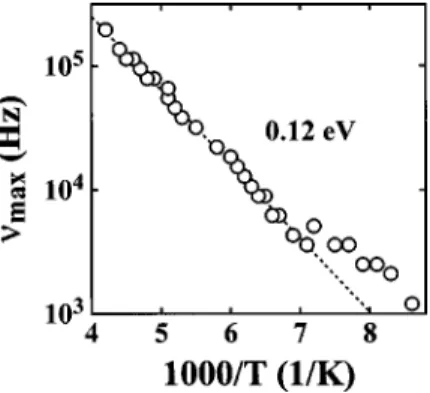
with Ea the bulk activation energy. Figure 14 shows the result. The Arrhenius plot of the position of the peak in the loss tangent of Fig. 13 versus ‘‘coldness’’ 共reciprocal tem-perature兲 shows a straight line, revealing an activation en-ergy of 0.12 eV.
The frequency at the maximum of the loss tangent has another important aspect. For all the ac measurements, we have to take care to always use frequencies below this turn-ing point in order to make sure that we are measurturn-ing the depletion layer properties. This is just an electronics effect and, apart from the trait described above, there is not much physics in it. For the classic semiconductors it is never a big
issue; normally for these materials the turning frequency is very high and we are always well below it. For polymers, especially those with high bulk resistivity, it can become a problem, though, and care has to be taken to choose suffi-ciently low frequencies in the measurements. The tradeoff of choosing low frequencies is that the noise increases rapidly
共so-called 1/f noise兲 and this sets the lower limit of usable
frequencies. For the samples under study, the cutoff fre-quency lies well above 100 kHz at room temperature and all the data represent the depletion region.
VIII. TEMPERATURE STIMULATED CURRENT
In a thermally stimulated current共TSC兲 experiment, the device is cooled down under strong forward bias. When the lowest temperature is reached the bias is removed and the sample is slowly warmed up while monitoring the current. In forward bias, the bands are flat and the deep acceptor level is nowhere below the Fermi level; they are all neutral. When the bias is removed the band bending is restored, but the temperature is too low to allow for emission of holes from the deep levels. When the temperature is slowly increased the holes will be reemitted at a certain temperature. The elec-tric field within the depletion layer will drift them towards the polymer-side electrode 共away from the interface兲 and a negative共reverse兲 current results. This is visible in the tem-perature stimulated current 共TSC兲 of Fig. 15. When all the
FIG. 12. Equivalent circuit used to model the admittance spectroscopy data. It consists of a loop representing the bulk共denoted by the subscript ‘‘b’’兲 in series with a loop representing the depletion layer共subscript ‘‘d’’兲.
FIG. 13. Example of a spectrum of the loss tangent共1/RC兲 at 200 K. A maximum occurs at 60 kHz.
FIG. 14. Arrhenius plot of the frequency position of the maximum in the loss tangent of Fig. 13 as a function of reciprocal temperature, revealing an activation energy EA⫽0.12 eV.
FIG. 15. Temperature stimulated current at 0 V bias共cooled down at ⫹1.0 V兲. The integration of the negative peak indicates a level with a concentra-tion of 4⫻1016cm⫺3.
holes have been emitted and the device has reached thermal equilibrium again, the current drops back to zero.
The number of holes emitted from the acceptors and contributing to the TSC can be found by integrating the peak: ⫺6.7 nC (4.2⫻1010 defects.兲 The depletion volume under the circular electrode is about 9⫻10⫺13 m⫺3 at 0 V bias 共based on a 300 nm depletion width and an electrode diameter of 2 mm兲 and 0 at strong forward bias. This gives an estimate for the concentration of the deep acceptor re-sponsible for the peak in Fig. 15; NA⫽4⫻1016 cm⫺3.
Whether this is correct, or the peak in TSC is due to interface states is not clear. The integrated current of⫺6.7 nC would correspond to an interface-state density of 1.3⫻1012cm⫺2, a reasonable number共for silicon surfaces15兲.
The same results can be obtained from a voltaic current transient. When the bias is suddenly removed, a small cur-rent lingers on. This is the curcur-rent that is related to the emp-tying共or filling兲 of deep levels which can take a long time to reach thermal equilibrium. The integrated current is also here equal to the number of deep impurities in the region that has fallen outside共or inside兲 the new depletion width. Figure 16 shows an example. Here the voltage was changed from ⫺1 to 0 V and the depletion width will have shrunk by about 75 nm. Hence, the integrated current of 2.5 nC indicates an acceptor density of⬃NA⫽6⫻1016cm⫺3. At the moment we
have no clear proof that these currents stem from bulk states or from inside the polymer. Future experiments will address this problem with the use of more advanced TSC and current-transient techniques.
Returning to the TSC measurements, the depth of the level can, in principle, be estimated when the position of the peak in TSC is determined as a function of the heating rate. For this to be accurate, the temperature scanning rate has to be very constant and well known over a long period of time. A much more direct and precise way to determine the level depth is via the temperature dependence of the loss tangent, as previously described, for the shallow level, or transient spectroscopy for the deeper levels. This will be described in Sec. IX.
IX. CAPACITANCE TRANSIENT SPECTROSCOPY
In this technique we observe the transient of the capaci-tance (C vs t) after a bias change. Levels are allowed to reach thermal equilibrium at a certain voltage. The transient is then recorded after switching the bias to a lower voltage. The charges that were originally trapped are emitted with a characteristic time, . The activation energy of the trap is calculated by noting that the emission rate, en⫽1/, of the
carriers from a trap of depth Ea at temperature T is given
by31
en⫽1/⬀T2exp共Ea/kT兲, 共9兲
where k is the Boltzmann constant. Measuring the time con-stant of the transients as a function of the temperature will then yield the trap depth, Ea.
The capacitance usually shows an immediate drop when the voltage is lowered, caused by the fast growth of the depletion region. The speed at which this happens is only
limited by the mobility of the majority carriers and is nor-mally too fast for the observation of a transient. This is then followed by a long-lived signal. For a majority-carrier trap we expect a negative capacitance transient 共upward trend兲; charges are released from the acceptors and the depletion width decreases, observable as a slowly increasing capaci-tance over time. For minority-carrier traps—traps that com-municate more readily with the minority-carrier band rather than with the majority-carrier band—the transients are ex-pected to be positive共downward trend兲;31upon a lowering of the bias the electron-Fermi level moves down and the elec-trons are released from the traps resulting in a decrease of the space charge density and hence an increase in the depletion width and a reduced capacitance. It is obvious that for a minority-carrier transient to be observed, minority carriers have be able to be injected into the polymer. To make sure of this, we made use of the heterojunction of heavily doped n-type silicon and the p-type polymer.
In standard deep-level-transient-spectroscopy 共DLTS兲 methods the device is primed many times per second. This is possible because for the classic materials such as silicon the decay times of the transients lie well below 1 s for all tem-peratures. The procedure is to take many transients per sec-ond and average them. To reduce the amount of calculation required, from these data only two data points at a fixed moment in time are kept 共the so-called time window兲. Re-cently, in Laplace DLTS, all data are taken into the calcula-tion 共made possible by the availability of cheap data-manipulating power in modern computers兲, and a larger sensitivity and resolution is obtained. For the polymers, the transients are much slower. Each transient is in the order of 100 s. For such long scans, averaging is not possible unless the temperature stability is compromised. This also inhibits the use of time windows; the scarce amount of data necessi-tates the full use of the data. We fitted a limited number of exponentials, up to three, to all the data points in a scan. In the few cases where the number of exponentials to use in the fit was not evident from the scan or the fit quality was bad the data were rejected.
Figure 17 shows that, in our case, by an appropriate pulse scheme, it is possible to prime either the minority- or the majority-carrier trap levels. The majority-carrier traps
FIG. 16. Voltaic current transient obtained after switching the bias from ⫺1 to 0 V. The integrated current 共2.5 nC兲 corresponds to an acceptor density of approximately NA⫽6⫻10
16
cm⫺3.
can be detected using a filling pulse of zero bias, and minority-carrier traps are revealed by injecting electrons into the polymer in a forward-bias pulse of 1.0 V. A complication is that forward-injecting bias pulses, because of the collaps-ing of the depletion region, can also significantly perturb the occupation of interface states 共which are more homoge-neously distributed in energy and hence give nonexponential contributions to the capacitance transients兲, which is not de-sirable because our interest is to prime only discreet bulk traps. Therefore, during the experiments the sample was kept under zero bias and then subjected to a reverse step of⫺0.8 V. The corresponding transient capacitance under reverse bias was recorded at a series of stabilized temperatures to provide the time constants ().
Although we did not forward bias the pn junction, we observe both types of transient corresponding to majority-and minority-type behavior. This reversal in the sign of ca-pacitance change is illustrated in Fig. 18, where for a certain temperature both types of behavior are visible at the same time. The observation of minority-type transients suggests that electron diffusion from the n⫹ silicon is enough to fill minority traps in the polymer. This is consistent with the results of the ac measurements where we showed evidence for minority-carrier currents in the small-bias range.
Figure 19 summarizes the decay times found in the tran-sients as a function of temperature. The solid and open circles represent majority and minority traps, respectively. Equation 共9兲 was then fitted to these data points. There is
clear evidence for at least four trap levels, two minority ones
共activation energies: 0.48 and 1.3 eV兲 and two majority ones 共activation energies: 1.0 and 0.3 eV兲. The data points related
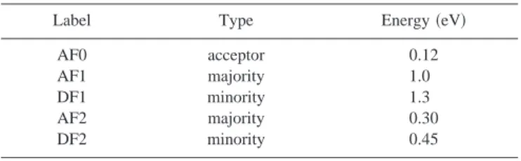
to these traps are so closely spaced that the exact determina-tion of the time constants is cumbersome and depends, for instance, on the fitting procedure. Hence, the activation en-ergy of the trap levels have a wide margin of error 共about 20%兲. It has to be noted however that there is no doubt of the existence of the above mentioned levels. Figure 20 and Table I summarize all the levels found in this work.
For another trap, one that is visible at room temperature and is not presented in Fig. 19, the temperature is stable enough to do a series of transients with different pulse lengths. The procedure is to have the device in reverse bias and remove the bias for a certain time , the pulse length. The amplitude of the transient as a function of the pulse length can reveal information about the type of the defect responsible for the transient.32,33For defects that can capture
FIG. 17. By a suitable choice of the pulse we can make the transients reveal a majority trap in a 0 to ⫺1.4 V pulse or a minority trap in a forward injecting pulse⫹1 to ⫺0.4 V. Measured at room temperature.
FIG. 18. At ⫺5 °C, three traps are visible in the same scan. A triple-exponential curve was fitted to it共dashed line兲. Measured at 1 kHz, 100 mV ac level, after a voltage step from 0 to⫺0.8 V.
FIG. 19. T2-corrected decay times as a function of coldness共reciprocal
temperature兲 for two runs. Solid circles denote majority-type transients, while open circles indicate minority-type trap levels. The area of each point is proportional to the transient amplitude (⫻5 in right plot兲. From these plots four trap level depths can be determined according to Eq.共9兲. They are summarized in Table I and Fig. 20.
FIG. 20. Graphical presentation of the levels found in this work placed in the forbidden gap of the MEH-PPV. The shallowest acceptor level, AF0, was found via the loss-tangent data共see the section on admittance spectros-copy兲, while the others were found via capacitance-transient spectroscopy; see Table I for the numerical details.
and emit single charges, the amplitude of the transient ⌬C follows:
⌬C共兲⫽⌬C⬁关1⫺exp共⫺兲兴, 共10兲
with the pulse length and a constant depending on the trap-filling time. This is the case for independent single do-nors or acceptors, when each trapping event is independent and has a certain fixed probability to occur. A plot of log关⌬C()⫺⌬C⬁兴 vs will be a straight line. For traps that can contain more than one charge, such as extended defects, or when the density of defects becomes so high that they feel each others Coulombic field, the probability of trapping a charge per unit time depends on the number already present; the trap filling time becomes increasingly longer. The above mentioned plot will no longer be a straight line because is not constant. Instead, the response is initially fast and be-comes slower and slower over time; the curve bends up-wards. In Fig. 21 the capacitance amplitude is plotted as a function of filling time. The conclusion is that the transient is caused by isolated defects.
X. SUMMARY
We have shown how we can get important information about the MEH-PPV from current and capacitance measure-ments, admittance spectroscopy, and transient spectroscopy. It has been shown how the ambient conditions can change the device from minority- to majority-carrier type. This is of importance for optical applications, since large minority-carrier injections greatly enhance the radiative efficiency of the device.
Furthermore, we have shown evidence for interface states in the conductance data 共see Figs. 4 and 5兲. These interface states seem to be alterable by persistent vacuum conditions.
Due to the combined effects of large minority-carrier currents at low voltages and the longevity of these electrons we see a pronounced structure in the C – V and G – V plots at small biases caused by a lagging behind of the minority-carrier current relative to the ac voltage as was already pre-dicted some decades ago for the classical semiconductors.
The capacitance transients were studied as a function of temperature and revealed four traps, two minority type traps and two majority type traps on top of the shallow level found by admittance spectroscopy and confirmed by the tempera-ture dependence of the dc current. The discrete natempera-ture of the levels indicate that they belong to bulk states, rather than interface states. For the latter we expect a continuous distri-bution of the levels in energy and this would be visible as nonexponential decay in the transients. In our case the choice of cathode-silicon, with a clean chemically inert surface probably caused a low amount of interface states on the polymer side, enabling the observation of true bulk states.
To determine the concentrations of the impurities, we made use of Mott–Schottky plots and the results were roughly confirmed in the TSC and voltaic-current-transient data.
We have shown how the theories and measurement tech-niques that were originally designed for the classical semi-conductors, such as Si and GaAs, can be applied to the new semiconductors of organic materials, such as MEH-PPV. Most of these materials have large band gaps and hence the possibility of very deep states. The relaxation times—the carrier emission and capture times from these deep states can be of the order of seconds up to hours. This places some measurement techniques, especially all the transient tech-niques, in a different time regime compared to classical semiconductors, although the underlying physics are the same.
ACKNOWLEDGMENTS
This work was supported by a TMR Grant, Contract No. FMRX-CT96-0083共DG 12 - BIUO兲. We would like to thank D. M. Taylor for valuable discussions and K. Petritsch for measuring the film thickness.
1
R. H. Friend, R. W. Gymer, A. B. Holmes, J. H. Burroughes, R. N. Marks, C. Taliani, D. D. C. Bradley, D. A. Dos Santos, J. L. Bre´das, M. Lo¨gd-lund, and W. R. Salaneck, Nature共London兲 397, 121 共1999兲.
2D. G. Lidzey, M. A. Pate, M. S. Weaver, T. A. Fisher, and D. D. C.
Bradley, Synth. Met. 82, 141共1996兲.
3
G. Yu, Synth. Met. 80, 143共1996兲.
4C. Zhang, H. von Seggern, K. Pakbaz, B. Kraabel, H. W. Schmidt, and A.
J. Heeger, Synth. Met. 62, 35共1994兲.
5Y. Fukada, T. Watanabe, T. Wakimoto, S. Miyaguchi, and M. Tsuchida,
Synth. Met.共submitted兲.
6
G. Yu, G. Srdanov, J. Wang, and A. J. Heeger, Synth. Met.共submitted兲.
7P. W. M. Blom, M. J. M. de Jong, and M. G. Munster, Phys. Rev. B 55,
656共1997兲.
8P. W. M. Blom, M. J. M. de Jong, and S. Breeddijk, Appl. Phys. Lett. 71,
930共1997兲.
9J. Birgerson, M. Fahlman, P. Bro¨ms, and W. R. Salaneck, Synth. Met. 80,
125共1996兲. TABLE I. Trap levels detected by transient spectroscopy and admittance
spectroscopy. See Fig. 20 for a graphical presentation of these levels.
Label Type Energy共eV兲
AF0 acceptor 0.12
AF1 majority 1.0
DF1 minority 1.3
AF2 majority 0.30
DF2 minority 0.45
FIG. 21. Pulse-length dependence of a majority-type transient at room tem-perature 共not visible in Fig. 19兲. The straight line indicates point defects rather than extended defects as the source of the transient.
10T. Osada, Th. Kugler, P. Bro¨ms, and W. R. Salaneck, Synth. Met. 96, 77
共1998兲.
11I. D. Parker and H. H. Kim, Appl. Phys. Lett. 64, 1774共1994兲. 12G. W. Jones, D. M. Taylor, and H. L. Gomes, Synth. Met. 85, 1341
共1997兲.
13
A. J. Campbell, D. D. C. Bradley, E. Werner, and W. Bru¨tting, Synth. Met.共submitted兲.
14F. Caciali, R. H. Friend, N. Haylett, R. Daik, W. J. Feast, D. A. dos
Santos, and J. L. Bre´das, Appl. Phys. Lett. 69, 3794共1996兲.
15S. M. Sze, in Physics of Semiconductor Devices, 2nd ed. 共Wiley, New
York, 1981兲.
16H. C. Card and E. H. Rhoderick, Solid-State Electron. 16, 365共1973兲. 17D. L. Scharfetter, Solid-State Electron. 8, 299共1965兲.
18M. A. Green and J. Shewchun, Solid-State Electron. 16, 1141共1973兲. 19M. A. Green and J. Shewchun, J. Appl. Phys. 46, 5185共1975兲. 20
P. Blood and J. W. Orton, Techniques of Physics 14: The Electrical Char-acterization of Semiconductors: Majority Carriers and Electron States
共Academic, New York, 1992兲.
21C. Caso et al., Eur. Phys. J. C3, 1共1998兲. 22
E. H. Nicollian and H. Goetzberger, Bell Syst. Tech. J. 46, 1055共1967兲.
23D. M. Taylor and H. L. Gomes, J. Phys. D 28, 2554共1995兲. 24I. Balberg, J. Appl. Phys. 58, 2603共1985兲.
25P. Stallinga, H. L. Gomes, G. W. Jones, and D. M. Taylor, Acta Phys. Pol.
A 94, 545共1998兲.
26
H. Antoniadis, B. R. Hsieh, M. A. Abkowitz, S. A. Jenekhe, and M. Stolka, Synth. Met. 62, 265共1994兲.
27J. Santamaria, G. Gonzales Diaz, E. Iborra, I. Martil, and F.
Sanchez-Quesada, J. Appl. Phys. 65, 3236共1989兲.
28
C. H. Champness and J. Pan, Can. J. Phys. 66, 168共1988兲.
29T. Misawa, J. Phys. Soc. Jpn. 12, 882共1957兲.
30H. L. Gomes, Ph.D. thesis, University of Wales, Bangor, 1993. 31D. V. Lang, J. Appl. Phys. 45, 3023共1974兲.
32E. F. Ferrari, M. Koehler, and I. A. Hu¨mmelgen, Phys. Rev. B 55, 9590
共1997兲.
33P. Omling, E. R. Weber, L. Montelius, H. Alexander, and J. Michel, Phys.
Rev. B 32, 6571共1985兲.