Brazilian Microwave and Optoelectronics Society-SBMO received 12 Dec 2017; for review 19 Dec 2017; accepted 26 Apr 2018
Brazilian Society of Electromagnetism-SBMag © 2018 SBMO/SBMag ISSN 2179-1074
All-Optical Logic Gates Devices based on
SPP Coupling between Graphene Sheets
Antônio Francisco Aguiar, Daniel Marchesi de C. Neves and João Batista R. Silva,
Depart. of Teleinformatics Engineering - DETI, Federal University of Ceara – UFC, Fortaleza, Ceará, Brazil (e-mail: [email protected], [email protected], [email protected])
Abstract—The aim of this work is to propose all-optical logic gates based on surface plasmon polaritons (SPP’s) coupling among spatially separated graphene sheets. This model consists of graphene nanoribbons embedded in silica (SiO2) substrate place in
a distance such that allow an efficient coupling between the plasmonic modes of the waveguides. It was numerically analyzed the propagation´s behavior of the SPP modes in an interferometric device as function of the chemical potential and geometrical parameters in order to obtain the AND/OR/XOR logic gates for OOK modulation.
Index Terms— Chemical Potential, Graphene SPP, Logic Gates, Nanophotonic devices
I. INTRODUCTION
Graphene properties have caused great interest and impact in the field of research that includes
advanced studies in optoelectronics and large in areas such as physics, chemistry, computation, biology and medicine. This new material showed more favorable characteristics such as extreme
electromagnetic confinement, loss level of dissipative losses and dynamic tunneling with change of chemical potential. These factors indicate greater flexibility than metal-based nanodevices,
characteristics that make them more favorable for photonic integration due to their small footprint [1]. This material still have a great potential of applications to be explored and has been undergoing
constant advances towards devices such as switching based on directional couplers, since electronic logic gates are a very important component in signal processing and transmission devices. However, the electronic logic gates have reached their in terms of miniaturization due the exponential increasing
of power consumption inversely with the device's size (Moore's law), which is related to some disadvantages in applications such as latency failures, that can lead to less security and reliability. One
way to overcome these limitations would be to use an all-optical architecture that drastically reduces port propagation and delays in state changes. An important advantage is seen when logic gates are
cascaded, where all ports can be changed simultaneously and delays do not cascade as in electronic logic gate, where the delays of their ports are cascaded. Innovations in fully optical devices come
Brazilian Microwave and Optoelectronics Society-SBMO received 12 Dec 2017; for review 19 Dec 2017; accepted 26 Apr 2018
Brazilian Society of Electromagnetism-SBMag © 2018 SBMO/SBMag ISSN 2179-1074 Varies all-optical logic gates have been demonstrated, one based on linear optical interferences [1, 3–8], and the other based on nonlinear optical effects [9–14]. While graphene-based optical logic gates we can highlight: 10 Gbps electro-optical logic gates using cascaded silicon graphene switches
based on MZI and 2 x 1 multimode interference combiners [2]; in [15] a type of optical logic device based on graphene surface plasmon polaritons (GSP) was proposed using the state of ‘‘ON/OFF’’ of
each input channel that it is controlled by changing the external gate voltage; in [16] it was reported the design procedure for developing subwavelength graphene-based plasmonic waveguide,
performing as a THz switch or an AND/OR logic gate; and in [17] it was introduced electro-optical MZI-based graphene plasmonic logic gates at the midinfrared. In all these proposed graphene-based
logical gates [2, 15-17], the modulating signal that defines states of ‘‘ON/OFF’’ is the voltage that is applied to the graphene layer.
Thus, inspired by the reported results in [18], this work proposes all-optical AND/OR/XOR logic gates devices based on SPP coupling between graphene sheets using to the graphene waveguide
splitter and keeping the applied voltage unaltered and using OOK modulation for each level the ON/OFF equivalent states. The paper is divided as follows: in Section 2, we made a brief introduction
to the fundamental issue of surface plasmon polaritons (SPP’s) coupling among spatially separated graphene sheets applied in a 1x2 interferometric device; for the Section 3, an 2x1 interferometric devices for realization of all-optical AND/OR/XOR logic gates based on SPP coupling between
graphene sheets was presented and investigated numerically; then, in the Section 4, we shown the conclusions and the perspective for future works.
II.
THEORYFrom a basic SPP coupling system, a graphene waveguide splitter, shown in Fig. 1, which was investigated in [18], the coupling coefficient of SPPs between the two graphene sheets can be written
as [17, 19]
.
2
gC
(1)
Where a good approximation for the propagation constant expression is given by
0
02 1
, 1
h g p p
SPP
p SPP p SPP
i k k u
k
u k k k d
(2)
considering that:
k
p
k
SPP2
hk
02
1 2,u
p
exp
k d
p
, [17]. h is a dielectric permittivity of mediumwhere the spatially separated double-layer graphene sheets are embedded, d is the separationdistance between the graphene layers, g is the graphene’s surface conductivity, 0 = 377 (air
impedance), k0 = 2/0 (0 is the incident light wavelength in air), kSPP = k0[h–4h2/(0g)2] is on the
Brazilian Microwave and Optoelectronics Society-SBMO received 12 Dec 2017; for review 19 Dec 2017; accepted 26 Apr 2018
Brazilian Society of Electromagnetism-SBMag © 2018 SBMO/SBMag ISSN 2179-1074 The optical propertie of a graphene monolayer is determined by the dynamic conductivity of the
graphene sheet (g), which is given by the Kubo´s formula [20], resulting in of the intraband´s
contribution, given by:
2
intra 2 1 ,
c ie i
(3)
and also to the interband contribution:
1 2 inter 1 2 ln , 4 2 c c i ie i
(4)
The (3) and (4) are valid under the condition kBT << |c|, where e is the elementary electron charge, c
is the chemical potential, ħ is the reduced Planck´s constant , is the radian angular frequency, is
the relaxation time constant, kB is the Boltzmann constant and T is the temperature in Kelvin [20].
The overall conductivity´s expression is given by the sum of interband and intraband contributions,
g() = intra + inter, where both parts determines which modes are allowed to propagate through the graphene’s waveguide and also determine the existence of TM or TE modes under these conditions: TM for μc > 0 and Im[σintra] > 0; and TE for Im[σinter]< 0 and |μc|< ћω/2 [21]. These properties allow us to control the conductivity and consequently can determine which SPP modes will be allowed to
propagate in a graphene nanoribbon according to which can be controlled with chemical doping through a gate voltage [20].
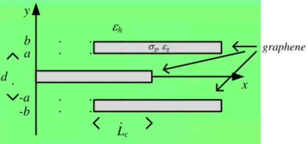
a -a -b b d Lc h
g, g graphene
y
x
Figure 1: The configuration of a graphene waveguide splitter 1x2 in 2D.
Subsequently, given the coupling coefficient in (1), one can determine the coupling length Lc,
which provides the distance traveled by the modes until a total transfer of energy from one waveguide to the other occurs, given by the equation [18, 22]:
. 2 2 C g L C
(5)
III.
ALL-OPTICAL GATESBrazilian Microwave and Optoelectronics Society-SBMO received 12 Dec 2017; for review 19 Dec 2017; accepted 26 Apr 2018
Brazilian Society of Electromagnetism-SBMag © 2018 SBMO/SBMag ISSN 2179-1074 2x1, as shown in Fig. 2.
The logic bit 0 and bit 1 were coded using an OOK modulation, i.e., when input port 1 (or input port 2 or both) is ON (insertion of light) bit 1 was transmitted on device to output, otherwise, when bit
0 is transmitted by one of the input ports, the input port is turned OFF (no radiation input).
In order to carry out a theoretical analysis, numerical simulations using the finite elements method
(FEM) in the frequency domain were performed for a dispersion analysis of propagation constants of the SPPs modes. In ours simulations, graphene was considered as a finite thickness material with
relative permittivity g = 1+ig0/(k0) [18]. In order to reduce the computational cost and, as a
consequence, providing a higher speed in the simulations, the graphene thickness was defined as =
1 nm. We can find in the literature GSPP devices which can operate on the C band´s range [2] as well as for 6 um [17, 20]. However, as shown in [20], in order to maintain the operation of this device at high doping levels, is necessary a considerably high electric field, which is not desirable. According
to the Kubo´s formula, there is an inverse relationship between the chemical potential in which the real conductivity (which is associated with the loss coefficient) drops considerably with the operation’s wavelength. Therefore, since for this device is required a low loss waveguide with the lowest chemical potential as possible, we choose the wavelength of 10 m which provides the optimal
ratio for mode confinement/losses and can operate in a relatively low chemical potential (below 0.25 eV) [20]. Furthermore, since we are working on terahertz regime, and the TE SPP modes are
supported only for up to mid-infrared frequencies (1.667 < ħω/μch < 2) with intrinsic losses
considerably (Im[σinter] < 0), for this device only the TM polarized SPPs modes are considered [20,
23].
Figure 2: Interferometric device with two inputs and one output.
The logic function OR can be obtained from the interferometric device shown in Fig. 2, with the
following configuration parameters: c = 0.229 eV, Lc = 294.46 nm, d = 50 nm, h = 2.1 (SiO2
dielectric medium). 0 = 10 m, T = 300 K and = 0.5 ps (is rather conservative to feature the
practical transport loss of graphene [18]). Figure 3 describes electrical field Ey and distribution of SPP
Brazilian Microwave and Optoelectronics Society-SBMO received 12 Dec 2017; for review 19 Dec 2017; accepted 26 Apr 2018
Brazilian Society of Electromagnetism-SBMag © 2018 SBMO/SBMag ISSN 2179-1074
Figure 3: Normalized Electric field Ey, and distribution of SPPs modes in a interferometric device as logic OR
gate with chemical potential of 0.229 eV,, Lc = 294.46 nm and d = 50 nm. Excitation input state (a) ‘10’, (b)
‘01’, and (c) ‘11’.
It is also possible to obtain the AND logic function with the same interferometric device, shown in
Fig. 2, only changing c, Lc and d to the following values, respectively,0.25 eV, 408.37 nm and 60
Brazilian Microwave and Optoelectronics Society-SBMO received 12 Dec 2017; for review 19 Dec 2017; accepted 26 Apr 2018
Brazilian Society of Electromagnetism-SBMag © 2018 SBMO/SBMag ISSN 2179-1074
Figure 4: Normalized Electric field Ey, and distribution of SPPs modes in a interferometric device as logic AND
gate with chemical potential of 0.25 eV,, Lc = 408.37 nm and d = 60 nm. Excitation input state (a) ‘10’, (b) ‘01’,
and (c) ‘11’.
The same interferometric device shown in Fig. 2 was also used to perform the XOR logic function
which makes use of destructive interference caused by an "S" shaped curve (two half circles with 50 nm radius of curvature, [24], placed on port 2, in Fig. 5. The size’s difference between graphene
Brazilian Microwave and Optoelectronics Society-SBMO received 12 Dec 2017; for review 19 Dec 2017; accepted 26 Apr 2018
Brazilian Society of Electromagnetism-SBMag © 2018 SBMO/SBMag ISSN 2179-1074
Figure 5: Normalized Electric field Ey, and distribution of SPPs modes in a interferometric device as logic XOR
gate with chemical potential of 0.212 eV, Lc = 346.75 nm and d = 50 nm. Excitation input state (a) ‘10’, (b) ‘01’,
and (c) ‘11’.
Table 1. Truth table and corresponding extinction (dB) for all-optical AND/OR/XOR graphene-based logic gates using OOK modulation.
Input OR (dB) AND (dB) XOR (dB) 0 0 0 - 0 - 0 -
0 1 1 -4.43 0 -11.30 1 -4.20
1 0 1 -4.43 0 -11.29 1 -4.75
1 1 1 1.46 1 -3.33 0 -24.23
In Table 1, we report our simulated extinction levels (which is the result of optical attenuation and the destructive’s interference processes) for all-optical AND/OR/XOR graphene-based logic gates using OOK modulation. At ON states (logic level 1), the extinction levels for all logics are at
Brazilian Microwave and Optoelectronics Society-SBMO received 12 Dec 2017; for review 19 Dec 2017; accepted 26 Apr 2018
Brazilian Society of Electromagnetism-SBMag © 2018 SBMO/SBMag ISSN 2179-1074 average extinction ratio between OFF/ON states of 6 dB for all types of logic. Therefore, a possible threshold value between “0” (OFF) and “1”(ON) results is -7 dB.
It was used to the power contrast ratio (PCR) to analyze the performance of the proposed logic gates. The PCR may be expressed (in dB) as PCR = 10log10 (P1∕P0), where P1 is power of logic ON at
the output channel and P0 is power of logic OFF at the output channel. It was found minimum PCR, approximately, 6 dB and 21 dB for AND and XOR logic gate, respectively.
IV. CONCLUSION
Based on the numerical simulations investigations carried out in this work, it can be concluded that
Nanophotonic devices based on graphene plasmonics (GSPP) are a very promising alternative in the design of logic gates devices with reduced footprint and power consumption. With this in mind, this
work was deepened in the study of propagation of SPP modes in waveguides, focusing on interferometric devices. The computational studies pointed to the feasibility of constructing all-optical
OR, AND and XOR logic gates, which were based on a graphene waveguide splitter (without changing the applied voltage to the graphene layer, defining the ‘‘ON/OFF’’ states) using OOK
modulation.
For the gate OR, the device showed higher transmission and coupling efficiency, around – 4 dB, for a chemical potential of 0.229 eV and although the graphene nanowires (sheets) were embedded in
silica substrate with relative electrical permittivity of 2.1, the results shown an efficient response in the implementation of this gate.
For the study of the AND gate, in order to obtain a constructive interference pattern, the transmission performance was reduced to a level around – 5 dB in the coupling region, when the two
input channels are ON, with c = 0.25 eV, Lc = 408.37 nm and d = 60 nm. It was also noticed that its
execution is less efficient than others, due to the small intensity distinction between the output values associate to bit 0 and 1.
Not least, the implementation of XOR gate has had a more significant change in geometry to
achieve the destructive interference pattern in the state in which the two input channels are ON. As mentioned before, in the fork shaped, there was added a "S" shaped path at input channel 2. This arrangement results in a destructive interference pattern in the case of two connected ports and
allowing the field to pass when only one of the input channels was configured for the ON state.
V. ACKNOWLEDGMENT
This work was financially supported by the Brazilian agencies FUNCAP, CAPES, CNPq via Grant
Brazilian Microwave and Optoelectronics Society-SBMO received 12 Dec 2017; for review 19 Dec 2017; accepted 26 Apr 2018
Brazilian Society of Electromagnetism-SBMag © 2018 SBMO/SBMag ISSN 2179-1074 REFERENCES
[1] Y.L. Fu, X.Y. Hu, C.C. Lu, S. Yue, H. Yang, Q.H. Gong, All-optical logic gates based on nanoscale plasmonic slot waveguides, Nano Lett. 12 (11) (2012) 5784–5790.
[2] Chen, W.; Yang, L.; Wang, P.; Zhang, Y.; Zhou, L.; Yang, T.; Wang, Y.; Yang, J. Electro-optical logic gates based on graphene–silicon waveguides. Opt. Commun. 2016, 372, 85–90.
[3] H. Wei, Z.X. Wang, X.R. Tian, M. Kall, H.X. Xu, Cascaded logic gates in nanophotonic plasmon networks, Nature Commun. 2 (387) (2011) 1–5.
[4] Y. Zhang, Y. Zhang, B. Li, Highly-efficient directional emission from photonic crystal waveguides for coupling of freely propagated terahertz waves into Si slab waveguides, Opt. Express 15 (15) (2007) 9281–9286.
[5] H. Wei, Z. Li, X. Tian, Z. Wang, F. Cong, N. Liu, S. Zhang, P. Nordlander, N.J. Halas, H. Xu, Quantum dot-based local field imaging reveals plasmon-based interferometric logic in silver nanowire networks, Nano Lett. 11 (2) (2011) 471–475.
[6] Y.L. Fu, X.Y. Hu, Q.H. Gong, Silicon photonic crystal all-optical logic gates, Phys. Lett. A 377 (3–4) (2013) 329–333.
[7] C.C. Lu, X.Y. Hu, Y. Song, Y.L. Fu, H. Yang, Q.H. Gong, Ferroelectric hybrid plasmonic waveguide for all-optical logic gate applications, Plasmonics 8 (2) (2013) 749–754.
[8] D. Pan, H. Wei, H. Xu, Optic interferometric logic gates based on metal slot waveguide network realizing whole fundamental logic operations, Opt. Express 21 (8) (2013) 9556–9562.
[9] V.R. Almeida, C.A. Barrios, R.R. Panepucci, M. Lip-son, All-optical control of light on a silicon chip, Nature 431 (7012) (2004) 1081–1084.
[10] Q. Xu, M. Lipson, All-optical logic based on silicon micro-ring resonators, Opt. Express 15 (3) (2007) 924–929.
[11] Z.H. Zhu, W.M. Ye, J.R. Ji, X.D. Yuan, C. Zen, High-contrast light-by-light switching and AND gate based on nonlinear photonic crystals, Opt. Express 14 (5) (2006) 1783–1788.
[12] Q. Liu, Z. Ouyang, C.J. Wu, C.P. Liu, J.C. Wang, All- optical half adder based on cross structures in two-dimensional photonic crystals, Opt. Express 16 (23) (2008) 18992–19000.
[13] M.W. McCutcheon, G.W. Rieger, J.F. Young, D. Da-lacu, P.J. Poole, R.L. Williams, All-optical conditional logic with a nonlinear photonic crystal nanocavity, Appl. Phys. Lett. 95 (22) (2009) 221102.
[14] Y. Liu, F. Qin, Z.-M. Meng, F. Zhou, Q.-H. Mao, Z.-Y. Li, All-optical logic gates based on two-dimensional low-refractive-index nonlinear photonic crystal, Opt. Express 19 (3) (2011) 1945–1953.
[15] Xiaoting Wu, Jinping Tian, Rongcao Yang, A type of all-optical logic gate based on graphene surface plasmon polaritons, In Optics Communications, Volume 403, 2017, Pages 185-192
[16] M. Yarahmadi, M.K.M. Farshi, L.L. Yousefi, Subwavelength graphene-based plasmonic THz switches and logic gates, IEEE Tran. THz Sci. Tech. 5 (5) (2015) 725– 731
[17] OOI, Kelvin J. A. et al. Electro-optical graphene plasmonic logic gates. Optical Society of America, (2014).
[18] WANG, Bing et al. Optical coupling of surface plasmons between graphene sheets, Applied Physics Letters 100, 131111 (2012). Solid State Communications, 150 pp. 1770 1773, (2010).
[19] M. L. Brongersma and P. Kik, Surface Plasmon Nanophotonics, (Springer, Dordrecht, 2007).
[20] OOI, Kelvin J. A. et al. Mid-infrared active graphene nanoribbon plasmonic waveguide devices, Soc. Am. B 30, 3111 (2013).
[21] S. A. Mikhailov and K. Ziegler, New electromagnetic mode in graphene, Phys. Rev. Lett. 99, 016803 (2007).
[22] WANG, Bing; WANG, Guo Ping. Surface plasmon polariton propagation in nanoscale metal gap waveguides, Optical Society of America, (2004).
[23] Kuzmin, D. A. et al. Transverse-electric plasmonic modes of cylindrical graphene-based waveguide at near-infrared and visible frequencies. Sci. Rep. 6, 26915; doi: 10.1038/srep26915 (2016).