Jorge Manuel Sousa Sales e Silva
Polaritons in Multilayer Semiconductor
Structures
Jorge Manuel sousa Sales e Silva
P olaritons inMultila y er Semiconductor Structures
Universidade do Minho
Escola de Ciências
Jorge Manuel Sousa Sales e Silva
Polaritons in Multilayer Semiconductor
Structures
Dissertação de Mestrado
em Física, ramo Física Aplicada
Trabalho efetuado sob a orientação do
Professor Doutor Mikhail I. Vasilevskiy
Universidade do Minho
Escola de Ciências
Polaritons in Multilayer Semiconductor
Structures
A
CKNOWLEDGEMENTSFirst and foremost, I would like to thank to the supervisor of this project, professor Mikhail I. Vasilevskiy, for his guidance and advice provided. His willingness to help and his involvement in this project had a huge impact on the final result.
I must also acknowledge the support and encouragement provided by my parents, Óscar and Maria, and my sister Sara.
A
BSTRACTThis work is dedicated to theoretical studies of plasmon- and phonon-based surface polaritons in layered materials using the transfer matrix method. For the study of surface plasmon-polaritons (SPPs), structures containing a single or a double interface between air and gold are considered. Surface phonon-polaritons (SPhPs) were investigated for two polar semiconductors, GaAs and GaN, for which the real part of the dielectric function is negative in the frequency range bewtween the transverse and longitudinal optical phonon frequencies. The similarities and differences between SPPs and SPhPs are discussed. For GaN, which is a uniaxial crystal, another type of proper mode is considered, named the guided mode, which can be observed (along with SPhPs) in the attenuated total reflection (ATR) configuration of far-infrared (FIR) spectroscopy.
A particular type of lossless interface mode called optical Tamm state (OTS), comprised between a polar semiconductor and a Bragg mirror is also investi-gated. The dispersion equation for OTSs is derived and calculated results are presented that show where and how OTSs are likely to be found on a GaAs/BR interface.
R
ESUMOEste trabalho é dedicado ao estudo de plasmões- e fonões-polaritões em mate-riais com várias camadas, através do método de transferência de matrizes. Para os plasmões-polaritões consideramos estruturas que contém interface simples e interface dupla ar-ouro-ar. No caso dos fonões-polaritões, investigamos dois semicondutores polares, GaAs e GaN, para os quais a parte real da função dielétrica é negativa no intervalo de frequências entre as frequências óptica transversal e óptica longitudinal. As diferenças e similaridades entre SPhPs são discutidas. No caso do GaN, existe um outro modo, chamado de modo guiado, que pode ser ob-servado segundo o método ATR (attenuated total reflection), que tem como base o processo de reflecção total interna.
Um tipo particular de modos é estudado, chamados de estados ópticos de Tamm (OTSs), entre o semicondutor polar GaAs e um reflector de Bragg. A re-lação de dispersão dos OTS é derivada e os cálculos presentes mostram o quão provável é a existência de tal estado na interface GaAs/reflector de Bragg.
C
ONTENTS✶✳ ■♥tr♦❞✉❝t✐♦♥ ✶
✷✳ ❊❧❡❝tr♦♠❛❣♥❡t✐❝ ✜❡❧❞s ✐♥ ❧❛②❡r❡❞ ♠❛t❡r✐❛❧s ✸
2.1. Maxwell’s equations and EM waves in vacuum . . . 3
2.1.1. Harmonic Fields . . . 4
2.1.2. Electromagnetic plane waves in vacuum . . . 4
2.2. Constitutive relations . . . 5
2.2.1. Complex permittivity and conductivity . . . 6
2.3. Maxwell’s Boundary Conditions . . . 7
2.4. Polarization of light at oblique incidence . . . 8
2.4.1. S-Polarization Fresnel coefficients . . . 10
2.4.2. P-Polarization Fresnel coefficients . . . 11
2.4.3. Reflectance and transmittance . . . 11
2.5. Surface waves and Attenuated Total Reflection (ATR) . . . 15
✸✳ ❙✉r❢❛❝❡ ♣❧❛s♠♦♥✲♣♦❧❛r✐t♦♥s ✭❙PPs✮ ✶✾ 3.1. Surface plasmon-polaritons at a metal/dielectric single interface . . . 19
3.1.1. Drude-Sommerfield theory for metal conductivity . . . 19
3.1.2. Excitation and propagation of SPPs . . . 20
3.2. Surface plasmon-polaritons in a dielectric/metal/dielectric double interface struc-ture . . . 25
3.2.1. Dispersion relation . . . 29
3.3. Concluding remarks . . . 31
✹✳ ❙✉r❢❛❝❡ ♣❤♦♥♦♥✲♣♦❧❛r✐t♦♥s ✭❙P❤Ps✮ ✸✺ 4.1. Surface phonon-polaritons at an air/GaAs single interface . . . 40
4.2. Surface phonon-polaritons in an air/GaAs/air double interface structure . . . . 41
4.3. Surface phonon-polaritons for a uniaxial crystal . . . 45
4.3.1. Optics of uniaxial media . . . 45
4.3.2. Surface phonon-polaritons at an air/GaN single interface . . . 46
4.3.3. Surface phonon-polaritons in an air/GaN/air double interface structure 50 4.3.4. Guided modes . . . 53
✺✳ ❚❛♠♠ ♣♦❧❛r✐t♦♥s ✺✼
5.1. Bragg reflectors . . . 57
5.2. Dispersion relation for Tamm polaritons . . . 66
5.3. Probing the Tamm States . . . 72
5.4. Concluding remarks . . . 76
✻✳ ❈♦♥❝❧✉s✐♦♥s ✼✼ ❆♣♣❡♥❞✐❝❡s ✽✸ ❆♣♣❡♥❞✐① ❆✳ P♦❧❛r✐③❛t✐♦♥ ♦❢ ❧✐❣❤t ❛t ♦❜❧✐q✉❡ ✐♥❝✐❞❡♥❝❡ ✽✸ A.1. S-polarization Fresnel coefficients . . . 83
A.2. P-polarization Fresnel coefficients . . . 84
L
IST OFF
IGURES2.1. Referential of a single interface between two dielectric media. . . 8
2.2. Scheme of oblique incidence of an EM wave propagating in two different di-electric media. . . 9
2.3. Schemes corresponding to (a) s-polarization and (b) p-polarization of light. . . 10
2.4. Reflectance for s-polarization and p-polarization, when ni< ntand ni> nT. . . 13
2.5. Transmittance of s-polarized and p-polarized electromagnetic waves for ni> nt. 14
2.6. ATR configuration. The yellow line corresponds to the surface polariton field while the brown one corresponds to the evanescent wave originated from the prism. . . 16 2.7. (a) Otto configuration and (b) Kretschmann configuration for the SPP excitation. 17 3.1. Plot of the real and imaginary parts of the Drude-type dielectric function for
gold, defined by the equation (3.34). The input parameters were ωp = 1.38 ∗
1016s−1= 9.10eV and Γ = 1.08 ∗ 1014s−1= 0.07eV. . . 21
3.2. Referential considered for the study of SPPs at an interface between air (ǫ1= 1)
and Gold, with a dielectric constant ǫ2(ω). . . . 23
3.3. Dispersion relation of SPPs at an interface between air and gold (Au). The damp-ing factor was neglected. The solid orange line corresponds to the dispersion curve corresponds to bound SPPs modes, where its propagation is allowed. The green solid line corresponds to the dispersion function of a EM wave in air. The dashed gray line corresponds to the plasma frequency of gold which is
ωsp = 9.10eV. The dashed black line corresponds to the maximum frequency
allowed for the propagation of the SPPs which is ωspp= 6.43eV (equation (3.25)). 24
3.4. Choice of axes (a) and geometry (b) of a gold film (of thickness d) cladded by
two semi-infinite dielectrics. We consider ǫ1= 1 and ǫ3= 1, which correspond
to air media. The frequency-dependent dielectric function ǫ2(ω) corresponds
to the Drude dielectric function of gold. Therefore we consider a structure of a finite gold layer cladded by two semi-infinite air media. . . 25 3.5. Dispersion curves for different gold layer thickness values, considering an air/gold/air
structure, Γ = 0. The black dashed line corresponds to the dispersion curve for a single air/Au interface. The gray dashed line is the maximum frequency allowed
for the propagation of SPPs, which corresponds to ωspp= 6.43eV. Solutions
3.6. Behavior of Ex(z) considering (a) an even mode (which corresponds to ω−mode)
and (b) an odd mode (which corresponds to ω+mode). Both modes values are
presented in table 3.1. The thickness considered is 50nm. Between z=0nm and z=50nm we observe two different behaviours, which is originated from the su-perposition of the SPP evanescent wave and the light wave. As expected, the
eletric field decays exponentially with the distance from the interfaces. . . 32
4.1. (a) Phonon dispersion curves for GaAs and (b) the first Brillouin zone of GaAs: the point Γ corresponds to the center of the Brillouin zone, i.e. [000], L repre-sents the wavevector direction [111] while X corresponds to the direction [010]. LO and TO are the longitudinal and transverse optical phonon modes, while LA and TA are the longitudinal and transverse acoustic phonon modes, respec-tively. Adapted from [12]. . . 37 4.2. Plot of the dielectric function defined in equation (4.18) with GaAs parameters.
The first plot (a) is for the case where damping is neglected, while in (b) are presented both the real and imaginary part of the dielectric function. The
pa-rameters used were ωLO= 36.58 meV, ωT O= 33.36 meV and ǫ∞= 10.89. . . 40
4.3. Dispersion curve for air/GaAs interface (a) for a wide interval of frequency val-ues and (b) for a more restrict frequency interval. In figure (a) the solid orange line corresponds to bulk and surface phonon-polaritons, the green solid line is the dielectric function in air, and the dashed lines show the reststrahlen band where SPhPs exist. In figure (b) the solid orange curve is the dispersion curve of the surface phonon-polaritons and the black dashed line corresponds to the
maximum frequency for the propagation of SPhPs, ωm = 36.30 meV. The
pa-rameters used are the same as in the dielectric function plot, figure 4.2a, where we set ΓT O= 0. . . 42
4.4. Dispersion curves for two different GaAs layer thickness values, considering an
air/GaAs/air structure. There is no damping considered, ΓT O = 0. The black
dashed line corresponds to the dispersion curve for a single air/GaAs interface.
4.5. Behavior of Ex(z) considering (a) an even mode and (b) an odd mode. Both
modes values are presented in table 4.3. The thickness considered is 5µm. Be-tween z= 0µm and z=5µm (GaAs medium) we observe two different behaviours, which is originated from the superposition of the SPhP evanescent wave and the light wave. As expected, the eletric field decays exponentially with the dis-tance from the interfaces. . . 44 4.6. Hyperbolic behaviour of the parallel and perpendicular dieletric function
com-ponents of GaN: (a) the real and imaginary parts of parallel component of the dielectric function (4.39), the vertical dashed line corresponds to the zero of the real part of the dielectric function, ω = 91.884 meV; (b) real and imaginary parts of perpendicular component of the dielectric function (4.40). The vertical dashed line also corresponds to the zero of the real part of the dielectric
func-tion, ω = 91.016 meV. The parameters used are shown in table 4.2. . . . 48
4.7. The orange curve corresponds to the surface phonon-polaritons’ dispersion curve of GaN, which stands to the right to the frequency values of light in vac-uum (green line). It was considered a air-GaN structure. The black dashed line
corresponds to the maximum frequency value ωmax= 88.046 meV. . . 49
4.8. Dispersion curve for a SPhP mode in a GaN layers of different thickness. There
is symmetry ǫ1= ǫ3= 1 and no damping is considered, Γ = 0. For a thick layer
the surface mode frequency is two-fold degenerate with respect to the two in-terfaces. For thinner films we observe that this degeneracy is lifted because of the interference of the two surface waves. The guided modes are studied in sec-tion 4.3.4. . . 51
4.9. Behavior of Ex(z) considering (a) an even mode and (b) an odd mode. Both
modes values are presented in table 4.3. The thickness considered is 3µm. Be-tween z= 0m and z=3µm (GaN medium) we observe two different behaviours, which is originated from the superposition of the SPhP evanescent wave and the light wave. As expected, the electric field decays exponentially with the dis-tance from each of the interfaces. . . 52 4.10.Dispersion plot for the first two guided modes considering an air/GaN/air
struc-ture. For higher wavevectors both modes tend to different frequency values. . . 54
4.11.Plot of Ex(z), in a GaN medium, corresponding to (a) the first guided mode ω =
4.12.Plot of the transmittance, reflectance and absorbance of a prism-air-GaN-air structure, regarding the frequency interval corresponding to the guided modes. Furthermore, there are many other guided modes propagating within the fre-quency interval [91.5456,91.7659] meV. The damping parameter was set to zero and therefore A(ω) = 0. These results are in agreement with those presented in [6]. . . 55 5.1. Schematics of a Bragg reflector structure considered in this work. A layers
cor-responds to Si, while the B layers correspond to Ge. The layers have equal
thick-ness. Cladding media 1 and are assumed as air. . . 58
5.2. (a) Reflectivity of the Bragg mirror (Si/Ge) localized between two semi-infinite air media; (b) Transmittance of the Si/Ge Bragg reflectors. The parameters used were ǫ1= ǫ2= 1, ǫA= 12 and ǫB= 16, d = 2.4µm, ΓT O= 0meV , θ =π4 and N = 30. 61
5.3. Reflectivity of the Bragg mirror multilayer structure (Si/Ge) for an angle of (a) 0 rad; (b)Π/6 rad; (c) Π/4 rad; (d)Π/3 rad. The other parameters used were
ǫ1= ǫ2= 1, ǫA= 12 and ǫB= 16, d = 2.4µm, ΓT O= 0meV and N = 30. . . . 62
5.4. Reflectivity of the Bragg mirror multilayer structure (Ge/Si) for different values of Si and Ge N layers: (a) 10 layers; (b) 20 layers; (c) 30 layers; and (d) 40 lay-ers.The other parameters used were ǫ1= ǫ2= 1, ǫA= 16 and ǫB= 12, d = 2.4µm,
ΓT O= 0meV and θ =π4. . . 63
5.5. Reflectivity of the Bragg mirror multilayer structure (Si/Ge) for different values of Si and Ge layers’ thickness: (a) d=1µm; (b)d=2 µm; (c) d=2.4 µm; d=3µ m and
(e) d=4µm. The other parameters used were ǫ1= ǫ2= 1, ǫA = 12 and ǫB = 16,
ΓT O= 0meV , θ =π4and N = 30. . . . 64
5.6. Bragg reflectors (Si/Ge) stop band frequency range for Si (or Ge) layer thickness of 2.3µm, 2.4µm and 2.5µm. The black dashed line correspond to the minimum and maximum frequency of the GaAs Restsrahlen band. The other parameters used were ǫ1= ǫ2= 1, ǫA= 12 and ǫB= 16„ ΓT O= 0meV , θ =π4 and N = 30. . . . 65
5.7. Schematics of a structure supporting OTSs. The vacuum gap of thickness δ (in reality it can be e.g. a polymer layer with a small refractive index n ≃ 1) can be considered as a microcavity. One of the heterostructures can be replaced by
another reflector (not Bragg), e.g. a metal or a polar semiconductor. . . 66
5.8. Two virtual interfaces (solid black lines) are introduced in the Ge uniform layer.
Both interfaces are separated by a phase Φ =n∆ω
c , where ∆ is the distance
5.9. Modulus and phase of a 10µm GaAs layer. The Reststrahlen band is localized between the dashed lines. . . 70
5.10.Eigenmode solutions for different angles of incidence. . . 70
5.11.Eigenmodes for different angles of incidence. . . 71 5.12.Schematics of coupling of a propagating EM wave (that is reflected at the
ex-ternal surface of the GaAs layer) to the optical Tamm state. The solid blue line
corresponds to the expected behaviour of the field profiles across the structure. 73
5.13.(a) Phase matching condition determining the frequency of a Tamm mode at
the interface between 1 µm GaAs layer and a BR with 200 periods, for θ =π
7, and
(b) the corresponding reflection spectrum. In the phase matching equation the
GaAs phonon damping was set equal to zero. . . 74
5.14.(a) Phase matching condition determining the frequency of a Tamm mode at
the interface between 5 µm GaAs layer and a BR with 200 periods, for θ =π
7, and
(b) the corresponding reflection spectrum. In the phase matching equation the
GaAs phonon damping was set equal to zero. . . 75
L
IST OFT
ABLES3.1. Values used to plot the eletric field Ex(z). . . . 32
4.1. Values used to plot the electric field Ex(z), figure 4.5. . . . 44
4.2. Values used to plot the parallel and perpendicular components of the dielectric function, figure 4.6. . . 48 4.3. Values used to plot the electric field Ex(z). . . . 52
1. I
NTRODUCTIONPolariton is a mixed quasiparticle formed by a photon and a crystal excitation, like, for ex-ample, phonons, plasmons or excitons. Polaritons can be formed in bulk crystals, at their surfaces, in quantum confined structures and microcavities [1]. Their characteristic feature is the strong coupling of an electromagnetic (EM) wave to the crystal excitation carrying an electric or magnetic dipole excitation. According to the type of this excitation one can distin-guish phonon-polaritons, plasmon-polaritons, exciton-polations, etc. The term "polariton" was proposed by J. Hopfield, [2], although the strong coupling between excitations and light in polar semiconductors had been considered earlier by K. B. Tolpygo [3], where the mixed quasiparticles were named "light-exciton". The exciton-polaritons are probably the most ex-tensively studied type of polaritons. Among their interesting properties is the experimentally observed Bose-Einstein condensation [1], due to the fact that it occurs at much higher tem-peratures than the same phenomenon in atomic vapors. Furthermore, a new type of laser, which is usually called polariton laser, has been demonstrated. Plasmon-polaritons, more specifically the surface plasmon-polaritons (SPPs), involve free electron oscillations instead of excitons. SPPs are evanescent EM waves coupled to the free electron plasma, propagating along the surface of a conductor. If the conductor is a metal with a typical free electron
con-centration of the order of 1022cm−3, the characteristic plasma frequency is the higher than
1016s−1, so these oscillations couple to the ultraviolet (UV) radiation. However, in doped
semiconductors the typical concentrations are much lower, usually below 1018cm−3, which
correspond to the far-infrared spectral range. SPPs can also be supported by doped graphene, the monolayer thick conductor which has been extensively studied in the last decade. The graphene SPPs also belong to the far-infrared or even the THz spectral range [4]. Conse-quently, they can also interact with optical phonons if the material is polar (i.e. is at least partly ionic), so eventually phonon-plasmon-polaritons can be formed [5].
The investigation of optical properties of materials in the infrared (IR) frequency range has been done for many years, through some well-known experimental techniques, such as Ra-man scattering and transmission and reflection spectroscopy. One of the strengths of these traditional IR spectroscopy techniques is the ability, as an analytical method, to obtain spec-tra from a very wide range of solids, liquids and gases. This technique is conducted with an infrared spectrometer in order to obtain the spectrum. The IR radiation region covers the wavelength range of 70nm−1nm, which correspond to frequencies 430THz−300 GHz and
photon energies of 1.24meV-1.7eV. It is usually divided into three sub-regions: the near-IR, which covers the photon energy interval of 1700 meV −500 meV, the mid-IR, which covers approximately 500 meV −50 meV, and the far-IR that goes from approximately 50 meV to 1meV. Recently, these were supplemented by new techniques in order to obtain additional information. One of these techniques, called attenuated total reflectance (ATR), consists on adding a prism coupler held a short distance away from the sample, with the purpose of ex-citing surface or guided modes.
In the present work, the objective was to consider theoretically several types of surface po-laritons. The following two chapters are devoted to fundamentals of electromagnetism in layered media and an example of surface EM waves coupled to metal plasmons. Phonon-based surface polaritons occuring in the FIR range due to the coupling of EM radiation to polar optical phonons are studied in chapter 4. This part of the thesis was inspired by the experimental and theoretical work [6]. Finally, a new type of interface mode, called Tamm polaritons, is investigated, with the results presented in chapter 5.1
1In this work, CGS unit system will be used. CGS units allow the unification of electricity and magnetism and optics, while SI system uses separate definitions for the vacuum permittivity and permeability, which implies that electric and magnetic fields are described by quantities of different dimension. In contrast, in the CGS units all four fields, E, D, B and H have the same dimension.
2. E
LECTROMAGNETIC FIELDS IN LAYERED MATERIALS2.1. MAXWELL’S EQUATIONS ANDEMWAVES IN VACUUM
The famous Maxwell’s equations govern the physics of electromagnetism and there are two important versions of them: Maxwell’s microscopic equations and Maxwell’s macroscopic equations. The first are more fundamental and were built taking into account that a field arises from a single electric charge and from their motion. However, the Maxwell’s macro-scopic equations explain the electromagnetism of macromacro-scopic media much more conve-niently than the microscopic ones:
∇ · D = 4πρext, (2.1) ∇ · B = 0, (2.2) ∇ × E = −1 c ∂B ∂t, (2.3) ∇ × H =4π c Jf+ 1 c ∂D ∂t, (2.4)
where E ≡ E(r,t) is the electric field, B ≡ B(r,t) denotes the magnetic induction, D ≡ D(r,t) corresponds to the electrical displacement field and H ≡ H(r,t) to the magnetic field inten-sity. These fields are related in the following way:
E = D − 4πP (2.5)
B = H + 4πM, (2.6)
where P ≡ P(r,t) and M ≡ M(r,t) the polarization and magnetization of the medium, respec-tively, which will be explained in more detail in subsection 2.2.
The sources of the EM field, ρext and Jf, correspond to the external charge density and free
current density, respectively. It is important to note that the external charge density corre-sponds to the the charge imbalance in the medium and does not include any charge
imbal-ance caused by external fields. The quantities ρext and Jf satisfy the continuity equation,
which expresses the conservation of charge:
∂ρext
∂t + ∇ · Jf = 0. (2.7)
Equation (2.1) tells us that free electric charges are the sources of electric displacement and equation (2.2) means that magnetic induction is source free. Both equations (2.3) and (2.4) show us how temporally varying electric and magnetic fields generate each other.
2.1.1. HARMONICFIELDS
Far from the source of the electric field (a charged particle), the electric field will behave like a plane wave. Consequently, these two fields can be defined as plane harmonic waves:
E(r, t ) = E0ei (k·r−w t), (2.8)
H(r, t ) = H0ei (k·r−w t), (2.9)
where E0and H0are constant vectors giving the amplitudes and direction of the fields, k is
the wave vector of the field and ω the angular frequency.
Both of these solutions describe arbitrary EM waves propagating through vacuum with light velocity c. The wave propagates in the wave momentum vector k direction. Both wave func-tions are orthogonal to the direction of propagation of the EM wave. Consequently, the am-plitudes of both waves are equal:
|E(r, t)| = |H(r, t)| (2.10)
The interest in evaluating the observable fields, brings the need to express the electric and magnetic fields as real harmonic fields:
E(r, t) = RehE0ei (k·r−w t)
i
= E0cos¡k · r − wt + φE¢ ; (2.11)
H(r, t) = H0cos¡k · r − wt + φH¢ , (2.12)
where φEand φHare the phases of the electric and magnetic fields, respectively.
2.1.2. ELECTROMAGNETIC PLANE WAVES IN VACUUM
In vaccum, both external charge density, ρext, and free current density Jf are equal to zero.
Consequently, we can obtain both electric and magnetic fields’ waves propagating in vacuum by applying the curl of a curl of a vector field A(which is either E or H):
Therefore, it is possible to obtain the eletric and magnetic fields equations by using Maxwell’s macroscopic equations (2.1), (2.2), (2.3) and (2.4):
∇2E(r, t ) − 1 c2 ∂2 ∂t2E(r, t ) = 0, (2.14) ∇2H(r, t ) − 1 c2 ∂2 ∂t2H(r, t ) = 0. (2.15) 2.2. CONSTITUTIVE RELATIONS
Although Maxwell’s equations define the fields that are generated by charges and currents, they do not describe how these charges and currents are generated. Therefore, Maxwell’s equations need to be supplemented by relations that describe the behavior of matter under the influence of fields. These are known as constitutive relations.
The response of the medium to an external electrical field (polarization), is not instantaneous but it arises after the field is applied. The most general linear dependence between D and E can be written as:
D(r, t) = ∞ Z −∞ ∞ Z −∞ ˜ǫ¡r − r′, t − t′¢ E¡r′, t′¢ dr′3dt′, (2.16)
where ǫ is the dielectric function. The statement which is being made here is that D at a given time t and position r, depends on the value of the electric field E at all positions r′and times t′. Thus, the material is both temporally and spatially dispersive. The latter is also known as a nonlocal medium. The relation (2.16) is a convolution in space and time. Thus, we can use the Fourier transform in order to obtain:
ˆ D¡kx,ky,kz,ω¢ = µ 1 2π ¶4 ∞Z −∞ ∞ Z −∞ ∞ Z −∞ ∞ Z −∞
D¡x, y, z, t¢ei kxxei kyyei kzzeiωtdxdydzdt, (2.17)
which allow us to rewrite equation (2.16) as ˆ
D(k,ω) = ǫ(k,ω) ˆE(k,ω), (2.18)
where ǫ is the Fourier transform of ˜ǫ. One of the reasons why it is most convenient to study in Fourier space is that a nonlocal relationship in space and time becomes an algebraic relation relation in (k,ω) space, only depends on the excitation at (k,ω) and not at¡k′,ω′¢. In order to
preserve causality, we must have ˜ǫ¡r − r′, t − t′¢ = 0 for all t′> t, i.e. there can be no response
Spatial dispersion is encountered near material surfaces or in objects whose size is compara-ble with the mean-free path of electrons. On the other hand, more frequently it is important to take temporal dispersion into account.
If nonlocal effects can be neglected we can rewrite relation (2.18) as ˆ
D(r,ω) = ǫ(r,ω) ˆE(r,ω), (2.19)
Similarly, for the magnetic field we have
ˆB(r,ω) = µ(r,ω) ˆH(r,ω), (2.20)
where µ(r,ω) corresponds to the magnetic permeability.
On a final note, it will also be mentioned the linear response of the electric field E to an
in-duced current Jf. This phenomena can be described by the following integral:
Jf(r, t) = ∞ Z −∞ ∞ Z −∞ ˜ σ¡r − r′, t − t′¢ E¡r′, t′¢ dr′3dt′, (2.21)
where ˜σ is the conductivity function. This means that the Jf at a given time t and position
r, depends on the value of the electric field E at all positions r′and times t′< t, in order to preserve causality.
Similarly to the relation (2.19), if nonlocal effects can be neglected we can express the linear
relation between E and Jf through
ˆJf(r,ω) = σ(r,ω) ˆE(r,ω). (2.22)
2.2.1. COMPLEX PERMITTIVITY AND CONDUCTIVITY
The induced current is related to the dielectric function ǫ(r, t) as we shall demonstrate. We can begin to define the complex dielectric function:
ˆǫ(ω) = ǫ′(ω) + iǫ′′(ω), (2.23)
where the term ǫ′(ω) is real, and ǫ′′(ω) is the imaginary part of the complex dielectric
func-tion. Both terms represent physical phenomena: the real part represents the energy accu-mulated in the dielectric medium while the complex dielectric function corresponds to the
dissipation or loss of energy in the medium. By working with equations (2.19) and (2.22), and by using Maxwell’s equations (2.3) and (2.4) one can determine the following expression:
∇ × H(ω) = −iω c · ˆǫ(ω) + i4π ˆσ(ω) ω ¸ E(ω) . (2.24)
Consequently, the complex permittivity function ǫ′′(ω) is related to the surface conductivity
in the following way:
ˆǫ(ω) = ǫ′(ω) + i4π ˆσ(ω)
ω . (2.25)
The response of a medium to harmonic fields at the high-frequency limit, ˆǫ′is usually referred
to as ǫ∞. At the plasma frequency and above, dielectrics behave as ideal conductor because
the imaginary part of the dielectric function vanishes, not existing energy dissipation.
2.3. MAXWELL’SBOUNDARYCONDITIONS
When an EM wave propagates from a medium to another medium with distinct properties, it can be transmitted or reflected at the surface. These properties of the transmitted and reflected EM waves come from Maxwell’s boundary conditions:
I SE · dA = 4πQf enc (2.26) I SH · dA = 0, (2.27) I LE · dl = − 1 c d d t Z SH · dA, (2.28) I LH · dl = 4π c If enc+ 1 c d d t Z SD · dA, (2.29)
where Qf enc is the free charge enclosed in a surface S, and If enc is the free charge current
enclosed by a loop L. As most of optical media are non-magnetic, we consider µ = 1 and therefore B = H.
Both D and H are generally discontinuous at a boundary between two different media. If we draw a cylinder and consider the equations (2.26) and (2.27), we can obtain the following boundary conditions:
D⊥1 − D⊥2 = 4πρf, (2.30)
� � �1, �1 � , � ෝ� ℎ
Figure 2.1: Referential of a single interface between two dielectric media.
where ρf ≡ ρf(r, t) is the free charge density on the surface of the interface. Now we have to
evaluate the components of D and H which are parallel with the interface plane. If we draw an Amperian loop between the two media, and imagine the situation where h −→ 0, we can deduce from equations (2.28) and (2.29) the following:
Ek2− Ek1= 0, (2.32)
Hk2− Hk1=
4π
c Jf × ˆn, (2.33)
where Jf ≡ J(r, t) is the surface free current density and ˆn is the versor perpendicular to the
interface.
2.4. POLARIZATION OF LIGHT AT OBLIQUE INCIDENCE
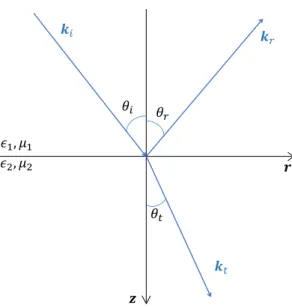
It is possible to use Maxwell’s boundary conditions to study oblique incidence of an EM wave through different dielectric media, see figure 2.2.
Considering that there is no free charge density ρf and free surface current density Jf, we
obtain the Maxwell’s boundary conditions for oblique incidence [7]: ǫ1¡(EI)z+ (ER)z¢ = ǫ2(ET)z
(EI)x,y+ (ER)x,y= (ET)x,y
µ1¡(HI)z+ (HR)z¢ = µ2(HT)z
¡(HI)x,y+ (HR)x,y¢ = (HT)x,y
When we consider oblique incidence we must take into account the contributions of the elec-tric and magnetic fields perpendicular and parallel to the interface surface between the two
�� �� �� � �∥ �� �1, �1 � , � �� ��
Figure 2.2: Scheme of oblique incidence of an EM wave propagating in two different dielectric media.
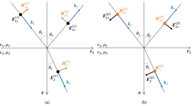
dielectric mediums. Thus, we must consider two different polarizations: s-polarization (or TE waves) and p-polarization (or TM waves), see figure 2.3.
An arbitrarily polarized plane wave, like the E wave equation (2.8), can be written as the su-perposition of two orthogonally polarized plane waves:
E = E(s)+ E(p), (2.34)
where E(s)and E(p)are plane waves perpendicular and parallel to the incidence plane
inter-face, respectively.
The reflection and transmission Fresnel coefficients are defined as [8]:
Er= ˆr(s)· Ei (2.35)
Hr= ˆr(p)· Hi (2.36)
and
Et= ˆt(s)· Ei. (2.37)
Ht= ˆt(p)· Hi, (2.38)
where ˆr(s)and ˆr(p)are the Fresnel reflection coefficients and ˆt(s)and ˆt(p)are the Fresnel trans-mission coefficients for s and p-polarization, respectively.
�� �� �� � �∥ �� �1, �1 � , � �1� � �1� �� �� � �1� �1� (a) �� �� �� � �∥ �� � , � � , � ��� ��� �� ��� ��� �� �� �� (b)
Figure 2.3: Schemes corresponding to (a) s-polarization and (b) p-polarization of light.
2.4.1. S-POLARIZATIONFRESNEL COEFFICIENTS
Using the coordinate system shown in figure 2.3a, we have:
E(s)i = ˆyEiei(ki·r−ωt) (2.39)
E(s)r = ˆyErei(kr·r−ωt) (2.40)
E(s)t = ˆyEtei(kt·r−ωt) (2.41)
The Fresnel coefficients for this polarization are the following [8]: ˆr(s)=µ2k1z− µ1k2z µ2k1z+ µ1k2z , (2.42) where k1z= s ǫ1ω 2 c2 − k 2 x and k2z= s ǫ2ω 2 c2 − k 2 x. and ˆt(s) = 2µ1k2z µ2k1z+ µ1k2z. (2.43)
2.4.2. P-POLARIZATIONFRESNEL COEFFICIENTS
For this type of polarization it is used the coordinate system presented in figure 2.3b. In this case the H field is parallel to the surface:
H(p)i = ˆyHiei(ki·r−ωt) (2.44)
H(p)r = ˆyHrei(kr·r−ωt) (2.45)
H(p)t = ˆyHtei(kt·r−ωt) (2.46)
The Fresnel coefficients for p-polarization are defined as [8]: ˆr(p)=ǫ2k1z− ǫ1k2z ǫ2k1z+ ǫ1k2z (2.47) and ˆt(p) = 2ǫ2k1z ǫ2k1z+ ǫ1k2z s µ2ǫ1 µ1ǫ2 (2.48)
The calculations required to obtain the coefficients expression are presented in Appendix
section A.2. Most optical media are non-magnetic, so µ1≈ µ2≈ 1 and
ˆt(p)
= 2ǫ2k1z
ǫ2k1z+ ǫ1k2z
r ǫ1
ǫ2. (2.49)
2.4.3. REFLECTANCE AND TRANSMITTANCE
When light propagating in a medium of refractive index n1incides on an interface separating
two different dielectric media it can be reflected or transmitted. Since the second medium has a different refractive index, light will behave differently. The electromagnetic wave will be attenuated if the refractive index of the second medium is higher. The change of behaviour of the electric and magnetic fields can be studied experimentally by measuring the intensity of the incident, reflected and transmitted EM waves. Consequently, it is possible to study the reflectance and transmittance of the EM wave. The time rate of flow of electromagnetic energy per unit is given by the Poynting vector:
S =4πc Re[E × H]. (2.50)
The magnitude of this vector is basically the wave velocity v multiplied by the time-average electromagnetic energy density 〈U〉:
|S| = v · 〈U 〉, (2.51) where 〈U 〉=4π1 Re ·1 2(E × H) ¸ =16π1 ¡E · E∗+ H · H∗¢ . (2.52)
In reality the optical field oscillates at 1015Hz and there is no detector capable of measuring the instantaneous energy flow. Consequently, what is measured is the time-average of the energy flow:
〈S〉 = Ik
k = I ˆn, (2.53)
where I is generally referred to as the intensity of the electromagnetic wave, which has units of power per unit area, and ˆn is the normal vector of the interface surface plane.
Due to diffraction, the beam size of the transmitted wave is different than the beam size of the incident wave. Reflectance of the surface of a material is its effectiveness in reflecting radiant energy. It is defined as the fraction of the incident EM wave intensity over the intensity of the reflected EM wave intensity:
R = IR
II
, (2.54)
where IIis the intensity of the incident wave and IRis the intensity of the reflected wave. On
the other hand the transmittance is defined as:
T =IT
II
, (2.55)
where IT the intensity of the transmitted wave. The reflectance for the transmittance and
reflectance of a s-polarized electromagnetic wave are equal to:
R =|Eyr| 2 |Eyi|2 , (2.56) T =µ1 µ2 |Ey t|2 |Eyi|2 |k2| |k1| cosθt cosθi . (2.57)
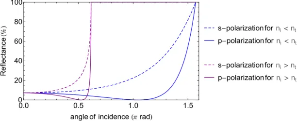
0.0 0.5 1.0 1.5 0 20 40 60 80 100
angle of incidence HΠ radL
Re fle ct a n ce H% L s-polarization for n i <nt p-polarization for ni <nt s-polarization for ni >nt p-polarization for ni >nt
Figure 2.4: Reflectance for s-polarization and p-polarization, when ni< nt and ni> nT.
The method for the calculation of the reflectance and transmittance for p-polarization is sim-ilar, the only difference is that instead of (0,E,0) we have (0, H,0).
Of particular interest is the angle at which p-polarization reflectance vanishes, see figure 2.4. This angle is called Brewster’s angle, at which the TM component is totally transmitted ¡Rp= 0¢. This angle is given by:
θB= cos−1 µ ni nt cosθt ¶ . (2.58)
When an EM wave propagates from a medium with lower refractive index, ni, to a medium
with higher refractive index, nt, Snell’s law is valid:
nisinθi= ntsinθt, (2.59)
because sinθt value is always less than 1, and therefore θtis real. However, if the medium of
incidence has a higher value, ni> nt, then it will exist one angle from which transmission will
not be possible for any polarization, due to the fact that sinθtwill be higher than 1 (according
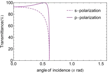
to Snell’s law), see figure 2.5.
The angle of incidence at which the transmitted angle reaches 90◦(or π/2 rad) is called the
critical angle θc, also known as the angle of total internal reflection. This angle can be
ex-pressed as:
θc= sin−1
ni
nt
. (2.60)
Consequently, if ni or ntis known, a careful measurement of the critical angle, θc, allows for
s-polarization p-polarization 0.0 0.5 1.0 1.5 0 20 40 60 80 100
angle of incidence HΠ radL
T ra n sm it ta n ce H% L
Figure 2.5: Transmittance of s-polarized and p-polarized electromagnetic waves for ni> nt.
Total internal reflection can be exploited in the use of attenuated internal reflection method (ATR) to guide light into thin films. This method is commonly used to inject or launch light into film optical waveguides.
2.5. SURFACE WAVES ANDATTENUATEDTOTALREFLECTION(ATR)
Beyond waves that propagate in free space, that can be for example plane or spherical, there are also the so-called surface waves. While the propagating waves are either longitudinal or transverse (while EM in free space can be only of the latter type), the surface waves are neither longitudinal nor transverse. They propagate along surfaces and interfaces and their amplitude decreases exponentially with the distance from the surface. Therefore they are also called evanescent waves. Elastic surface waves are known as Rayleigh waves and they propagate, for example, in the earth crust, faster then usual "bulk" sound waves.
As it will be discussed in the subsequent sections, surface EM waves can propagate at any in-terface between two dieletric media if their dielectric functions, ǫ1and ǫ2, obey the following
conditions:
ǫ1ǫ2< 0, (2.61)
and
ǫ1+ ǫ2< 0. (2.62)
The in-plane wavevector of such waves is large, q > ω/c ·max©p
ǫ1, pǫ2ª. For negative values
of the real part of the dielectric functions (ǫ1and ǫ2), q is imaginary and such modes lie to
the right side of the vacuum light line, in the ω-q plane. In other words, they cannot couple directly to propagating waves.
Coupling of propagating and evanescent waves becomes possible in so-called Attenuated Total Internal Reflection (ATR) configuration. The ATR experiment scheme is shown in figure 2.6. The light is reflected internally off the base of the prism at an angle of incidence which is higher than the critical angle to assure total internal reflection. This causes the in-plane wavevector component, q =pǫp ³ω c ´ sinθp, (2.63)
to be located adjacently to the base of the prism, where ǫp is the dielectric constant of the
prism. The excitation of surface polaritons happens when the field profiles of the surface polaritons and the evanescent wave overlap, i.e. when there is crossing of the ATR scanline and the dispersion curve of the surface mode. The energy from the light beam can couple
�� ��� � � � � � �� � � �� ��
Figure 2.6: ATR configuration. The yellow line corresponds to the surface polariton field while the brown one corresponds to the evanescent wave originated from the prism. only if the specimen is sufficiently close to the base of the prism. Therefore the prism is used to enhance the in-plane wavevector of the incident light, by placing it at the focus.
In terms of dispersion curves, the so-called ATR scanline is set to allow the coupling to occur:
c q = ωnpsinθp. (2.64)
The experimental outcome allows the study of the reflectivity of the beam.
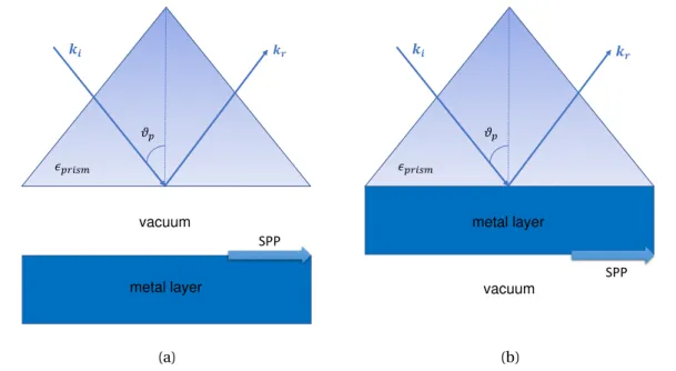
In the late sixties, Otto demonstrated the optical excitation of surface plasmons by the method of the ATR [9], see figure 2.7a. He showed that if a prism is placed near a metal-vacuum inter-face, SPPs can be excited optically by the evanescent wave originated from total reflection. In this configuration there is a finite gap between the prism and the metal layer and is suitable for surfaces which need to be changed easily. In the same year Kretschmann and Raether also proved that if a silver film is vaporized directly on the prism base surface (quartz), see figure 2.7b, there is also an excitation of a non-radiative mode on the boundary silver/air [10].
vacuum � � � � �� �� metal layer SPP (a) metal layer � � � � �� �� vacuum SPP (b)
3. S
URFACE PLASMON-
POLARITONS(SPP
S)
Surface plasmons are coherent oscillations of the free electron density near the surface, which exist at the interface between an insulator or vaccum and a conductor. This physical phe-nomenon will be studied in this chapter. Surface plasmon polaritons (SPPs) result from the coupling of surface plasmons with light. More specifically, the SPPs are evanescent waves with the following property, which will be discussed later:
q >pǫ1ω
c, (3.1)
where q ≡ kxis the SPP wavevector, which is paralell to the interface, and ǫ1is the dielectric
constant of the insulator.
3.1. SURFACE PLASMON-POLARITONS AT A METAL/DIELECTRIC SINGLE INTERFACE
3.1.1. DRUDE-SOMMERFIELD THEORY FOR METAL CONDUCTIVITY
Drude’s Model explains elementary properties of metals by regarding a metal as being essen-tially a free electron gas. The classical equation of motion for a free-electron gas, or basically a free electron localized in a metal which is subjected to an external field E = E0e−i ωtis:
d p(t )
d t = −
p(t )
τ − eE(t), for e > 0. (3.2)
Here, p(t) represents the electron momentum and τ is a phenomenological parameter known as relaxation time. If we calculate the Fourier transform of equation (3.2), one can easily obtain:
−i ωp(ω) = −p(ω)
τ − eE(ω). (3.3)
Hence, the frequency.dependent free electron momentum is:
p(ω) = e
iω − τ−1E(ω). (3.4)
Accounting the cumulative effect of all individual dipole moment of all free electrons, it is possible to express Jf(ω) as:
where e is the electric charge unit, ne is the electron density, and v(t) is the net velocity. Hence, Jf(ω) = enep(ω) me∗ = e2ne m∗e E(ω) Γ− i ω. (3.6) Here, m∗
e is the effective mass of the electron and Γ is damping parameter defined as:
Γ≡ τ−1. (3.7)
The damping parameter can also be interpreted as: Γ=vF
l , (3.8)
where l is the electron’s mean free path before scattering and vFrepresents the Fermi velocity.
Referring to subsection 2.2.1, we have now all the information necessary to obtain the Drude-type dielectric function:
ˆǫM(ω) = ǫ∞−
ω2p
ω2+ i Γω, (3.9)
where ωpis the plasma frequency and is defined as:
ω2p= 4πe
2n
e
me∗ . (3.10)
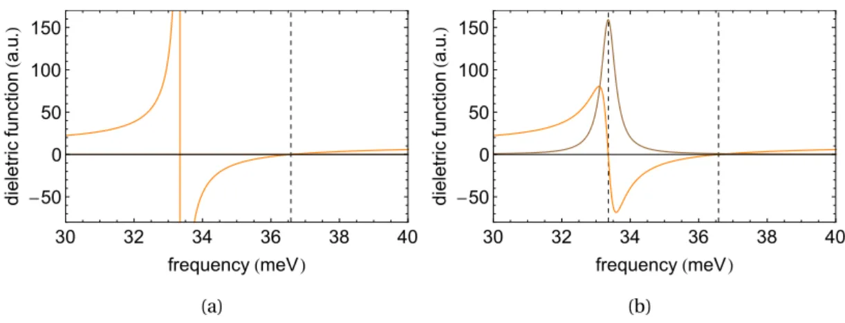
If we plot the Drude-type dielectric function for gold, presented in figure 3.4b, we clearly see that the real part is negative at low frequencies. Its physical interpretation is that the light can penetrate only to a very small extent, because the metal is conductive. On the other hand, in the same low frequency range the imaginary part of the complex function is strong, which describes the dissipation of energy associated with the motion of electrons in the metal. On a final note, the real part of the dielectric function approaches a fixed value for higher frequen-cies.
3.1.2. EXCITATION AND PROPAGATION OFSPPS
We shall consider two semi-infinite media separated by a plane interface as shown in figure 3.2. Both dielectric constants, ǫ1and ǫ2, are assumed real.
Real Imaginary 0 10 20 30 40 50 60 -1.0 -0.5 0.0 0.5 1.0 ΩHeVL d ie le c tr ic fu n c ti o n Ha .u .L
Figure 3.1: Plot of the real and imaginary parts of the Drude-type dielectric function for gold,
defined by the equation (3.34). The input parameters were ωp= 1.38 ∗ 1016s−1=
9.10eV and Γ = 1.08 ∗ 1014s−1= 0.07eV.
Using the mathematical identity (2.13), the homogeneous solutions (considering no external excitations) of the Maxwell’s equations at surface can be obtained from:
∇ × ∇ × E(r,ω) =ω 2 c2ǫ(r, ω)E(r, ω). (3.11) where ǫ(r, ω) = ǫ1(r,ω), if z > 0 ǫ2(r,ω), if z < 0
Let us consider a polariton constituted by two outgoing waves travelling away from the in-terface in the directions ±z. The electric field components for the TM polarization modes are: Ej= Ej x 0 Ej z
ei q x−i ωte±i kj zz, + for j = 1, and − for j = 2.
and
q2+ k2j z= ǫjk
2, j= 1,2. (3.12)
The wavevector k is defined as k =2πλ, where λ is the vacuum wavelength.
The displacement fields in both half spaces must be source free:
Consequently, we obtain the relation:
qEj x− kj zEj z= 0, j= 1,2. (3.14)
Therefore, we can express the evanescent wave equation as:
Ej= 1 0 ±kqj z
Ej xei q x−i ωte±i kj zz, + for j = 1, and − for j = 2.
Boundary conditions read:
E1x− E2x= 0 ǫ1E1z+ ǫ2E2z= 0
By applying equation (3.14) in these boundary conditions, and taking into account condition (2.61), we get the following relation:
ǫ1k2z+ ǫ2k1z= 0. (3.15)
Equation (3.15) has solution only if ǫ1ǫ2< 0. However, in this case at least on of the kj z, (y=1,2)
must be imaginary, so the other one also has to, otherwise (3.15) cannot be obeyed. Now we have all the information needed to obtain two important dispersion relations:
q2= ǫ1ǫ2 ǫ1+ ǫ2k 2, (3.16) and k2j z= ǫ2j ǫ1+ ǫ2k 2, j =1,2. (3.17)
To allow the propagation of waves along the interface, the vector q must be real. Conse-quently, the terms ǫ1ǫ2and ǫ1+ ǫ2, from equation (3.16), must be both positive or negative.
On the other hand, if we have a dielectric-metal interface, see figure 3.2, one must include losses associated with electron scattering (ohmic losses) which implies that the dielectric function must be complex. Consequently, the wavevector q will become complex:
�
�
�1
� �
Figure 3.2: Referential considered for the study of SPPs at an interface between air (ǫ1= 1)
and Gold, with a dielectric constant ǫ2(ω).
The q′ term is real and is used to determine the SPP wavelength. On the other hand, q′′
accounts for the damping of SPP’s as it propagates along the surface. Assuming that ||ǫ′′
1|| ≪
||ǫ′1||, the real and imaginary parts of the wavevector q are defined as:
q′≈ω c s ǫ′1ǫ2(ω) ǫ′1+ ǫ2(ω), (3.19) and q′′≈ω c s ǫ′1ǫ2(ω) ǫ′1+ ǫ2(ω) ǫ′′1ǫ2(ω) 2ǫ′ 1(ǫ′1+ ǫ2(ω)) , (3.20)
Additionally, the z components of the wavevector must be pure imaginary in both media to
obtain exponentially decaying results. Hence, the term ǫ1+ ǫ2, from equation (3.17), must be
negative. This gives us the conditions for the existence of localized modes: ǫ1· ǫ2(ω) < 0 ǫ1+ ǫ2(ω) < 0 ,
which was already mentioned above and also in section 2.5. Assuming that the dielectric medium has negligible losses, ǫ1will be real, i.e. ǫ1→ ǫ′1.
Furthermore, the parallel component of the wave vector k∥will have its real and complex
terms: Using equation (3.16) one can determine the SPP wavelength:
λSP P= 2π q′ ≈ λ s ǫ′1ǫ2(ω) ǫ′ 1+ ǫ2(ω) , (3.21)
One can substitute the wave vector modulus k in the evanescent field equation:
Ej= Ej x 0 Ej z
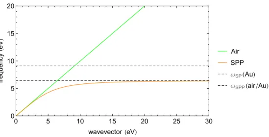
0 5 10 15 20 25 30 0 5 10 15 20 wavevector HeVL fr e q u e n c y He V L Air SPP ΩSPHAuL ΩSPPHair AuL
Figure 3.3: Dispersion relation of SPPs at an interface between air and gold (Au). The damp-ing factor was neglected. The solid orange line corresponds to the dispersion curve corresponds to bound SPPs modes, where its propagation is allowed. The green solid line corresponds to the dispersion function of a EM wave in air. The
dashed gray line corresponds to the plasma frequency of gold which is ωsp =
9.10eV. The dashed black line corresponds to the maximum frequency allowed
for the propagation of the SPPs which is ωspp= 6.43eV (equation (3.25)).
This makes it pretty clear that we are working with an evanescent wave which propagates in the ˆx direction, with a damping term e−q′′jx. Assuming that ||ǫ′′
1|| ≪ ||ǫ′1||, one can rewrite
equation (3.16) and easily obtain the dispersion relation of SPPs for a dielectric-metal inter-face: q =ω c s ǫ1ǫM(ω) ǫ1+ ǫM(ω) . (3.22)
By plotting the dispersion relation (3.22), we obtain the dispersion curve of single interface SPPs, shown in figure 3.3. The maximum frequency of the SPP dispersion curve plotted can be obtained if we set its slope to zero:
qc ω = s ǫ1+ ǫM(ω) ǫ1ǫM(ω) = 0 , (3.23) or just ǫ1+ ǫM(ω) = 0. (3.24)
Therefore the maximum frequency at which the SPP mode can be excited is:
ωSP P= 6.43 eV, (3.25)
which is also known as the electrostatic SPP frequency.
The propagation distance of the SPP along the interface is determined by q′′, which is
respon-sible for the exponential damping of the electric field amplitude. The damping is caused by ohmic losses of the electrons participating in the SPP and finally results in heating the metal.
3.2. SURFACE PLASMON-POLARITONS IN A DIELECTRIC/METAL/DIELECTRIC DOUBLE INTERFACE STRUCTURE
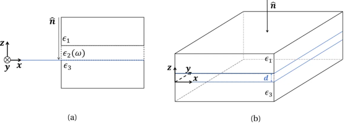
In this section it will be studied the transmission of light trough a gold film, of thickness d, surrounded by semi-infinite dielectric media, figure 3.4. It will only be considered TM
polar-� � � � ෝ� �3 �1 (a) � �1 ෝ� �3 � �3 � (b)
Figure 3.4: Choice of axes (a) and geometry (b) of a gold film (of thickness d) cladded by two
semi-infinite dielectrics. We consider ǫ1= 1 and ǫ3= 1, which correspond to air
media. The frequency-dependent dielectric function ǫ2(ω) corresponds to the
Drude dielectric function of gold. Therefore we consider a structure of a finite gold layer cladded by two semi-infinite air media.
ized fields: Hj(r, t) = ˆy ³ e−i kj zz+ ˆr pei kj zz ´ ei(q x−ωt) (3.26)
where ˆrpis the Fresnel reflection coefficient. Considering a non-magnetic material, we can
insert the magnetic field expression (3.26) into Maxwell’s equation: ∇ × Hj(r, t) =
ǫj
c
∂Ej(r, t)
to obtain the electric field amplitudes: Ej ,x= −i c ωǫj ∂zHj (3.28) Ej ,z= i c ωǫj ∂xHj, (3.29)
where j = 1,2,3. The values j = 1,3 correspond to the semi-infinite air media and j = 2 cor-responds to the gold medium:
1. In the dielectric medium j = 1, i.e. z > d, the fields are defined as:
H1(r, t) = ³ e−i k1z(z−d) + ˆrpei k1z(z−d) ´ ei(q x−ωt) , (3.30) and E1x(r, t) = − i c ωǫ1 ³ (−ik1z)e−i k1z(z−d)+ ˆrp(i k1z)ei k1z(z−d) ´ ei(q x−ωt) =c ω k1z ǫ1 ³ −e−i k1z(z−d)+ ˆr pei k1z(z−d) ´ ei(q x−ωt) . (3.31)
2. In the medium j = 2, at 0 ≤ z < d, we have assumed the unit magnetic field amplitude in the incident wave. Thus, we have:
H2(r, t) =
³ ˆ
ae−i k2zz+ ˆbei k2zz´ei(q x−ωt) , (3.32)
where ˆa and ˆb are unknown coefficients. The electric field is defined as: E2x(r, t) = − ic ω k2z ǫ2(ω) ³ ˆ a(−ik2z)e−i k2zz+ ˆb (i k2z)ei k2zz ´ ei(q x−ωt) =c ω k2z ǫ2(ω) ³ − ˆae−i k2zz + ˆbei k2zz´ei(q x−ωt) , (3.33)
where ǫ2(ω) is the real part of the Drude type dielectric function: ǫ2(ω) = 1 −
ω2p
ω2+ Γ2 , (3.34)
with ωpand Γ corresponding to the plasma frequency and damping factor, respectively,
and we put ǫ∞= 1 for simplicity.
3. Finally, the fields in the dielectric medium j = 3, i.e. z < 0, are:
H3(r, t) =ˆtpe−i k3zzei(q x−ωt) (3.35) E3(r, t) = − i c ωǫ3ˆtp(−ik3z)e −i k3zzei(q x−ωt) = − c ω k3z ǫ3 ˆtpe −i k3zzei(q x−ωt) . (3.36)
To determine the Fresnel coefficients ˆrpand ˆtp, we will use the transfer matrix method. The
continuity of fields at z = d can be expressed through the following boundary condition: H1(r, t) E1x(r, t) z=d+ = H2(r, t) E2x(r, t) z=d− . By writing it explicitly, we have
e−i k1z(z−d)+ ˆr pei k1z(z−d) c ω k1z ǫ1 ¡−e −i k1z(z−d)+ ˆr pei k1z(z−d) ¢ z=d+ ei(q x−ωt) = ˆ ae−i k2zz+ ˆbei k2zz c ω k2z ǫ2(ω)¡− ˆae −i k2zz+ ˆbei k2zz¢ z=d− ei(q x−ωt).
If we replace z for the respective value, we obtain: 1 + ˆrp c ω k1z ǫ1 ¡ ˆrp− 1 ¢ = ˆ ae−i k2zd+ ˆbei k2zd c ω k2z ǫ2(ω)¡− ˆae −i k2zd+ ˆbei k2zd¢ .
On the other hand, the fields at z = 0 are given by: H2(r, t) E2x(r, t) z=0+ = ˆ a + ˆb c ω k2z ǫ2(ω)¡− ˆa + ˆb¢ ei(q x−ωt), and H3(r, t) E3x(r, t) z=0− = ˆtp −ˆtpωc kǫ3z3 .
In order to determine the Fresnel coefficients ˆrpand ˆtpwe will use the transfer matrix method.
The most important aspect of using this method is that we are able to construct a matrix from which we can obtain ˆrpand ˆtpwithout the need to determine the coefficients ˆa and ˆb:
H2(r, t) E2x(r, t) z=0+ ≡ ˆT H2(r, t) E2x(r, t) z=d− . This implies that
H3(r, t) E3x(r, t) z=0− ≡ ˆT H1(r, t) E1x(r, t) z=d+ , i.e. ˆtp −ˆtpωc kǫ3z3 ≡ ˆT 1 + ˆrp c ω k1z ǫ1 ¡ ˆrp− 1 ¢ .
We can explicitly calculate the transfer matrix ˆT using the following equality: H2(r, t) E2x(r, t) z=0+ ≡ ˆT H2(r, t) E2x(r, t) z=d− , which gives us ˆ a + ˆb c ω k2z ǫ2(ω)¡− ˆa + ˆb¢ = ˆT ˆ ae−i k2zd+ ˆbei k2zd c ω k2z ǫ2(ω)¡− ˆae −i k2zd+ ˆbei k2zd¢ .
From here it is easy to obtain the matrix ˆT :
ˆ
a + ˆb = ˆT11¡aeˆ −i k2zd+ ˆbei k2zd¢ + ˆT12ωc ǫk2(ω)2z ¡− ˆae−i k2zd+ ˆbei k2zd¢
c ω k2z ǫ2(ω)¡− ˆa + ˆb¢ = ˆT21 ¡ ˆ ae−i k2zd+ ˆbei k2zd¢ + ˆT
22ωc ǫk2(ω)2z ¡− ˆae−i k2zd+ ˆbei k2zd¢ ,
(3.37) where ˆ T = ˆ T11 Tˆ11 ˆ T21 Tˆ21 . By solving the system of equations (3.37) we obtain
ˆ
T =
cos(k2zd) −iωc ǫ2k(ω)2z sin(k2zd )
−iωc k2z
ǫ2(ω)sin(k2zd ) cos(k2zd)
.
Now it is possible to determine the Fresnel coefficients working with the boundary condition: H3(r, t) E3x(r, t) z=0− ≡ ˆT H1(r, t) E1x(r, t) z=d+ , or H1(r, t) E1x(r, t) z=d+ ≡ ˆT−1 H3(r, t) E3x(r, t) z=0− , (3.38) where ˆ T−1= cos(k2zd) iωcǫ2k(ω)2z sin(k2zd ) iωc k2z ǫ2(ω)sin(k2zd ) cos(k2zd) . (3.39)
This translates to:
1 + ˆrp c ω k1z ǫ1 ¡ˆr p− 1¢ ≡ ˆT−1 ˆtp −ωc k3z ǫ3 ˆtp . (3.40)
By solving this we get: 1 + ˆrp= ˆT11−1ˆtp− ˆT22−1ωc kǫ3z3 , c ω k1z ǫ1 ¡ˆr p− 1¢ = ˆT21−1ˆtp− ˆT22−1ωc kǫ3z3 ˆtp. (3.41) After solving this system of equations we obtain:
ˆtp= ˆ 2 T−1 11−ωc k3z ǫ3Tˆ12−1−ωck1zǫ1 Tˆ21−1+k3zǫ3 k1zǫ1Tˆ22−1 , ˆrp= ˆtp³ ˆT11−1−ωc kǫ3z3 Tˆ12−1 ´ − 1 . (3.42) 3.2.1. DISPERSION RELATION
We know that ˆtp∝ Hi−1and we also know that in this case there is no incident wave.
Conse-quently, the dispersion relation can be obtained from the expression ˆt−1
p = 0: ˆ T11−1−c ω k3z ǫ3 ˆ T12−1−ω c ǫ1 k1z ˆ T21−1+k3z ǫ3 ǫ1 k1z ˆ T22−1= 0. (3.43)
In this section we assume that there is no damping and, consequently, ǫ2(ω) is real. Until now,
we have been working with purely imaginary wavevectors kz and ω real. It is convenient to
express the z components of the wavevectors in terms of a real quantity, x. However, we must pay attention to the signal since we want fields which don’t diverge when approaching the interface surface: −i k1z= κ1 where κ1> 0 , −i k2z= κ2 where κ2> 0 , −i k3z= κ3 where κ3> 0 . (3.44)
Substituting these real wavevectors in the dispersion equation (3.43), we obtain: ˆ Th,11−1 − ic ω κ3 ǫ3 ˆ Th,12−1 + iω c ǫ1 κ1 ˆ Th,21−1 +κ3 ǫ3 ǫ1 κ1 ˆ Th,22−1 = 0. (3.45) where ˆ Th−1=
i cosh(κ2d) −iωcǫ2κ(ω)2 sinh(κ2d )
−iωc κ2
ǫ2(ω)sinh(κ2d ) i cosh(κ2d)
.
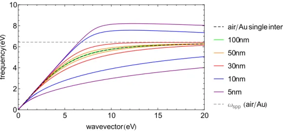
If we plot this dispersion equation we obtain the dispersion curve of the SPP, see figure 3.5. As the film thickness is decreased, the evanescent tails of the SPPs in each interface, z = d and z = 0, overlap, resulting in a split of two modes. The interaction between the EM fields
0 5 10 15 20 0 2 4 6 8 10 wavevectorHeVL fr e q u e n c y He V L
airAu single interface
5nm 10nm 30nm 50nm 100nm Ωspp HairAuL
Figure 3.5: Dispersion curves for different gold layer thickness values, considering an air/gold/air structure, Γ = 0. The black dashed line corresponds to the disper-sion curve for a single air/Au interface. The gray dashed line is the maximum
fre-quency allowed for the propagation of SPPs, which corresponds to ωspp= 6.43eV.
Solutions displayed above ωsppalso correspond to SPPs modes.
on different interfaces acts like a perturbation and breaks the degeneracy of the spectrum. To
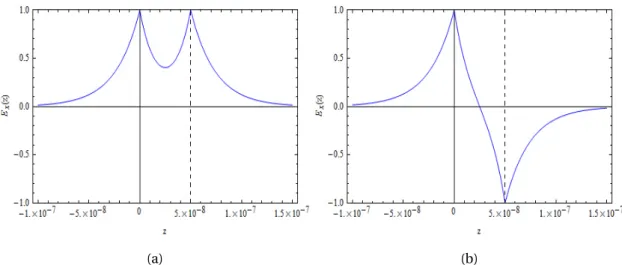
better understand these two different modes lets study the behavior of Ex(z).
In the absence of any incident wave, the field in the medium j = 1 is written as:
E1x(r, t) = c ω
k1z
ǫ1 ˆrpe
i k1z(z−d)ei(q x−ωt) . (3.46)
By substituting the real wavevectors in the electric field equations, we obtain: E1x(z) = iωc κǫ11ˆrpe−κ1(z−d), E2x(z) = iωc ǫ2κ(ω)2 ¡− ˆaeκ2z+ ˆbe−κ2z¢ , E3x(z) = iωc κǫ33ˆtpeκ3z. (3.47)
In order to calculate the coefficients ˆa and ˆb, we will work with the boundary condition:
ˆ a + ˆb c ω k2z ǫ2(ω)¡− ˆa + ˆb¢ = ˆtp c ω k3z ǫ3 ˆtp .
From this we obtain:
ˆ a =12ˆtp ³κ 2ǫ3+κ3ǫ2(ω) κ2ǫ3 ´ , ˆb =1 2ˆtp ³κ 2ǫ3−κ3ǫ2(ω) κ2ǫ3 ´ . (3.48)