© 2014 Rajalakshmi and Sudhakar, This open access article is distributed under a Creative Commons Attribution (CC-BY) 3.0 license
doi:10.3844/ajassp.2014.1343.1350 Published Online 11 (8) 2014 (http://www.thescipub.com/ajas.toc)
Corresponding Author: Rajalakshmi,T.R., Electronics and Communication Engineering, P.S.V College of Engineering and Technology, Krishnagiri, Tamilnadu, India
FAULT AND RELIABILITY ANALYSIS OF
CARBON NANO TUBE FET SRAM IN THE
PRESENCE OF SINGLE EVENT UPSET
1
Rajalakshmi,
T.R. and
2R. Sudhakar
1
Electronics and Communication Engineering,
P.S.V College of Engineering and Technology, Krishnagiri, Tamilnadu, India
2
Electronics and Communication Engineering,Dr. Mahalingam College of Engineering and Technology, Udumalai road, Pollachi, Tamilnadu, India
Received 2014-01-03; Revised 2014-03-07; Accepted 2014-05-28
ABSTRACT
Carbon nano tube devices are considered as a better replacement for CMOS technology nowadays due to its decreased sizing and increased performance. Resistive open and bridging faults play vital role in the dynamic fault analysis. These faults are important since the number of interconnects have increased. In this study we discuss the effect of open and bridging defects along with the variation of CNTFET parameters in the presence of Single Event Upsets (SEU). This helps us to analyse and have good comparison of CNTFET and CMOS SRAM faults in the presence of SEU. The analysis of these faults in the presence of SEU helps us to develop new efficient techniques to improve the performance. Presence of single event upset in the presence of these defects was analysed. The fault introduction in CNTFET SRAM showed different fault types for corresponding resistance values. The impact of resistive open defects and bridging defects on CNTFET SRAM in presence of SEU is estimated for different values of resistances compared close to CMOS SRAM.
Keywords: SRAM Carbon Nano Tube FET, Single Event Upset, Resistive Open Faults, Bridging Faults
1. INTRODUCTION
Due to advancements in nano electronics it is possible to build a trillion devices in a square cm. The reduced size and dense packing results in inaccuracies and instabilities during computation. These inaccuracies are due to fabrication process and also due to some external influences. These errors and influences are more prominent in NANO scale devices than in CMOS devices. In order to make these systems more reliable fault tolerance measurement and investigation of new faults become more important. This study analyses the impact of resistive open defects, bridging defects and the impact of alpha and neutron particles on these defects.
There are various types of resistive open defects that can be present in SRAM nodes. The objective of the paper is to
analyse CNTFET SRAM cells behaviour in the presence of resistive open defects under SEU radiation and to do the fault modelling in CNTFET SRAM.
2. PREVIOUS WORKS
nodes. The bridging defects have more impact on the core cells as the technology scales down. Its impact on nearby cells is also more. The work by Gil et al. (2009) explains how the manufacturing faults have greater impact in CNTFET logic circuits. It also deals with fault modelling of those mechanical defects. Cory et al. (2012) explained the sensitivity of CNTFET towards the radiation effects and have developed radiation hardening structures. Hamidreza and Lombardi (2007) deal with CNT defects and Defect analysis and single stuck at fault and bridging fault identification in CNTFET. Sivamangai and Gunavathi (2011) proposed a new technique to detect the faulty memory cells which reduces the number of March tests and reduces the time. Kotakoski et al. (2007) deals with basic effects of ion irrardiation on carbon nano tubes. The paper briefs out the change in the mechanical properties of the nano tube.
This study discusses the various types of defects which include resistive open and resistive bridging induced in CNTFET SRAM and the resulting fault models. It also discusses the impact on these defects when radiation ions hit the nodes. This study is structured as follows; the section II gives a brief introduction to various defects introduced and the possible fault occurrences. In section III experimental set-ups are described. In section IV impact of radiation is briefed, section V discusses the results and conclusion.
3. DEFECTS AND FAULTS
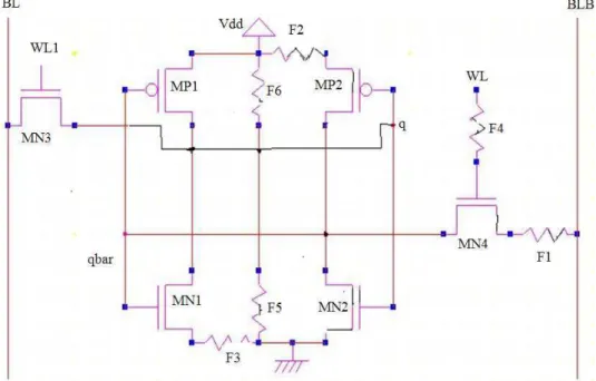
Resistive open defects in CNTFET SRAM are similar to that of the normal SRAM. These types of defects can be analysed by injecting defects in the circuit. The analysis is done for each defect separately. Multiple defects have lower impact on the small circuits hence separate defect impact alone is considered. The resistive open defects are placed in the CNTFET SRAM circuits as shown in the Fig. 1.
3.1. Faults Due to Resistive Open Defects
The defects can be summarised as follows:
F1- Deals with transition fault. It is noted during the write operation. This results in slow to rise and slow to fall of outputs. This is due to slow charging and discharging of node QBAR during writing process. It is easy to detect. F2- Data retention fault. This defect is placed on the pull-up transistor. This type of fault causes proper writing of values. The error occurs during the reading phase where the written value can be read for some period of time after which the value changes. F3- This defect induces delay during the discharge of the QBAR. This fault does not produce fault during the
first read. It needs subsequent process for further read. F4- This fault deals with stuck open where cells cannot be accessed for any operations. F5 and F6- Deals with stuck at faults.
The faults are first analysed for SRAM and then extended for CNTFET SRAM.
3.2. Resistive Bridging Defects
In this experimental set up resistive bridges have been made between nodes. Since the symmetry of the structure eases for analysis, not all the defect locations have been considered. Faults identified have been classified into two groups given by (Fonseca et al., 2010). Single cell faults and double cell faults. Resistances have been named as F1, F2, F3, F4 and F5. The types of fault have been identified due to these resistive bridges are stuck at fault, transition fault, no store fault, weak read fault, read destructive fault, incorrect read fault, disturb coupling fault. stuck at fault relates to cell being stuck in the same value irrespective of change in input. If a cell is unable to retain any logic information then the fault is identified as no store fault. During read operation the voltage difference between BL and BLB is less than 10% and then it is termed as Weak read fault and the last one deals with coupling fault. Each resistive bridge accounts to minimum of three faults.
3.3. Faults in CNTFET SRAM
Manufacturing defects like misaligned CNTs, open CNTS, poor contacts, doping errors cause various types of fault in CNTFETs. This includes Stuck at, improper logical behaviour and delay faults. Bridging of adjacent tubes can result in imperfect alignment and results in shorts. Studies of these faults and faults that have been evoked by environmental agents have been done in this study.
4. EXPERIMENTAL SETUP AND
METHODOLOGY
In this section experimental conditions for simulations to describe the fault analysis of CNTFET SRAM in the presence of Resistive defects, resistive bridging defects and SEU impact have been described. As shown in the Fig. 1 and 2 resistive set up was made. For ease of analysis core cell alone is considered and the analysis is made for single cell. The results were analysed with HSPICE tool. Stanford CNTFET model was used for coding.
Fig. 1. Resistive open defects
Fig. 2. Resistive bridging defects
4.1. Methodology
The analysis procedure starts with the development of 6T SRAM with CNTFET SRAM. The impact of single event upset is studied for CNTFET SRAM.
transistor based on the fault injection methods from Ammari et al. (2007). Here a double exponential model of current pulse is considered based on Riaz et al. (2007). The faults and Impact of SEU have been studied under this condition. The analysis is done for different diameters by changing the chiral values and for different technological nodes. For the ease of analysis single core cell was taken. Simulations have been with the variation in following parameters. We considered the defect value which ranges from few s to few G s:
• Technological node: 32, 22 and 10 nm • Diameter of CNTs: 1.024, 1.185 and 1.343 nm • Temperature: 25 and 125°C
5. IMPACT OF SEU IN THE
PRESENCE OF RESISTIVE DEFECTS
IN CNTFET SRAM
As stated by Rech et al. (2011) the impact of SEU in the presence of open defects in CNTFET SRAM had a greater impact in the SEU error rate.
As the m value varies from 13 to 19 the impact of SEU seemed to be less for the higher values of m. In case of resistive open defects the faults F3 and F5 are considered since they are connected to the N transistor where the effect of SEU has been studied.
The fault F3 which deals with read defect has been studied. The fault due to F3 showed little impact of SEU at higher value of resistance and flipping of cells was not observed. Resistance values varied from few M s to G s. The output was analysed for write operation and for hold state and the defect F5 which is stuck at fault was also
studied. Sequences of read operations were also applied to detect the fault in the presence of SEU. But flipping of cells was not observed for CNTFET SRAM cell.
Fault F4 induces error in writing operations while it does not affect read operation. In resistive bridging defects df2 and df3 are considered. Since the SEU is expected to affect the MN2 transistor.
Analyses were carried out for 22 and 32 nm CNTFET SRAM. As the size gets decreased the resistance values showed less impact on the fault df3. i.e., as the values varied from. 1 to 100 G, the fault was not observed in CNTFET SRAM.
6. RESULTS
First the measurement of voltage and current is done in the fault free circuit. The values of resistances causing the faults are measured. The fault is injected in the presence of single event upset. For SEU analysis current pulse was injected in mn2 transistor. The analysis is done for various temperature values and for various chiral and diameter variations. Table 1 and 2 discusses the variation in resistance value with respect chiral factor variation.
6.1. Resistive Open Defects
6.1.1. Resistive Bridging Defects
For both kind of analysis increase in temperature and diameter showed increase in faulty behaviour. During the leakage current analysis the leakage current in VDD node is more when compared to that of normal SRAM. Figure 3 deals with the effect of SEU in the presence of transition fault for CNTFET SRAM.
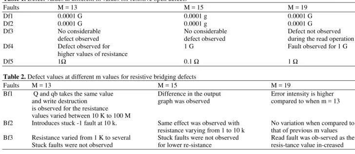
Table 1. Defect values at different m values for resistive open defects
Faults M = 13 M = 15 M = 19
Df1 0.0001 G 0.0001 g 0.0001 G
Df2 0.0001 G 0.0001 g 0.0001 G
Df3 No considerable No considerable Defect not observed
defect observed defect observed during the read operation
Df4 Defect observed for 1 G Fault observed for 1 G
higher values of resistance
Df5 1 0.1 1
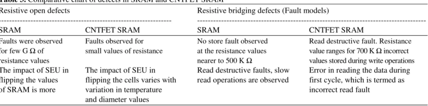
Table 2. Defect values at different m values for resistive bridging defects
Faults M = 13 M = 15 M = 19
Bf1 Q and qb takes the same value Difference in the output Error intensity is higher
and write destruction graph was observed compared to when m = 13
is observed for the resistance values varied between 10 K to 100 M
Bf2 Introduces stuck -1 fault at 10 k. Same effect was observed with No variation when compared to resistance varying from 1 to 10 k that of previous m values Bf3 Resistance varied from 1 K to several Stuck faults were not observed Read fault was ob-served as the
Table 3. Comparative chart of defects in SRAM and CNTFET SRAM
Resistive open defects Resistive bridging defects (Fault models)
--- ---
SRAM CNTFET SRAM SRAM CNTFET SRAM
Faults were observed Faults observed for No store fault observed Read destructive fault. Resistance for few G of small values of resistance at the resistance values value ranges for 700 K incorrect
resistance values nearer to 500 K values stored during write operations
The impact of SEU in The impact of SEU in Read destructive faults, slow Error in reading the data during flipping the values flipping the cells varies with read operations are observed first cycle, which is termed as
of SRAM is more variation in temperature incorrect read fault
and diameter values
Table 4. Comparison with previous works
SI.NO Previous works SRAM defect analysis CNTFET SRAM defect analysis
1 Fonseca et al. (2010) The faults were observed for few K s Faults were observed for MEG s to G incorrect read fault observed when march patterns were applied
2 Rech et al. (2011) Sensitivity to alpha particles is Faults are observed for very small values of increased with increase in resistance resistance. Variation in results observed values. Read stress operations are done for various Vt and diameter values
Table 3 lists out the comparison of occurrence of faults in SRAM and CNTFET SRAM. Table 4 compares the previous work with the obtained results.
7. DISCUSSION
The change chirality value affects the write behavior and consequently the fault natures. The change in the Diameter also brings out variation in the occurrence of defects.
In resistive open defects even for reduced values of defect resistance the CNTFET is susceptible to faults. Introduction of resistive open defects in CNTFET SRAM does not show much variation with that of CMOS SRAM. But different resistances introduce different types of fault when compared with CMOS SRAM.
When WL = 0 the cross coupled inverters are disconnected from bit lines and they showed no effect. The critical charge values varied as the values of F3 resistance is varied. As the resistance value is increased critical charge value also increased and is observed for both read and write operations.
When considering the defect rf2 the SEU is bringing mild change in the output, flipping is observed only for certain range of values and returns to original value after some period which is less when compared with that of rf1.
Impact of SEU have studied and analyzed by keeping the m value as 13 and n value as 0. When the circuit is subjected to single event transients, flipping was not observed in the case of bridging fault during write opera operation. The output voltage value rises with the rise in resistance values instead of inducing
the flipping. SEU impact was studied for the defect inducing resistance.
SEU occurrence was observed for WL = 0 and WL = 1. Occurrence of spike in every second write cycle has been observed for BF1 resistive bridging defect when the resistance value crosses 100 M.
Apart from normal read write problems CNTFET SRAM showed some new type of faults during read and write operations. These faults include the incorrect reading for a period of time and then coming back with original values. Most of the stuck faults which were observed for CMOS SRAM were not observed for CNTFET SRAM.
From Table 1 it had been inferred that the occurrence of fault comes with minimal resistance value as compared to SRAM.
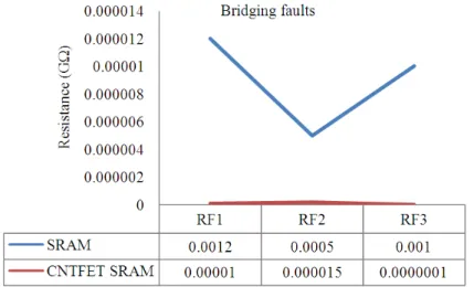
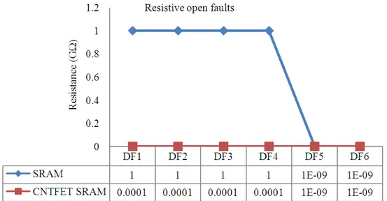
From Table 2 it had been inferred that the variation of the parameter M has impact on the change in the fault from Fig. 4 it is estimated that CNTFET SRAMS are easily susceptible to bridging faults when compared to SRAMs. This faults will result in the small amount of current flow which can be detected through the sensor circuits. Figure 5 gives resistance value comparison for resistive open faults.
The impact of SEU in CNTFET SRAM even for low energy radiation brings about changes in the output when compared to SRAM.
When comparing the previous works which projected the results of CMOS SRAM, this study elaborates the defects and single event upsets in CNTFET SRAM.
On comparing the fault effects and SEU, the CNTFET SRAM shows slightly different behavior compared to CMOS SRAM. The type of faults observed also varies with CNTFET SRAM.
Fig. 5. Comparative chart of variation in resistance parameter for each fault with respect to SRAM and CNTFET SRAM
8. CONCLUSION
In this study the effect of environmental agents in the presence of resistive defects is experimented. March algorithms and variant of March algorithms were used for the study of faults. In this study sensitivity of CNTFET SRAM for resistive open and bridging defects in the presence of alpha particles have been studied. Also the comparative study on effects of resistive open and resistive bridging defects in CMOS SRAM and CNTFET SRAM has been made. The impact of Single Event upset on these faults has also been studied. It is identified that during bridging faults the effect of flipping is affected .During resistive open defects, fault variations are observed in CNTFET SRAM when compared to normal CMOS SRAM. Some of the faults were detected using March algorithm; while for others efficient algorithms are needed to detect the faults. This study delineates the comparative study of CNTFET SRAM and CMOS SRAM in the presence of resistive defects. Transient current analysis is also made. This study will be helpful for further enhancements in fault analysis, fault detection and correction circuitries and in the development of Built in current Sensors for CNTFET SRAM. Since CNTFET SRAMS require more accurate sensors and error detectors compared to CMOS SRAM, the studies done through this study will be helpful in developing such systems.
9. REFERENCES
Ammari, A., L. Anghel, R. Leveugle, C. Lazzari and R. Reis, 2007. SET fault injection methods in analog circuits: Case study. TIMA Laboratory.
Cory, C.D., J.J. McMorrow, J.T. Robinson, B.J. Landi and S.M. Hubbard et al., 2012. Radiation effects in carbon nanoelectronics. Electronics, 1: 23-31. DOI: 10.3390/electronics1010023
Fonseca, R.A., L. Dilillo, A. Bosio, P. Girard and S. Pravossoudovitch et al., 2010. Analysis of resistive-bridging defects in SRAM core-cells: A comparative study from 90nm down to 40nm technology nodes. 15th IEEE European Test Symposium, May 24-28, IEEE Xplore Press, Praha, pp: 132-137. DOI: 10.1109/ETSYM.2010.5512768
Gil, D., D. de Andrés, J.C. Ruiz and P. Gil, 2009. Impact of manufacturing defects on carbon nanotube logic circuits. Proceedings of the 3rd
Workshop on Dependable and Secure
Nanocomputing, Jun. 29-29, Fault-Tolerant Systems Group,Portugal, pp: 1-14.
Kotakoski, J., A.V. Krasheninnikov and K. Nordlund, 2007. Atomistic simulations of irradiation effects in carbon nanotubes. Radiat. Effects Defects
Solids, 162: 157-169. DOI:
10.1080/10420150601132537
Riaz, N., Y. Boulghassoul, J. Draper, D. Sandeepan and A. Witulski, 2007. Critical charge characterization for soft error rate modeling in 90nm SRAM. Proceedings of the IEEE International Symposium on Circuits and Systems, May 27-30, IEEE Xplore Press, New Orleans, LA, pp: 1879-1882. DOI: 10.1109/ISCAS.2007.378282
Rech, P., J.M. Galliere, P. Girard, F. Wrobel and F. Saigne et al., 2011. Impact of resistive-open defects on SRAM error rate induced by alpha particles and neutrons. IEEE Trans. Nuclear Sci., 58: 855-861. DOI: 10.1109/TNS.2011.2123114 Sivamangai, N.M. and Gunavathi, 2011. Design for
test technique for leakage power reduction in nanoscale static random access memory. J.
Comput. Sci., 7: 1252-1260.