Universidade de Aveiro 2015
Departamento de Eletrónica, Telecomunicações e Informática
Hélder Alexandre
Machado Cardoso
Amplificadores de Baixo Ruído para Aplicações em
Radioastronomia
Universidade de Aveiro 2015
Departamento de Eletrónica, Telecomunicações e Informática
Hélder Alexandre
Machado Cardoso
Amplificadores de Baixo Ruído para Aplicações em
Radioastronomia
Dissertação apresentada à Universidade de Aveiro para cumprimento dos requisitos necessários à obtenção do grau de Mestre em Engenharia Eletrónica e Telecomunicações, realizada sob a orientação científica do Professor Doutor Luis Filipe Mesquita Nero Moreira Alves, Professor Auxiliar do Departamento de Eletrónica, Telecomunicações e Informática da Universidade de Aveiro.
O Júri
Presidente Prof. Dr. José Carlos Esteves Duarte Pedro
Professor Catedrático do Departamento de Eletrónica, Telecomunicações e Informática da Universidade de Aveiro
Arguente Dr. Luis Manuel Santos Rocha Cupido
Diretor Executivo da LC Technologies
Prof. Dr. Luis Filipe Mesquita Nero Moreira Alves
Professor Auxiliar do Departamento de Eletrónica, Telecomunicações e Informática da Universidade de Aveiro
Agradecimentos Agradeço aos meus pais, avó, irmã e irmão pela educação, pelas condições que me proporcionaram durante estes anos de formação e pelo apoio e confiança demonstrados em todas as etapas da minha vida. Ao Frederik e à Rosário pelo apoio, confiança e ajuda em tornarem o impossível em realidade. À Mateja pela sua presença, confiança e apoio incondicional. Aos meus amigos mais próximos pela sua amizade e por todos os momentos partilhados.
Agradeço ao meu orientador, o Professor Doutor Luis Nero, pela oportunidade proporcionada, pelo apoio e preocupação demonstrados ao longo do trabalho. Agradeço, em especial, ao Mestre Miguel Bergano pelo auxílio essencial em todas as etapas do desenvolvimento deste trabalho, pelas críticas construtivas efetuadas ao longo do mesmo, pela motivação transmitida e pelo companheirismo. Agradeço ao Paulo Gonçalves do corpo técnico do Instituto de Telecomunicações pela disponibilidade e auxílio na implementação dos circuitos. Agradeço também ao Instituto de Telecomunicações pelas condições proporcionadas durante a realização deste trabalho.
Palavras-chave Amplificador de Baixo Ruído, Ruído Térmico, Temperatura de Ruído, Figura de Ruído, Radioastronomia, Banda X, Simulação, Desenho, Eletrónica de
RF/Microondas
Resumo Atualmente, a investigação do Universo representa um desafio enorme para a Humanidade e qualquer descoberta ou inovação é sempre significativa. A radioastronomia tem sido responsável por alguns destes avanços tais como a descoberta de pulsares e da radiação cósmica de fundo em microondas. O nosso conhecimento acerca do Universo é ainda limitado e esta busca pelo desconhecido continua. A prova disso mesmo está no início da construção do Square Kilometre Array que é rotulado como o maior e mais sensível radiotelescópio do mundo. Este projeto vai abrir novos horizontes na descoberta científica e terá como objectivo responder a algumas questões fundamentais da astronomia.
Este trabalho enquadra-se precisamente na área da radioastronomia. Inovação nesta área de investigação exige o desenvolvimento e o teste de novas tecnologias de recetores de radioastronomia. A necessidade de elevada resolução exige recetores contribuindo com pouco ruído relativamente à medição a efetuar e uma largura de banda muito maior do que um sistema de telecomunicações normal. O componente crítico no desempenho do recetor em termos de ruído é o amplificador de baixo ruído.
Este trabalho de Mestrado consiste no desenho e implementação de um amplificador de baixo ruído funcional na banda X para ser selecionado como candidato para uma experiência em radioastronomia. Os resultados da simulação do amplificador e do respetivo desempenho em laboratório também estão documentados.
Keywords Low-Noise Amplifier, Thermal Noise, Noise Temperature, Noise Figure, Radio Astronomy, X Band, Simulation, Design, RF/Microwave Electronics.
Abstract Nowadays, understanding the Universe still represents a great challenge for the mankind and what may look like a small step forward becomes a huge leap all from a sudden. Radio astronomy has been responsible for some of these huge scientific leaps with many discoveries made in radio frequencies such as the discovery of pulsars and the cosmic microwave background. Our knowledge about the Universe is still limited and this search for the unknown continues. Evidence of this is the beginning of the construction of the Square Kilometre Array that is labeled as the world's largest and most sensitive radio telescope. This project will lead the way in scientific discovery and will aim to solve some of the biggest questions in the field of astronomy.
This work precisely falls within the radio astronomy scientific field. Advances in radio astronomy research require the development and evaluation of new technologies of radio astronomy receivers. The demanding of higher resolution requires receivers with front-ends adding low noise relatively to the weak signal to measure and a wider bandwidth than an average telecommunication system. The critical component of a receiver in terms of noise performance is the low-noise amplifier.
This Master's thesis consists in the design and implementation of a low-noise amplifier operating within the X band to be selected as a candidate for a radio astronomy experience. The simulation results of the amplifier and the respective performance in a laboratory environment are also presented.
Contents
Contents ... I List of Figures ... V List of Tables ... IX List of Acronyms ... XI 1 Introduction ... 1 1.1 Motivation ... 2 1.2 Purpose ... 41.3 Structure of the Document ... 5
2 Fundamental Concepts ... 7
2.1 Noise Characteristics ... 7
2.1.1 Noise Voltage ... 8
2.1.2 Noise Power ... 9
2.1.3 Noise Temperature ... 11
2.1.4 Signal-to-Noise Power Ratio ... 15
2.1.5 Noise Factor ... 17
2.1.6 Noise Figure ... 18
2.1.7 Multistage Systems ... 19
2.2 Noise Measurement ... 22
2.2.1 Noise Power Linearity ... 23
2.2.2 Noise Source ... 24
2.2.3 Y-Factor Method ... 25
2.3.1 Scattering Parameters ... 27
2.3.2 Power Transport and Gain ... 29
2.3.3 Noise Parameters ... 33
2.4 Low-Noise Amplifier Design ... 34
2.4.1 Stability Considerations ... 35
2.4.2 Gain Match ... 38
2.4.3 Noise Match ... 41
3 Design and Simulation ... 43
3.1 Two-Stage Low-Noise Amplifier Design Method... 43
3.2 Components Selection ... 44
3.2.1 Printed-Circuit-Board ... 44
3.2.2 Active Device Selection ... 45
3.2.3 Passive Devices ... 46
3.3 DC Block Design ... 47
3.3.1 Capacitor ... 47
3.3.2 Parallel Coupled-Line Filter ... 50
3.4 Transistor Analysis ... 51
3.4.1 Model Validation ... 51
3.4.2 DC Bias Networks ... 53
3.4.3 Stability Check and Enhancement ... 55
3.4.4 DC Simulation ... 58
3.5 Matching Networks Design ... 58
3.6 Simulation Results ... 60
3.7 Layout and Implementation ... 62
4 Measurement and Results ... 67
4.1 Network Measurements... 67
4.1.2 Results ... 69
4.2 Noise Measurements ... 71
4.2.1 Equipment and Setup ... 71
4.2.2 Measurement Corrections ... 72
4.2.3 Unavoidable uncertainties ... 74
4.2.4 Results ... 76
5 Conclusion and Future Work ... 83
5.1 Conclusion ... 83
5.2 Future Work ... 85
Appendices ... 87
A. The Radiometer ... 87
A.1 Black-body Radiation ... 87
A.2 Brightness Source Temperature ... 88
A.3 Antenna Noise Temperature ... 89
A.4 The Total Power Radiometer ... 90
B. Additional Low-Noise Amplifiers Designed ... 92
List of Figures
Figure 1: Sources of external noise [60]. ... 1
Figure 2: A typical radio telescope [53]. ... 3
Figure 3: Power spectrum of noise in a device [61]. ... 8
Figure 4: Random voltage generated by a resistor [60]. ... 9
Figure 5: Equivalent circuit of a noise transfer situation. ... 10
Figure 6: Noise power measurement of an excited noisy network [34]. ... 11
Figure 7: Modelling of a noisy device with an output noise source. ... 12
Figure 8: Modelling of a noisy device with an input noise source. ... 13
Figure 9: Effective input noise temperature concept [34]. ... 14
Figure 10: Power considerations of a noisy network [60]. ... 16
Figure 11: How noise builds up in a multistage system [31, 34]. ... 19
Figure 12: Noise figure measurement setup. ... 23
Figure 13: Linear two-port network noise power characteristic [31]... 23
Figure 14: Schematic of an active noise source [3]. ... 24
Figure 15: Representation of the Y-factor Method [31, 60]. ... 25
Figure 16: General two-port network [40]. ... 27
Figure 17: Practical case of a general two-port network. ... 28
Figure 18: General two-port network with arbitrary source and load impedances. 30 Figure 19: Noisy two-port network described by its noise parameters. ... 33
Figure 20: The general transistor amplifier circuit [40]. ... 35
Figure 21: Stable and unstable regions in the Γ𝐿 plane [23]. ... 37
Figure 22: Stable and unstable regions in the Γ𝑆 plane [23]... 37
Figure 24: Substrate Parameters. ... 45
Figure 25: Equivalent circuit of a microwave capacitor. ... 48
Figure 26: Insertion loss of the selected capacitor. ... 49
Figure 27: Return loss of the selected capacitor. ... 49
Figure 28: Magnitude of impedance of the selected capacitor. ... 50
Figure 29: Parallel coupled-line filter. ... 50
Figure 30: Insertion loss of the parallel coupled-line filter. ... 51
Figure 31: Scattering parameters validation for the MGF4937AM. ... 52
Figure 32: Noise data validation for the MGF4937AM. ... 53
Figure 33: Biasing scheme. ... 54
Figure 34: DC bias network performance. ... 55
Figure 35: Stabilization network. ... 56
Figure 36: Stabilization network response. ... 56
Figure 37: DUT for design (MGF4937AM). ... 57
Figure 38: Characteristics of the DUT for design (MGF4937AM). ... 57
Figure 39: Noise figure and gain simulations. ... 61
Figure 40: Return loss and overall stability simulations. ... 61
Figure 41: Layout of the implemented amplifier. ... 63
Figure 42: Assembly information for the implemented amplifier. ... 64
Figure 43: Complete assembled board with dimensions 20 x 64 mm. ... 65
Figure 44: Scattering parameters measurement setup... 68
Figure 45: Input return loss (left) and isolation (right). ... 69
Figure 46: Output return loss (left) and gain (right). ... 70
Figure 47: Stability analysis: K factor (left) and ∆ (right). ... 70
Figure 48: Component placement in the measurement of noise figure. ... 72
Figure 49: Uncertainty model. ... 75
Figure 50: Uncorrected and corrected DUT noise performance. ... 76
Figure 52: Uncorrected and corrected instrument noise figure. ... 77
Figure 53: Comparison of simulated and measured DUT noise performance. ... 77
Figure 54: Comparison of simulated and measured DUT gain with measurement validation by two instruments. ... 78
Figure 55: Measurement uncertainty as function of the frequency. ... 78
Figure 56: Measurement uncertainty as function of the DUT noise figure. ... 79
Figure 57: Measurement uncertainty as function of the DUT gain. ... 79
Figure 58: Measurement uncertainty as function of the instrument noise figure. .. 80
Figure 59: Measurement uncertainty as function of the DUT input match (reflection coefficient). ... 80
Figure 60: Measurement uncertainty as function of the DUT output match (reflection coefficient). ... 81
Figure 61: Noise figure uncertainty in the DUT. ... 81
Figure 62: Source brightness temperature of an arbitrary white noise source [60]. 89 Figure 63: Total power radiometer block diagram [60]. ... 90
Figure 64: LNA designed with the cascade of single stages method (MGF4937AM). ... 93
Figure 65: LNA designed with the single interstage matching network method (MGF4937AM). ... 94
Figure 66: LNA designed with the cascade of single stages method (MGF4937AM and MGF4941AL). ... 95
Figure 67: LNA designed with the single interstage matching network method (MGF4937AM and MGF4941AL). ... 96
List of Tables
Table 1: LNA required performance. ... 4 Table 2: Biasing values during simulation. ... 58 Table 3: LNA simulated performance. ... 62 Table 4: Bill of materials of the implemented amplifier. ... 65 Table 5: Biasing values during measurement. ... 68 Table 6: Noise figure measurement including associated uncertainty. ... 82 Table 7: LNA measurement results. ... 84
List of Acronyms
ADS Advanced Design System DC Direct Current
DUT Device Under Test EM Electromagnetic
EMI Electromagnetic Interference EMR Electromagnetic Radiation ENR Excess Noise Ratio
ESL Equivalent Series Inductance (L is inductance) ESR Equivalent Series Resistance
GPS Global Positioning System IF Intermediate Frequency
IIP3 Third Order Input Intercept Point LNA Low-Noise Amplifier
MAG Maximum Available Gain MIM Metal-Insulator-Metal MSG Maximum Stable Gain PCB Printed-Circuit-Board
PRF Parallel Resonant Frequency PSD Power Spectral Density RF Radio Frequency
RL Return Loss
RMS Root Mean Square SKA Square Kilometre Array SMA SubMiniature version A SMD Surface Mount Device
SNR Signal-To-Noise (Power) Ratio SOLT Short-Open-Load-Through SRF Series Resonant Frequency
Chapter I
1
Introduction
The performance of communication systems is limited by noise, which can be coupled into a receiver or generated within the system itself. In either case, the noise level of the system establishes the threshold for the minimum signal detected by a receiver in the presence of noise. Noise is a random signal and generally may be defined as any unwanted form of energy yet unavoidable which tends to interfere with the proper reception and reproduction of a desired signal. However, the desired signal in some cases, such as radiometers or radio astronomy systems, is actually noise power collected by an antenna [60].
Noise, regarding its source, can be put into two categories: external noise and internal noise. External noise, i.e. noise whose sources are external, may be inserted into a system either by a receiving antenna or via electromagnetic interference (EMI).
External noise has neither a specific frequency nor direction, and consequently, some external noise will always be present in a system regardless the receiver’s tuning frequency or the antenna’s pointing direction. External noise can be classified as terrestrial or extra-terrestrial. The former, as its name suggests, is connected to warm objects and phenomena on the Earth (Figure 1). It can be due to natural causes (atmospheric and ground noise) or generated by humans (man-made/industrial noise). There are also very warm objects in outer space – sources of extra-terrestrial noise. Hereupon, due to the proximity of those sources to Earth, extra-terrestrial noise can be put into two subgroups: the noise produced by distant celestial bodies, such as stars and planets, can be classified as cosmic noise while the noise emanating from the Sun can be classified simply as solar noise.
Internal noise, however, consists in noise generated within a receiver, communication system or electrical device including resistors and semiconductors. All those objects are noisy by some degree, and therefore a general receiver not only amplifies the desired signal along with the external noise coupled into the system but also adds noise that it internally generates. Thus, it is generally desired to minimize the residual noise level of a system to achieve the best performance. The first stage of a receiver front-end has the dominant effect on the noise performance of the system, and therefore a preamplifier contributing with low noise to the system but presenting enough gain to boost the power of the input signal above the receiver noise floor is required. The device providing such a performance is a low-noise amplifier (LNA) and plays an important role as a building block of any communication system. The LNA is an amplifier used to capture and amplify very weak signals and the random noise presented at its input within the bandwidth of interest. Low-noise amplifiers are used in many applications that involve the detection of very weak signals. Several wireless communication applications demand low-noise amplifiers with distinct specifications and some examples are in mobile phones, global positioning system (GPS) receivers, satellite communication systems or radio astronomy receivers.
1.1
Motivation
This work falls within the radio astronomy scientific field. Radio astronomy is the study of celestial bodies at radio wavelengths and seeks to detect and measure the extremely weak electromagnetic radiation (EM radiation or EMR) from distant
celestial sources [8, 52]. Microwave radiometry, which plays a significant role in remote sensing, is of interest in radio astronomy. Radiometry, in general, is a passive method of detecting the radiation of matter. Its techniques extract information about a target from the intensity and spectral distribution of its emitted electromagnetic radiation, either detected directly or through reflection from surrounding bodies, allowing the thermal characterization of the radiant body as well as its environment, all independently of distance [60]. This EMR power, i.e. noise, is measured by a specially designed sensitive receiver called radiometer [60, 65].
The observations conducted in microwave radiometry employ antenna receiver systems called radio telescopes in radio astronomy. A radio telescope can be described, in its simplest form, by a directional antenna, pointing towards the sky, connected to a low-noise receiver [19].
Figure 2: A typical radio telescope [53].
Nowadays, radio telescopes commonly employ dish-shaped antennas (Figure 2) that can be pointed toward any part of the sky in order to gather up the radiation and reflect it to a central focus where the weak electric current, induced by the radio waves, can then be amplified by a receiver making use of the lowest noise preamplifiers that can be produced these days, in order to boost a weak signal to a measurable level [19]. The low-noise receiver is merely a microwave radiometer whose goal, in practice, is to measure the power radiated by astronomical objects [54]. This signal power level is commonly quite low, and so a radiometer for passive microwave radiometry demands high sensitivity to be able to detect extremely small signal powers.
New advances in radio astronomy demand high-performance receivers, and therefore low-noise amplifiers with better performance are essential. Current technology development and radio astronomy research have already enabled the planning and the beginning of the construction of the next-generation radio telescope that will far exceed the capabilities of any existing radio telescope: the Square Kilometre Array (SKA) [68]. The SKA is an international radio astronomy effort to build the world’s largest and most sensitive radio telescope consisting of thousands of antennas linked together by high bandwidth optical fiber, and so has attracted the attention of the radio astronomers around the globe [7, 67]. The SKA is a long term project with a phased approach built over two sites: an infrastructure will take place in Western Australia and another will be deployed in southern Africa [67, 68, 69]. The SKA project implies deploying thousands of radio telescopes in three unique configurations in a manner that they will work together as one gigantic virtual instrument allowing international scientists to make ground-breaking observations and discoveries about the Universe [67, 68]. Thus, the SKA will perfectly augment, complement and lead the way in scientific discovery [58].
1.2
Purpose
A low-noise amplifier was required for an X-band receiver application. The device proposed required the following performance:
Table 1: LNA required performance.
Parameter Performance Unit
Center Frequency 10 GHz Bandwidth ≥ 500 MHz Gain ≥ 15 dB Noise Figure ≤ 0.4 dB Input Impedance 50 Ω Output Impedance 50 Ω
No requirements were imposed in terms of linearity, such as the third order input intercept point (IIP3), or in terms of supply voltage or current. Additionally, in terms of input and output impedances, there will always be a mismatch to the required 50 Ω that can be measured in terms of return loss (RL), and therefore the values to obtain should be the best possible. In order to fulfil the design goals, a two-stage transistor amplifier approach was chosen.
1.3
Structure of the Document
Besides this opening chapter, this document contains four additionally chapters. Chapter II outlines the fundamental concepts concerned with a LNA. It starts by characterizing and quantifying noise at device level and extending the concepts to a system level where the basics of noise measurement are briefly presented. Furthermore, two-port networks are described in terms of representation and characteristic parameters in order to introduce the design considerations and techniques common to LNA design.
Chapter III covers the design steps of the LNA, the expected results obtained via simulation and the implementation of the device.
Chapter IV deals with the measurements carried out in a laboratory environment by taking in account cautions and corrections in order to improve accuracy. The procedure adopted is explained in detail and the results are presented. Chapter V ends this document with an overview of the work and an analysis of the results, evaluating limitations and considering further improvements to apply while designing a LNA as well as additional ideas to accomplish in future works.
Chapter II
2
Fundamental Concepts
The internally generated noise is a key performance parameter in a LNA, and therefore this chapter starts with a brief description of noise characteristics, how it can be quantified in a device and the extension of the concept to a system. Thereafter, the fundamental features of noise measurement are discussed. The chapter also covers the behavior of two-port networks and how their performance can be characterized. Finally, the last section focuses on the analysis and techniques employed for the design of a LNA.
2.1
Noise Characteristics
The noise internally generated in a device or component is usually caused by the random motion of charge carriers, which in turn constitutes a fluctuating alternating current that can be detected as random noise [34]. Such motions may be due to several mechanisms, leading to various types of noise in electrical circuits.
Thermal noise, also known as Johnson or Nyquist noise, occurs due to vibrations of conduction electrons and holes due to their finite temperature [31]. Shot noise arises from the quantized and random nature of current flow and normally occurs when there is a potential barrier [31]. The power spectrum of both thermal and shot noises is essentially uniform across the entire radio and microwave ranges. Thus, thermal and shot noises are examples of white noise over those regions. Flicker noise, also known as pink noise, is basically any noise whose power spectrum varies inversely with frequency, and so is often called 1/f noise [60]. Thus, it is dominant only at low frequencies.
Noise characterization usually refers to the combined effect from all the causes in a component [61], as shown in the following figure.
Figure 3: Power spectrum of noise in a device [61].
At microwave frequencies, the combined effect is often referred to as if it all were caused by thermal noise [31].
2.1.1 Noise Voltage
The random motion of charge carriers is caused by heating, which in turn is connected to resistive loads when dissipating energy. Thus, thermal noise is always linked with resistance values, and therefore a resistor can serve as a noise generator. All random motion stops at absolute zero [34], i.e. 0 Kelvin, and so any object whose temperature is above the absolute zero is said to be warm, and therefore generates noise [55]. Thus, a resistor at a physical temperature above 0 Kelvin generates noise. The free electrons in this resistor are in random motion with a kinetic energy proportional to the temperature, which in turn creates a small electric field within the device, and therefore produces a small, random voltage, 𝑢𝑛(𝑡), across the resistor [60], as it can be seen in the following figure.
Figure 4: Random voltage generated by a resistor [60].
The instantaneous value of noise cannot be predicted since noise is a random signal, and therefore it cannot be characterized deterministically. However, it can be described statistically, i.e. in terms of average values [61]. Although the random voltage has a zero average value, 〈𝑢𝑛(𝑡)〉, it can still be characterized statistically by
either noise variance, 〈𝑢𝑛2(𝑡)〉, or root mean square (RMS) value, √〈𝑢 𝑛 2(𝑡)〉.
The RMS value of the random noise voltage is given, in Volt, by
𝑈𝑛 = √ 4ℎ𝑓𝑅𝐵
𝑒ℎ𝑓 𝑘𝑇⁄ − 1 (1)
where 𝑇 is the physical temperature of the resistor in Kelvin, 𝑅 is the resistance in Ohm, 𝑓 stands for the center frequency, in Hertz, of the finite system bandwidth 𝐵, also in Hertz while 𝑘 = 1.380 × 10⁻²³ 𝐽/𝐾 and ℎ = 6.626 × 10⁻³⁴𝐽𝑠 are the Boltzmann and Planck constants, respectively.
However, the above result can be reduced to Johnson’s formula [30] for open circuit noise voltage when the Rayleigh-Jeans limit applies, i.e. whenever the condition ℎ𝑓 ≪ 𝑘𝑇 is satisfied [51, 60].
𝑈𝑛 = √4𝑘𝑇𝑅𝐵 (2)
This last result is commonly used in microwave circuit design.
2.1.2 Noise Power
The noise generated by a thermal noise source, such as a resistor, can be transferred to the remaining circuit. A general result can be obtained by connecting
a source impedance, at a temperature above absolute zero, to a load impedance where both of them have real part, i.e. a resistance value. Every microwave circuit has a finite bandwidth that will limit the amount of noise power that is transferred. Due to this fact, let us consider an ideal bandpass filter perfectly matched connected between the source and the load impedances as shown in the figure below.
Figure 5: Equivalent circuit of a noise transfer situation.
Each resistance generates random currents, and in thermal equilibrium the power generated by each one of them is equal to the power absorbed, i.e. the noise power transferred in one direction is equal to the one transferred in opposite direction [57]. The average noise power, in Watt, transferred to the load is equal to
𝑃𝑛 =
𝑈𝑛2
(𝑅𝑒{𝑍𝑆+ 𝑍𝐿})2+ (𝐼𝑚{𝑍𝑆+ 𝑍𝐿})2𝑅𝑒{𝑍𝐿}
(3)
where 𝑈𝑛 is the noise voltage, as given by Equation 2, produced by the source resistance. This quantity reaches a maximum when impedance matching is verified, i.e. 𝑍𝑆 = 𝑍𝐿∗, and therefore maximum noise power transfer is obtained. So, the thermal noise power delivered by a resistor into an impedance matched load is
𝑃𝑛 = 𝑘𝑇𝐵 (4)
This result gives the maximum available noise power from a noisy resistor at a physical temperature 𝑇, and due to this fact is also called the available noise power. At any temperature above absolute zero, the thermal noise power generated in a conductor is proportional to its physical temperature on the absolute scale but is
independent on the source impedance, and therefore the thermal noise produced by a resistor does not depend on its ohmic value but only on its temperature. However, it is evident that its resistance cannot be zero or infinity, i.e. it must be able to absorb power.
Every circuit component, from near-perfect conductors to near-perfect insulators, generates thermal noise. However, the impedance of most individual components is grossly mismatched to typical detection systems, and thus only a tiny fraction of the available noise power is normally detected [34]. The noise power detected by a receiver is proportional to the bandwidth in which the noise is measured. Hence, systems with smaller bandwidths collect less noise power. The bandwidth is usually limited by the passband of the system.
Another quantity widely used is the thermal noise power spectral density (PSD), which can be defined through the Nyquist formula [51], in Watt per Hertz, as
𝑁 = 𝑘𝑇 (5)
Also called the noise spectral density, this quantity is simply the noise power per unit bandwidth. In this case, the spectrum considered is one-sided, i.e. the PSD is constructed for positive frequencies only [61].
2.1.3 Noise Temperature
In addition to the external noise coupled into a receiver, each component within itself generates its own internal noise. Let us consider the following figure where a device under test (DUT) is placed ahead of a noise source, which is represented by a resistor at the temperature 𝑇𝑖𝑛, and followed by a noise-free receiver.
Let us also assume that the DUT is matched to the noise source and to the input of the noise-free receiver. Equation 4 establishes a power-temperature relation, i.e. noise power can also be quantified in terms of its equivalent noise temperature. Hence, the input signal consists only of thermal noise with an equivalent noise temperature 𝑇𝑖𝑛 and at the output is likewise noise but with an equivalent noise temperature 𝑇𝑜𝑢𝑡. Equation 4 also establishes the measured power as
𝑃𝑛𝑜𝑢𝑡 = 𝑘𝑇𝑜𝑢𝑡𝐵 (6)
Firstly, let us consider the DUT as an active two-port network. A noisy active device, such as an amplifier, has a gain 𝐺 and an operational bandwidth 𝐵. The device amplifies the magnitude of the thermal noise at the input by a factor of 𝐺 as it would do to any signal. Additionally, the amplifier outputs its own noise, generated in the device itself, along with the amplified input noise, and therefore the noise at the output of the amplifier consists of two components. Both sources of noise are independent, and so the noise power at the output is simply the sum of each of the two components
𝑃𝑛𝑜𝑢𝑡 = (𝐺𝑘𝑇𝑖𝑛+ 𝑁𝑎𝑑𝑑)𝐵 (7)
where 𝑁𝑎𝑑𝑑 is the PSD of the internally generated noise at the output of the device. The noise measuring receiver cannot distinguish these two components of noise.
The internal noise is generated by every resistor and semiconductor throughout the amplifier, and so the value 𝑁𝑎𝑑𝑑 specifies the total value of the noise
internally generated exiting the device.
As a result, an active two-port network can be modelled as a noiseless device followed by an output noise source producing thermal noise, as represented in Figure 7.
However, the model that is typically used when considering the internal noise of an amplifier refers this added noise to the input of the device, and therefore the real DUT can be alternatively modelled assuming this internally generated noise occurring at the input [72], as it can be seen in Figure 8.
Figure 8: Modelling of a noisy device with an input noise source.
So, all this noise is amplified by a factor of 𝐺. Thus, the real DUT is modelled as a noise-free equivalent device from which all internal noise sources have been removed combined with an additional thermal noise source at the input. This situation is equivalent to a noise-free DUT driven by an input resistor heated to some higher temperature 𝑇𝑖𝑛+ 𝑇𝑒 where
𝑇𝑒 = 𝑁𝑎𝑑𝑑
𝑘𝐺 (8)
The equivalent noise temperature 𝑇𝑒 is defined as the effective input noise temperature of the DUT. Generally, the word effective (or equivalent) is taken as understood, and the normal term is simply noise temperature [34].
Figure 9: Effective input noise temperature concept [34].
Thus, the effective input noise temperature for an active device is simply the equivalent noise temperature of a noise source into a noise-free device that would produce the same added noise as a noisy device would (Figure 9). The noise power of this system is constrained to the finite bandwidth 𝐵, and therefore Equation 8 becomes
𝑇𝑒 = 𝑃𝑛𝑎𝑑𝑑
𝑘𝐺𝐵 (9)
The effective input noise temperature is a two-port device parameter just like the gain, and it shows how noisy an amplifier is. The previous equation states that 𝑃𝑛𝑎𝑑𝑑 ∝ 𝑇𝑒, and consequently the lower the value of 𝑇𝑒, the lower is the added noise
by the amplifier. An ideal amplifier, i.e. noiseless, has 𝑇𝑒 = 0.
Specifying the internal amplifier noise in this fashion allows us to relate the input and the output noise temperatures in a very straightforward manner.
𝑇𝑜𝑢𝑡 = 𝐺(𝑇𝑖𝑛+ 𝑇𝑒) (10)
Thus, the noise power at the output of the DUT, in the case considered, is given by Equations 6 and 10 as follows
The concept of effective input noise temperature also applies to passive devices. Hereupon, let us consider the DUT on the previous analysis as a two-port network consisting of a passive, lossy component, such as an attenuator or transmission line, instead of an active device. Thus, let us assume the DUT as a matched attenuator at the same temperature as the source resistor, 𝑇𝑖𝑛. The gain, 𝐺, of a lossy network is less than the unity, and so the loss factor, 𝐿, can be defined as
𝐿 = 1
𝐺 (12)
In this case, let us suppose the entire system is in thermal equilibrium at the temperature 𝑇, thus 𝑇𝑖𝑛 = 𝑇𝑜𝑢𝑡 = 𝑇 holds. Considering this last condition, Equations
6 and 7 for the output noise power from the active device analysis, which are also valid for a passive device, and the definition of PSD we obtain the noise generated by the attenuator itself as
𝑃𝑛𝑎𝑑𝑑 = (1 − 𝐺)𝑘𝑇𝐵 (13)
By considering Equation 12, this result turns to
𝑃𝑛𝑎𝑑𝑑 = (1 −
1
𝐿) 𝑘𝑇𝐵 (14) By expressing 𝑃𝑛𝑎𝑑𝑑 in terms of equivalent noise temperature using Equation
9 shows that the attenuator has an effective input noise temperature given by
𝑇𝑒 = (𝐿 − 1)𝑇 (15)
2.1.4 Signal-to-Noise Power Ratio
The input of a noisy network, in addition to noise, will also include the desired signal. Thus, the input power comprises both the input signal power, 𝑃𝑠𝑖𝑛, and the
input noise power, 𝑃𝑛𝑖𝑛. The output of the network will likewise include both a signal
Figure 10: Power considerations of a noisy network [60].
Evidently, the output signal power relates to the input signal power linearly through the gain factor as
𝑃𝑠𝑜𝑢𝑡 = 𝐺𝑃
𝑠𝑖𝑛 (16)
while the output noise power is expressed (recall Equation 7) as
𝑃𝑛𝑜𝑢𝑡 = 𝐺𝑃
𝑛𝑖𝑛+ 𝑃𝑛𝑎𝑑𝑑 (17)
Both input and output can be characterized in terms of quality of signal by the signal-to-noise power ratio (SNR), which is the ratio of the desired signal power to the undesired noise power.
𝑆𝑁𝑅 = 𝑃𝑠 𝑃𝑛
(18)
A noiseless network would amplify or attenuate the noise applied at its input along with the desired signal by the same factor, so that the SNR remains the same at its input and output. A noisy network, however, also adds some internally generated noise from its own components and at the output the noise power is increased more than the signal, so that the SNR is reduced at the output. Hence, let us take the ratio of the input SNR to the output SNR
𝑆𝑁𝑅𝑖𝑛
𝑆𝑁𝑅𝑜𝑢𝑡 = 1 + 𝑃𝑛𝑎𝑑𝑑
The input noise power defined across the bandwidth of the network is simply expressed by the power-temperature relation of Equation 4, while the noise power generated internally is given by Equation 9. Thus,
𝑆𝑁𝑅𝑖𝑛
𝑆𝑁𝑅𝑜𝑢𝑡 = 1 +
𝑇𝑒 𝑇𝑖𝑛
(20)
All real devices add a finite amount of noise to the signal, i.e. 𝑇𝑒 > 1, and so the ratio between the SNR at the input and its counterpart at the output is always greater than unity. As a result, the SNR will always be degraded as the signal travels through each component. Thus, the SNR ratio essentially quantifies the degradation of SNR by a network. Equation 20 states that the degradation of the SNR in a network is exclusively dependent on its effective input noise temperature and on the temperature of the source that excites the network. While the former is a device parameter, the latter is independent of the device itself.
2.1.5 Noise Factor
The SNR ratio is a widely used parameter for specifying the noise performance of a two-port device. This alternative characterization to the noise temperature, called noise factor, was introduced by Harold Friis [31]. The noise factor of a network is defined as the ratio of the SNR at the input of the network to the SNR at the output, for a specific input noise temperature. Friis suggested a reference source temperature, denoted by 𝑇0, of 290 K [34], which is equivalent to 16.8ºC and 62.3ºF.
𝐹 = [𝑆𝑁𝑅𝑖𝑛
𝑆𝑁𝑅𝑜𝑢𝑡]𝑇𝑖𝑛=𝑇0 = 1 +
𝑇𝑒
𝑇0 (21)
Thus, the noise factor of a network represents the degradation in the SNR as the signal travels through the network for the specific reference source temperature 𝑇0, and for that specific condition only [72].
As shown previously, the noise factor of a given device is dependent on its effective input noise temperature. Hereupon, a bridge between the former and the latter can be made, since the noise factor can be calculated from the effective input noise temperature (Equation 21) and vice versa by
𝑇𝑒= (𝐹 − 1)𝑇0 (22)
Thus, the noise power at the output of a DUT can be obtained in function of the noise factor by using Equation 22 into Equation 11
𝑃𝑛𝑜𝑢𝑡 = 𝐺𝑘(𝑇
𝑖𝑛+ (𝐹 − 1)𝑇0)𝐵 (23)
Similarly to the effective input noise temperature analysis, the passive devices are also a special case in terms of noise factor. It was determined earlier that the noise factor of a two-port device is related to its effective input noise temperature according with Equation 21. Recalling Equation 15, the noise factor of a passive device is
𝐹 = 1 + (𝐿 − 1) 𝑇
𝑇0 (24)
If the passive network is at physical temperature 𝑇0, then
𝐹 = 𝐿 (25)
Thus, for a passive device, the noise factor is equal to its attenuation. This result is important since the condition 𝑇 = 𝑇0 verifies in most cases as 𝑇0 is taken as the standard room temperature [60].
2.1.6 Noise Figure
The noise factor 𝐹 in Equation 21 has historically been called noise figure, however that name is now more commonly reserved for the quantity 𝐹 expressed in decibel units [3, 34].
𝑁𝐹 = 10 log10(𝐹) (26)
The contemporary convention refers to the ratio 𝐹 as noise factor or sometimes noise figure in linear terms (since it is a dimensionless value), and uses
noise figure to refer only to the decibel quantity 𝑁𝐹 [31]. Noise figure is widely used to represent the noise performance of a device rather than the noise factor. Both concepts will be used in the remainder of the document and it is up to the reader to acknowledge if either a ratio or a decibel quantity is mentioned.
2.1.7 Multistage Systems
The concepts of effective input noise temperature and noise factor covered in the previous sections, which can describe the noise performance of individual components such as a single transistor amplifier, can also be applied to a complete multistage system such as a receiver. In a typical receiver the input signal travels through a cascade of many different components, each of which may degrade the SNR to some degree. If the gain and the internal noise, either in terms of noise temperature or noise factor, of the individual stages are known, the overall noise performance of the cascade connection of stages can also be determined.
Let us consider two cascaded stages, each with a different gain, effective input noise temperature and noise factor as presented in Figure 11 (a).
Figure 11: How noise builds up in a multistage system [31, 34].
The two cascaded networks can also be thought of as a unique device with the following overall parameters: gain, effective input noise temperature and noise factor as shown by Figure 11 (b).
First of all, let us assume that 𝐵 is the operational bandwidth of the system, which means that all the noise powers are constrained to this finite frequency range. Thereafter, the input noise power of the system, which is determined by Equation 4, is
𝑃𝑛𝑖𝑛 = 𝑘𝑇𝑖𝑛𝐵 (27)
Now, let us consider the case of the two cascaded networks (Figure 11 (a)). The noise powers at the output of the first and second stages, which are determined by Equation 17, are given by
𝑃𝑛,1𝑜𝑢𝑡 = 𝐺 1𝑃𝑛𝑖𝑛+ 𝑃𝑛,1𝑎𝑑𝑑 (28) and 𝑃𝑛𝑜𝑢𝑡 = 𝐺 2𝑃𝑛,1𝑜𝑢𝑡 + 𝑃𝑛,2𝑎𝑑𝑑 (29) respectively.
The internally generated noise by the first stage, 𝑃𝑛,1𝑎𝑑𝑑, and by the second stage, 𝑃𝑛,2𝑎𝑑𝑑, can be represented in terms of its equivalent noise temperature by means of Equation 9, and therefore
𝑃𝑛,1𝑎𝑑𝑑 = 𝐺
1𝑘𝑇𝑒,1𝐵 (30)
stands for the first stage, while
𝑃𝑛,2𝑎𝑑𝑑 = 𝐺
2𝑘𝑇𝑒,2𝐵 (31)
stands for the second stage. So, by using Equations 27 and 30 into Equation 28, and the latter along with Equation 31 into Equation 29, the output noise power of the two cascaded networks reduces to
𝑃𝑛𝑜𝑢𝑡 = 𝐺
1𝐺2𝑘 (𝑇𝑖𝑛+ 𝑇𝑒,1+
𝑇𝑒,2
Now, let us consider the equivalent network (Figure 11 (b)). The total system gain is given by
𝐺𝑐𝑎𝑠 = 𝐺1𝐺2 (33)
Let us recall Equation 10 to establish a relation between the equivalent input noise temperature, the system’s noise temperature and the equivalent noise temperature at the output. On these terms, the output noise power, which is determined by Equation 11, is
𝑃𝑛𝑜𝑢𝑡 = 𝐺
1𝐺2𝑘(𝑇𝑖𝑛+ 𝑇𝑒,𝑐𝑎𝑠)𝐵 (34)
The noise power at the output of both the two-stage system and the equivalent network must be equal, and therefore an equality between Equations 32 and 34 must be verified. Thus, the effective input noise temperature of a two-stage system, in function of the noise temperature of each individual stages within, is
𝑇𝑒,𝑐𝑎𝑠= 𝑇𝑒,1+
𝑇𝑒,2 𝐺1
(35)
Equivalent results can be obtained by expressing noise temperature in terms of noise factor by Equation 22. Thus, from Equation 35, the noise factor of a two-stage system, also known as the cascade noise equation, is
𝐹𝑐𝑎𝑠= 𝐹1+(𝐹2− 1)
𝐺1 (36)
The second term in either Equation 35 or 36, 𝑇𝑒,2/𝐺1 or (𝐹2− 1)/𝐺1, respectively, is due to the second stage contribution [31, 34]. The noise performance in a multistage system is dominated by the characteristics of the first stage if its gain, 𝐺1, is high enough that the second stage contribution is reduced, and the overall effective input noise temperature and overall noise factor will be mostly determined by the first stage contribution alone, i.e. by 𝑇𝑒,1 and 𝐹1, respectively. Thus, for the
best overall system noise performance, the first stage has the most critical impact, and therefore it should have a low noise figure and at least moderate gain. This is why the ideal first device for a low-noise receiver is a low-noise amplifier.
The system’s noise temperature and noise factor can be generalized to an arbitrary number of stages, 𝑛, in a cascade of networks, as
𝑇𝑒,𝑐𝑎𝑠 = 𝑇𝑒,1+ 𝑇𝑒,2 𝐺1 + 𝑇𝑒,3 𝐺1𝐺2+ ⋯ + 𝑇𝑒,𝑛 𝐺1𝐺2𝐺3… 𝐺𝑛−1 (37) and 𝐹𝑐𝑎𝑠 = 𝐹1+ (𝐹2− 1) 𝐺1 + (𝐹3− 1) 𝐺1𝐺2 + ⋯ + (𝐹𝑛− 1) 𝐺1𝐺2𝐺3… 𝐺𝑛−1 (38)
For the sake of completeness, the output noise power can also be expressed as function of the overall noise factor as
𝑃𝑛𝑜𝑢𝑡 = 𝐺
1𝐺2𝑘(𝑇𝑖𝑛+ (𝐹𝑐𝑎𝑠− 1)𝑇0)𝐵 (39)
Additionally, a case of interest appears when the input noise temperature corresponds to the reference source temperature 𝑇0 and the previous equation simply
reduces to
𝑃𝑛𝑜𝑢𝑡 = 𝐺1𝐺2𝑘𝑇0𝐹𝑐𝑎𝑠𝐵 (40)
2.2
Noise Measurement
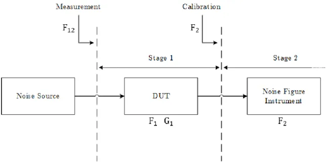
The equations of overall noise factor or overall noise temperature constrained to two stages are the basis for most noise figure measurement instruments. The following figure illustrates the noise figure measurement setup where the DUT is always labelled as Stage 1 and the instrumentation that follows is labelled as Stage 2.
Figure 12: Noise figure measurement setup.
2.2.1 Noise Power Linearity
In principle, the noise added by a DUT is the measured output noise power when a noiseless matched load is connected at its input [60]. However, in practice, a noiseless source cannot be obtained, so a different method must be used. A linear two-port device is characterized by an output noise power linearly dependent on the input noise power, which in turn is proportional to the temperature of the noise source, as it can be seen in the following figure.
The value of the internally generated noise of the DUT can be found if both the slope of the noise power characteristic and a reference point are known. This is the basis of the Y-factor method, which can be applied if two matched loads at significantly different temperatures are available [31]. The Y-factor technique is the most common method of measuring the quantities required by the cascaded noise formulas in order to calculate the noise factor 𝐹1 of the DUT [31, 34, 37].
2.2.2 Noise Source
A passive noise source may simply consist of a resistor held at a constant temperature while an active noise source may use a diode or transistor to provide a calibrated noise power output [60]. Figure 14 consists in the schematic of an active noise source.
Figure 14: Schematic of an active noise source [3].
A calibrated noise source is a device that provides two different levels of noise (hot and cold) and has a pre-calibrated Excess Noise Ratio (ENR) [3, 37], defined as 𝐸𝑁𝑅 =𝑇𝑆 𝑂𝑁− 𝑇 𝑆𝑂𝐹𝐹 𝑇0 (41)
where 𝑇𝑆𝑂𝑁 and 𝑇
𝑆𝑂𝐹𝐹 are the noise temperatures of the noise source in its on (hot)
and off (cold) states, and 𝑇0 is the reference temperature of 290 K. The calibrated ENR of a noise source is commonly expressed in decibel units [37].
2.2.3 Y-Factor Method
The Y-factor technique requires that the DUT is connected to one of two matched loads at different temperatures [37]. The noise slope can be determined by applying these two different levels of input noise and measure the output power change.
Figure 15: Representation of the Y-factor Method [31, 60].
In practice, the noise measurement instrument drives the noise source on and off to generate two temperature points, 𝑇𝑆𝑂𝑁 and 𝑇
𝑆𝑂𝐹𝐹, on the straight line 𝑘𝐺𝐵, and
measures the two power outputs of the DUT, 𝑃𝑂𝑁 and 𝑃𝑂𝐹𝐹, for these two temperatures [31]. The output noise power consists of noise power generated by the DUT as well as noise power from the noise source.
𝑃𝑂𝑁 = 𝐺𝑘𝑇𝑆𝑂𝑁𝐵 + 𝐺𝑘𝑇
𝑒𝐵 (42)
𝑃𝑂𝐹𝐹 = 𝐺𝑘𝑇𝑆𝑂𝐹𝐹𝐵 + 𝐺𝑘𝑇
𝑒𝐵 (43)
The Y-factor is the ratio of these two noise power levels and is measured by repeatedly pulsing the noise source on and off, so that an average value can be computed [34].
𝑌 = 𝑃𝑂𝑁
𝑃𝑂𝐹𝐹 (44)
Extrapolating the straight line to the 𝑇𝑆 = 0 point gives the noise added by the DUT, 𝑃𝐴𝐷𝐷. Hereupon, noise factor and effective input noise temperature may be obtained.
Additionally, from Equations 42, 43 and 44, the effective input noise temperature can be written in function of the source temperatures and the Y-factor as
𝑇𝑒 =
𝑇𝑆𝑂𝑁− 𝑌𝑇 𝑆𝑂𝐹𝐹
𝑌 − 1 (45)
The complete Y-factor measurement of a DUT noise factor and gain requires both calibration and measurement steps as already shown in Figure 12 to calculate all necessary quantities.
In this context, a noise measuring receiver of interest for this work is the radiometer due to its role in radio astronomy. This receiver and some additional radiometry concepts are covered in Appendix A.
2.3
Characteristics of a Two-Port Network
The behavior of a two-port network can be characterized by a set of scattering parameters, which are defined in terms of incident and reflected signals, and by a set of noise parameters characteristic of the device. The scattering parameters along with the impedance terminations of a two-port network may characterize a device
in terms of gain and mismatch while the noise parameters allow the evaluation of the noise performance of the device.
2.3.1 Scattering Parameters
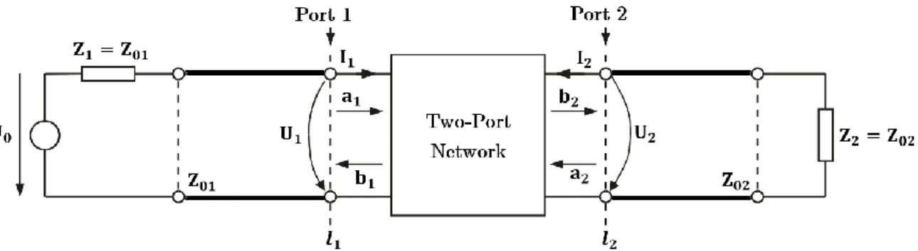
Figure 16 considers a two-port network where a generator with a source impedance 𝑍1 is placed at the input port and a load impedance 𝑍2 is connected to the output port.
Figure 16: General two-port network [40].
Dealing with wave propagation phenomena implies defining reference planes as 𝑙1 and 𝑙2 at the input and output ports, respectively. The quantities 𝑈𝑖 and 𝐼𝑖
stand for the total values of voltage and current, respectively, at the port 𝑖 = {1, 2}. In general, the normalized power waves are defined by
𝑎𝑖 = 𝑈𝑖+ 𝑍𝑖𝐼𝑖 2√|𝑅𝑒(𝑍𝑖)|
(46)
as the incident power wave and
𝑏𝑖 = 𝑈𝑖 − 𝑍𝑖
∗𝐼 𝑖
2√|𝑅𝑒(𝑍𝑖)|
(47)
as the reflected power wave. The dimension of these normalized equations is the square-root of power.
In general, both source and load impedances may be complex. However, the reference impedance 𝑍𝑖 is usually chosen to be real and equal to the characteristic impedance of the transmission line, 𝑍0𝑖, connected to the respective port 𝑖 [40]. A general two-port network taking into account the characteristic impedance of the transmission lines connected to the input and output port is represented in the following figure.
Figure 17: Practical case of a general two-port network.
The reflected power wave 𝑏𝑖 at any port 𝑖 will be composed by two components: the first results from the reflection of the incoming power wave 𝑎𝑖 at the same port 𝑖, while the second results from the transmission through the network of the incoming power wave 𝑎𝑗 (𝑗 ≠ 𝑖) at the other port. Thus, for a two-port network, it follows
𝑏1 = 𝑆11𝑎1+ 𝑆12𝑎2 (48)
𝑏2 = 𝑆21𝑎1+ 𝑆22𝑎2 (49)
The parameters 𝑆𝑗𝑖 are found by driving the port 𝑖 with an incident power wave 𝑎𝑖 and measuring the reflected power wave 𝑏𝑗 coming out of port 𝑗, while the
incident power wave 𝑎𝑗 on port 𝑗 is terminated in matched load to avoid reflections. Thus, 𝑆𝑖𝑖 is the reflection coefficient seen looking into port 𝑖 when port 𝑗 is terminated in matched load,
𝑆𝑖𝑖 = 𝑏𝑖 𝑎𝑖|𝑎
𝑗=0
, 𝑗 ≠ 𝑖 (50)
and 𝑆𝑗𝑖 is the transmission coefficient from port 𝑖 to port 𝑗 when port 𝑗 is terminated in matched load.
𝑆𝑗𝑖 = 𝑏𝑗 𝑎𝑖|𝑎
𝑗=0
, 𝑗 ≠ 𝑖 (51)
The frequency dependent parameters 𝑆11, 𝑆12, 𝑆21 and 𝑆22, which represent
reflection and transmission coefficients, are called the scattering parameters (or simply S parameters) of a two-port network, measured at specific locations at port 1 and 2 [23], and normalized to a specific reference impedance at each port.
Equations 48 and 49 can also assume a matrix form as [𝑏] = [𝑆][𝑎], and consequently this set of parameters can be represented as the scattering matrix
[𝑆] = [𝑆𝑆11 𝑆12
21 𝑆22] (52)
The scattering parameters imply a direct proportionality of outgoing and incoming power waves, which is a property of linear networks [40]. In the case of active networks, such as amplifiers, device characterization by scattering parameters depends on bias conditions and applies only for the small-signal regime [23].
2.3.2 Power Transport and Gain
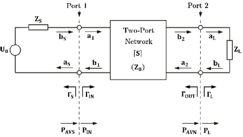
Several power gain equations can be defined when an arbitrary two-port network, characterized by its scattering matrix, is terminated by arbitrary source and arbitrary load impedances. The power transport from the source into the load through the two-port network arises different concepts of power, which are described by the scattering parameters of the general two-port network and the reflection coefficients at its ports, as shown in the following figure.
Figure 18: General two-port network with arbitrary source and load impedances.
The reflection coefficient seen looking toward the load is
Γ𝐿 =𝑍𝐿− 𝑍0
𝑍𝐿+ 𝑍0 (53)
while the reflection coefficient seen looking toward the source is
Γ𝑆 =
𝑍𝑆− 𝑍0
𝑍𝑆+ 𝑍0 (54)
where 𝑍0 is the characteristic impedance of the system.
The input impedance seen looking into port 1 of the two-port network when port 2 is terminated by 𝑍𝐿, is mismatched with a reflection coefficient given by
Γ𝐼𝑁 = 𝑆11+ 𝑆12𝑆21Γ𝐿
1 − 𝑆22Γ𝐿 (55)
while, similarly, the reflection coefficient seen looking into port 2 of the two-port network when port 1 is terminated by 𝑍𝑆 is
Γ𝑂𝑈𝑇 = 𝑆22+
𝑆12𝑆21Γ𝑆
The power dissipated by the load is given by the difference between the incident and reflected power,
𝑃𝐿 =
1
2|𝑏2|2− 1
2|𝑎2|2 (57)
Similarly, the power delivered to the input of the two-port network is
𝑃𝐼𝑁 =
1
2|𝑎1|2− 1
2|𝑏1|2 (58)
The power available from a source is defined as the power delivered by the source to a conjugate matched load. Thus, the power available from the source is given by
𝑃𝐴𝑉𝑆 = 𝑃𝐼𝑁(Γ𝐼𝑁 = Γ𝑆∗) (59)
The power available from the two-port network is the power delivered by the network to a conjugate matched load, that is
𝑃𝐴𝑉𝑁 = 𝑃𝐿(Γ𝐿 = Γ𝑂𝑈𝑇∗ ) (60)
Hereupon, the power gain definitions, which differ primarily in the way the source and the load are matched to the two-port device, can be defined. The operating power gain (or simply called power gain) is the ratio of the power dissipated in the load 𝑃𝐿 to the power delivered to the input of the two-port network 𝑃𝐼𝑁, and is independent of the source impedance 𝑍𝑆 [23, 60].
𝐺𝑃 =
1
1 − |Γ𝐼𝑁|2|𝑆21|2
1 − |Γ𝐿|2
|1 − 𝑆22Γ𝐿|2 (61)
The available power gain is the ratio of the power available from the two-port network 𝑃𝐴𝑉𝑁 to the power available from the source 𝑃𝐴𝑉𝑆, and depends on 𝑍𝑆,
𝐺𝐴 = 1 − |Γ𝑆|2
|1 − 𝑆11Γ𝑆|2|𝑆21|2
1
1 − |Γ𝑂𝑈𝑇|2 (62)
The transducer power gain is the ratio of the power delivered to the load 𝑃𝐿
to the power available from the source 𝑃𝐴𝑉𝑆 [23, 60]. It depends on both 𝑍𝐿 and 𝑍𝑆,
and therefore it usually appears as function of either the input reflection coefficient (Equation 55), 𝐺𝑇 = 1 − |Γ𝑆|2 |1 − Γ𝑆Γ𝐼𝑁|2|𝑆21| 2 1 − |Γ𝐿|2 |1 − 𝑆22Γ𝐿|2 (63)
or the output reflection coefficient (Equation 56),
𝐺𝑇 = 1 − |Γ𝑆|2
|1 − 𝑆11Γ𝑆|2|𝑆21|2
1 − |Γ𝐿|2
|1 − Γ𝐿Γ𝑂𝑈𝑇|2 (64)
The transducer power gain equation can also be defined in a different fashion without the numeric dependence of either input or output reflection coefficients [59], which consists in
𝐺𝑇 = (1 − |Γ𝑆|2)|𝑆21|2(1 − |Γ𝐿|2) |(1 − 𝑆11Γ𝑆)(1 − 𝑆22Γ𝐿) − 𝑆21𝑆12Γ𝑆Γ𝐿|2
(65)
Whenever conjugate matching is verified at both the input and output with respect to the two-port network, then the gain is maximized and 𝐺𝑃 = 𝐺𝐴 = 𝐺𝑇 holds. In contrast to conjugate matching, a special case occurs when both the input and output are matched for no reflection (Γ𝑆 = Γ𝐿 = 0 holds), and therefore the transducer power gain reduces to 𝐺𝑇 = |𝑆21|2. Another special case arises when 𝑆12
is negligibly small, which is true for several devices, and therefore the transducer power gain is defined as unilateral.
Hereupon, it is of interest to mention the definition of gain employed in the cascaded noise equations of section 2.1 was the available power gain.
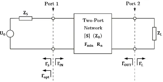
2.3.3 Noise Parameters
In terms of noise, an active two-port network, such as a transistor amplifier, is characterized by an equivalent noise resistance, 𝑅𝑁, and the minimum noise factor possible for the device, 𝐹𝑚𝑖𝑛, that is only achieved when a particular reflection coefficient, Γ𝑜𝑝𝑡, is presented to the input of the two-port network. The quantities
𝑅𝑁, 𝐹𝑚𝑖𝑛 and Γ𝑜𝑝𝑡 are characteristics of a particular transistor and are called the noise parameters of the device [23]. The noise parameters fully characterize the noise performance of a device for a specific set of conditions such as frequency, bias and temperature [59].
Thus, the noise factor of a noisy two-port network can be expressed as
𝐹 = 𝐹𝑚𝑖𝑛+
4𝑟𝑁|Γ𝑆− Γ𝑜𝑝𝑡|2
(1 − |Γ𝑆|2)|1 + Γ𝑜𝑝𝑡|2
(66)
where 𝑟𝑁 is the equivalent normalized noise resistance of the transistor (i.e. 𝑟𝑁= 𝑅𝑁/𝑍0) and Γ𝑆 is simply the source reflection coefficient. The following figure consists
of a two-port network described by its noise parameters.
Equation 66 describes the noise performance of a transistor, which is independent of the load termination and is determined solely by its source termination and noise parameters of the device.
The noise parameters of a device may be given by its manufacturer or measured and derived experimentally by varying the source reflection coefficient [59]. The minimum noise factor 𝐹𝑚𝑖𝑛 occurs when Γ𝑆 = Γ𝑜𝑝𝑡 and the rate at which the noise factor increases depends on the equivalent normalized noise resistance, 𝑟𝑁, which can be obtained by the noise factor value when the input is terminated by the characteristic impedance 𝑍0, as follows
𝑟𝑁 = (𝐹Γ𝑆=0− 𝐹𝑚𝑖𝑛)|1 + Γ𝑜𝑝𝑡|
2
4|Γ𝑜𝑝𝑡|2
(67)
2.4
Low-Noise Amplifier Design
In the design of any microwave transistor amplifier there are three distinct approaches according with the desired performance: high gain, low noise figure and high output power [16]. Appropriate matching networks set the specific performance of the transistor by establishing the required load and source impedances at the device ports. The stability of a transistor, or its resistance to oscillate, is also an important consideration in the design, and depends on the scattering parameters of the device, the matching networks and the respective terminations. The general circuit diagram used in the design of a microwave amplifier is represented in the figure below.
Figure 20: The general transistor amplifier circuit [40].
A LNA typically requires a compromise between gain and noise figure [22]. As long as the input signal power is low enough so that the device can be assumed to operate as a linear device, it is considered a small-signal amplifier. In the following sections stability is discussed along with the matching methods for maximum gain and low noise figure.
2.4.1 Stability Considerations
Oscillations are possible if either the input or output port impedances of a two-port network present a negative resistance, which occur when |Γ𝐼𝑁| > 1 or |Γ𝑂𝑈𝑇| > 1, respectively. Stability contemplates two cases: unconditional and
conditional stability. The first applies if |Γ𝐼𝑁| < 1 and |Γ𝑂𝑈𝑇| < 1 are satisfied for all
passive load and source impedances, i.e. |Γ𝐿| < 1 and |Γ𝑆| < 1. Thus, all passive
terminations provide a stable behavior for an unconditionally stable two-port network. The second applies if |Γ𝐼𝑁| < 1 and |Γ𝑂𝑈𝑇| < 1 are satisfied only for a certain range of passive load and source impedances. Thus, certain passive terminations may cause unstable behavior in a conditionally stable two-port network producing oscillations, and therefore this case is also referred to as potentially unstable.
The stability condition of an active two-port network is frequency dependent since the input and output matching networks generally depend on frequency as well as the scattering parameters of the device, which also depend on the bias conditions, and so a transistor is possible to be stable at its design frequency but unstable at other frequencies. An unconditional stable approach should require an unconditionally stable two-port network at all frequencies in order to guard against unexpected oscillations [59]. A conditional stable approach, however, requires extreme care to guarantee that a source or load termination that causes an oscillation is never presented to the device. This applies to all frequencies in-band and out-of-band.
Two-port stability is analyzed using either a graphical or numerical method [59]. The inequalities |Γ𝐼𝑁| < 1 and |Γ𝑂𝑈𝑇| < 1 define a range of values for Γ𝐿 and Γ𝑆
where the device will be stable. This range is established by stability circles plotted on a Smith chart that define the boundaries between stable and potentially unstable
regions of Γ𝐿 and Γ𝑆. The locus in the Γ𝐿 plane for which |Γ𝐼𝑁| = 1 is defined as the output stability circle with center
𝐶𝐿 =(𝑆22− Δ𝑆11∗ )∗ |𝑆22|2− |Δ|2 (68) and radius 𝑟𝐿 = | 𝑆12𝑆21 |𝑆22|2− |Δ|2| (69)
while the locus in the Γ𝑆 plane for which |Γ𝑂𝑈𝑇| = 1 is defined as the input stability circle with center
𝐶𝑆 = (𝑆11− Δ𝑆22∗ )∗ |𝑆11|2− |Δ|2 (70) and radius 𝑟𝑆 = | 𝑆12𝑆21 |𝑆11|2− |Δ|2| (71)
where Δ = 𝑆11𝑆22− 𝑆12𝑆21 is defined as the determinant of the scattering matrix. The stable region of the Smith chart is identified by checking if its center is a stable operating point, which means that all of the Smith chart that is exterior to the stability circle defines the stable region. On one hand, if |𝑆11| < 1 (|𝑆22| < 1)
when 𝑍𝐿 = 𝑍0 (𝑍𝑆 = 𝑍0) then |Γ𝐼𝑁| < 1 (|Γ𝑂𝑈𝑇| < 1) when Γ𝐿 = 0 (Γ𝑆 = 0) and the center of the Smith chart represents a stable operating point. On the other hand, if |𝑆11| > 1 (|𝑆22| > 1) when 𝑍𝐿 = 𝑍0 (𝑍𝑆 = 𝑍0) then |Γ𝐼𝑁| > 1 (|Γ𝑂𝑈𝑇| > 1) when Γ𝐿 =
0 (Γ𝑆 = 0) and the center of the Smith chart represents an unstable operating point.
Figure 21: Stable and unstable regions in the Γ𝐿 plane [23].
Figure 22: Stable and unstable regions in the Γ𝑆 plane [23].
Unconditional stability imposes the stability circles to fall completely outside (or totally enclose) the Smith chart for |𝑆11| < 1 (output stability circle) and |𝑆22| <
1 (input stability circle). Under these circumstances, the conditions for unconditional stability for all passive source and load impedances are expressed as ||𝐶𝐿| − 𝑟𝐿| > 1
and ||𝐶𝑆| − 𝑟𝑆| > 1 [23].
The scattering parameters of a device also allow a numerical analysis in order to conclude about its unconditional stability. A set of stability equations, in function of the two-port S parameters, may be defined as follows
𝐾 = 1 − |𝑆11|2− |𝑆22|2+ |Δ|2
![Figure 2: A typical radio telescope [53].](https://thumb-eu.123doks.com/thumbv2/123dok_br/15750857.1073653/29.892.251.667.498.765/figure-a-typical-radio-telescope.webp)