David Jorge Tiago Amoêdo
Licenciatura em Engenharia Eletrotécnica e de computadores
A 1.2 V Low Noise Amplifier with Double
Feedback for High Gain and Low Noise
Figure
Dissertação para obtenção do Grau de Mestre em Engenharia Eletrotécnica e de Computadores
Orientador: Prof. Doutor Luís Augusto Bica Gomes de
Oliveira, FCT-UNL
Júri:
Presidente: Prof. Doutor Paulo Miguel de Araújo Borges Montezuma de Carvalho, FCT/UNL
Arguente: Prof. Doutor João Pedro Abreu de Oliveira, FCT/UNL Vogal: Prof. Doutor Luís Augusto Bica Gomes de Oliveira,
A 1.2 V Low Noise Amplifier with Double Feedback for High Gain and Low Noise Figure
Copyright © David Jorge Tiago Amoêdo, Faculdade de Ciências e Tecnologia, Universidade Nova de Lisboa.
I dedicate this thesis to my family, mainly to my father Rui Amoêdo, to my mother Fernanda
Amoêdo, to my sister Catarina Amoêdo, to my grandmother Ercilia Mendes and all the rest of people
Acknowledgments
My first words are for my parents who always supported me, even when everything is not well.
After this, I would like to thank mainly to my leader professor Luis Augusto Bica Gomes de Oliveira
for all the advices, and support given while I was doing my project.
I would also like to thank to others professors such as: João Pedro Oliveira, Nuno Paulino,
Helena Fino, Rui Tavares and all others who supported me during the 6 years. I would like to thank to
my department of electrical and electronic engineering and the university Nova de Lisboa due to the
best conditions to work.
I have to thank to my colleagues Pedro Freitas, Pedro Raminhos, Tiago Vitorino, Vasco Ramos,
Mónica Lamas and António Fryxell for all support and help since I have started the course.
Related with the thesis, I would also like to thank to Fábio Querido, Hugo Serra, Nuno Pereira,
Universidade Nova de Lisboa
Abstract
Faculdade de Ciências e Tecnologia
Departamento de Engenharia Eletrotécnica e de Computadores
Mestrado Integrado em Engenharia Eletrotécnica e de Computadores
por David Jorge Tiago Amoêdo
In this thesis we present a balun low noise amplifier (LNA) in which the gain is boosted using a
double feedback structure. The circuit is based in a Balun LNA with noise and distortion cancellation.
The LNA is based in two basic stages: common-gate (CG) and common-source (CS). We propose to
replace the resistors by active loads, which have two inputs that will be used to provide the feedback
(in the CG and CS stages). This proposed methodology will boost the gain and reduce the NF (Noise
Figure). Simulation results, with a 130 nm CMOS technology, show that the gain is 19.65 dB and the
NF is less than 2.17 dB. The total power dissipation is only 5 mW (since no extra blocks are
Universidade Nova de Lisboa
Resumo
Faculdade de Ciências e Tecnologia
Departamento de Engenharia Eletrotécnica e de Computadores
Mestrado Integrado em Engenharia Eletrotécnica e de Computadores
por David Jorge Tiago Amoêdo
Nesta tese apresentamos um amplificador de baixo ruído (LNA), em que o ganho é aumentado
através de uma estrutura double feedback. O circuito é baseado num Balun LNA com cancelamento
de ruído e de distorção. O LNA é baseado em dois andares básicos: gate (CG) e
common-source (CS). Propomo-nos a substituir as resistências por cargas ativas, que têm duas entradas que
serão usados para fazer o feedback (nos andares CG e CS). Esta metodologia proposta vai aumentar o
ganho e reduzir a NF. Os resultados de simulação, com uma tecnologia CMOS de 130 nm, mostra que
o ganho é de 19,65 dB e o NF é inferior a 2,17 dB. A dissipação de energia total é de apenas 5 mW
(uma vez que não são necessários blocos adicionais), obtendo uma FOM de 3.13 mW-1 a partir de
Contents
Acknowledgments ... IV
Abstract ... V
Resumo ... VI
Contents ... VII
List of figures ... IX
List of tables... XI
Abbreviations ... XII
1 Introduction ... 1
1.1 Background and Motivation ... 1
1.2 Thesis Organization ... 2
1.3 Contributions ... 2
2 State-of-the Art Receiver Architectures and LNAs ... 4
2.1 Receivers Architectures ... 4
2.1.1 Heterodyne Receiver ... 4
2.1.2 Homodyne Receiver ... 6
2.1.3 Low-IF Receiver ... 10
2.2 Signal propagation ... 11
2.2.1 Impedance matching ... 11
2.2.2 Scattering Parameters ... 14
2.3 Low Noise Amplifiers... 15
2.3.1 Narrowband LNA’s... 16
2.3.2 Wideband LNA’s ... 17
2.3.3 Final remarks ... 20
3 Noise and Nonlinear distortion in LNAs ... 22
3.1 Noise ... 22
3.1.1 Thermal Noise ... 22
3.1.2 Flicker Noise ... 24
3.1.3 Noise Figure ... 24
3.2 Nonlinear Distortion ... 25
3.2.1 Harmonics ... 26
3.2.2 Intermodulation product ... 27
3.2.3 1 dB Compression Point ... 28
4 Common Gate and Common Source Stages ... 30
4.1 Common-Source Stage ... 30
4.1.1 Low frequency model neglecting 𝑟0 ... 31
4.1.2 Low frequency model with 𝑟0 ... 32
4.2 Common-Gate Stage ... 32
4.2.1 Low frequency model neglecting 𝑟0 ... 33
4.2.2 Low frequency model with 𝑟0 ... 35
5 Balun LNA with Noise Cancellation ... 38
5.1 Wideband Balun-LNA with Simultaneous Output Balancing, Noise-Canceling and Distortion-Canceling ... 38
5.1.1 Input Impedance ... 39
5.1.2 Gain ... 40
5.1.3 Noise factor ... 40
5.1.4 Circuit Implementation ... 41
5.2 MOSFET-Only Wideband Balun Low Noise Amplifier ... 41
5.3 A wideband inductorless LNA with local feedback and noise cancelling for low-power low-voltage applications ... 42
6 MOSFET-Only Low Noise Amplifier with Double Feedback ... 45
6.1 Theoretical Analyses ... 45
6.2 Simulations Results ... 47
6.3 Pre-Layout Simulations ... 51
6.4 Layout Design And Post-Layout Simulations ... 52
6.5 Discussion... 55
7 Conclusions and Future Work ... 57
7.1 Conclusions ... 57
7.2 Future Work ... 57
Published Paper ... 58
List of figures
Figure 2.1- Super-Heterodyne Receiver. ... 5
Figure 2.2 – Frequency spectrum showing the image signal adopted from [10]. ... 6
Figure 2.3 – Homodyne receiver: (a) single; (b) in quadrature adopted from [10]. ... 7
Figure 2.4 –DC offsets caused by “self-mixing”: (a) “LO leakage”; (b) interferer. ... 8
Figure 2.5 – Effect of I/Q mismatch in QPSK: (a) gain error, (b) phase error, (c) gain and phase error. ... 8
Figure 2.6 – Effect of even order distortion adopted from [10]. ... 9
Figure 2.7 – Image rejection architectures: (a) Hartley; (b) Weaver. ... 10
Figure 2.8 – Lumped circuit equivalent of a transmission line adopted from [10]. ... 12
Figure 2.9 – Schematic representation of a Two-Port Network with the incident and reflected waves. ... 15
Figure 2.10 – Common-source LNA with inductive degeneration adopted from [10]. ... 16
Figure 2.11 – Common-source stage with resistive input matching adopted from [10]. ... 17
Figure 2.12 – Common-gate LNA adopted from [10]. ... 18
Figure 2.13 – LNA with resistive shunt feedback: (a) schematic representation; (b) small signal model (low and medium frequencies) adopted from [9]. ... 19
Figure 3.1 – Models for thermal noise in a resistor adopted from [9]. ... 23
Figure 3.2 – Model for thermal noise in a MOSFET adopted from [10]. ... 23
Figure 3.3 – Noisy 2-port network with gain A adopted from [10]. ... 25
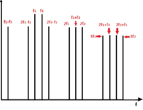
Figure 3.4 – Frequency spectrum showing the Intermodulation products of a 3rd order nonlinear device. ... 28
Figure 3.5 – Definition of the 1 dB compression point... 28
Figure 3.6 – Definition of IP3 adopted from [10]. ... 29
Figure 4.1 - Common-Source amplifier ... 30
Figure 4.2- Small-signal model of Common-Source amplifier neglecting 𝑟0 ... 31
Figure 4.3- Small-signal model of Common-Source amplifier with 𝑟0 ... 32
Figure 4.4- Common Gate stage ... 33
Figure 4.5- Common Gate stage small signal model for low frequencies ... 33
Figure 4.6- Input impedance ... 34
Figure 4.7- Small-signal model of Common-Gate stage with 𝑟0 ... 35
Figure 5.1- Balun LNA with noise canceling of CG-transistor adopted from [23] ... 39
Figure 5.2- MOSFET - Only LNA... 42
Figure 5.3- Previously proposed inductorless LNA’s: (A1) CS LNA with resistive feedback; (A2) CS LNA with active feedback; (B1) CG LNA with 𝑔𝑚 boosting; (B2) CG-CS LNA with noise cancelling adopted from [25]. ... 43
Figure 5.4 – Simplified schematic of the proposed LNA adopted from [25]. ... 43
Figure 5.5- Schematic representation of the relationship between 𝐴𝑉𝑀 and NF adopted from [25]. .. 44
Figure 6.1- MOSFET-Only LNA with Double Feedback ... 45
Figure 6.2- Comparison of Gain theoretical and simulated of LNA ... 48
Figure 6.3- Noise Figure of LNA... 48
Figure 6.4- Input impedance of LNA ... 49
Figure 6.5- MOSFET-Only LNA with Double Feedback IIP3 ... 50
Figure 6.6- Balun of MOSFET-Only LNA with Double Feedback ... 50
Figure 6.7- Gain of LNA ... 51
Figure 6.9- Input impedance of LNA ... 52
Figure 6.10- MOSFET-Only LNA layout (203.9 × 132.2 𝜇𝑚2)... 53
Figure 6.11- Layout of the total circuit with real current source, Balun and Pads (402.5 × 341.4 𝜇𝑚2). ... 53
Figure 6.12- Input impedance ( (a) Schematic, (b) Post-layout ) ... 54
Figure 6.13- Gain ( (a) Schematic, (b) Post-layout )... 54
List of tables
Table 1- MOSFET parameters ... 47
Abbreviations
AC
A
lternating
C
urrent
CG
C
ommon
G
ate
CMOS
C
omplementary
M
etal-
O
xide-
S
emiconductor
CS
C
ommon
S
ource
DC
D
irect
C
urrent
ISM
I
ndustrial
S
cientific and
M
edical
IIP
I
nput Referred
I
nterception
P
oint
GPS
G
lobal
P
osition
S
ystem
LNA
L
ow
N
oise
A
mplifier
LO
L
ocal
O
scillator
LOM
L
NA
O
scillator
M
ixer
NF
N
oise
F
actor
NMOS
N
channel
M
etal-
O
xide-
S
emiconductor
PMOS
P
channel
M
etal-
O
xide-
S
emiconductor
Q
Q
uality factor
RF
R
adio
F
requency
VCO
V
oltage
C
ontroller
O
scillator
FOM
F
igure
O
f
M
erit
ADC
A
nalog to
D
igital
C
onverter
DSP
D
igital
S
ignal
P
rocessor
SNR
S
ignal to
N
oise
R
atio
QPSK
Q
uadrature
P
hase-
S
hift
K
eying
BER
B
it
E
rror
R
ating
AM
A
mplitude
M
odulation
RC
R
adio
C
ontrolled
Chapter 1
1
Introduction
1.1
Background and Motivation
The technology and electronic devices have started to have a big impact in society. Many
companies had to develop and improve their systems, reducing cost and power consumption to can
compete in many fronts and in many economic markets. Several sectors of society such as medicine,
video games industry, telecommunications services and areas related with microchips and computers
were crucial for the growing of electronic, as well as all the techniques used to support that maturity.
The low voltage and low consumption electronic systems are needed and they are the
preferential demand in industry. This reality has more and more impact in all firms, workers and
mainly in the consumers around the world.
Nowadays, there is a high demand for wireless communications, which includes Industrial,
Scientific, and Medical (ISM) and Wireless Medical Telemetry Service (WMTS) applications [1].
These low cost applications require low power, low voltage transceivers fully integrated in a single
chip [2, 3]. The LNA that is a key block in these systems will be investigated in this thesis and they
may be divided into two groups: narrowband LNA and wideband LNA.
Narrowband LNAs use inductors and have very low noise figure, but they use a large area and
require a technology with RF options to have inductors with high Q.
Wideband LNAs with multiple narrowband inputs have low noise, but their design is very
complicated and the area and cost are high [2, 4].
RC LNAs are very simple wideband, but the conventional topologies have large noise figures.
Recently, wideband LNAs with noise and distortion cancelling [5] have been proposed, which may
have noise figures below 3 dB. Inductorless circuits have reduced die area and cost [6].
Wideband LNAs with high gain and low noise figure (NF), using noise and distortion
cancelation have been proposed [5-7]. But, these circuits have large power dissipation for high gain
and low noise figure.
In this thesis, the main goal is to design a very low area and low cost LNA, with very high
gain and low NF using a 1.2 V supply. This is obtained by replacing the load resistors by transistors
this thesis, is investigated the possibility of introduce a double feedback technique to boost the gain
and reduce the noise figure.
1.2
Thesis Organization
This thesis has been organized in six chapters, including this introduction.
In Chapter 2 are done some descriptions of the principal receiver’s topologies, as well as for
the principal receiver block, the LNA. After this, is described the existing LNA topologies, doing a
distinction between inductor and inductorless LNAs. Is also introduced the definitions, the basic
concepts and figures of merit, which are employed in LNAs.
In Chapter 3 is done a briefly description of the common-gate (CG) and the common-source
(CS) stages, which are used in the proposed LNA of this thesis.
In Chapter 4 is presented the LNA structure which combines the two amplifiers stages. The
principle of noise cancelation is explained and it is shown some different examples of this technique.
In Chapter 5 is investigated a Double Feedback structure, which is the proposed circuit in this
thesis. A theoretical analyses is made to obtain the equations of the circuit in order to optimize the
circuit. It is also shown the simulations results of the optimized design. The circuit layout is produced
and are shown the post-simulations results. Comparison with the state-of-the-art wideband LNAs is
made.
Finally, in Chapter 6 is given the overall conclusions and further research suggestions.
1.3
Contributions
For the complete LNA (combined CG and CS balun topology) is compared the conventional
design (with resistors) with the new MOSFET-Only with Double Feedback implementation optimized
for Gain and Noise Figure (NF).
In this work, equations of gain are presented, which can be used to optimize the circuit
performance. A circuit prototype in 130 nm standard CMOS technology at 1.2 V have been designed
and simulated to demonstrate the proposed technique. Finally, we are presented all the simulation
This work has originated the paper at the 4th Doctoral Conference on Computing, Electrical
and Industrial Systems (DoCEIS’13). It was developed directly related with the main goal of this
work entitled “A 1.2 V Low Noise Amplifier with Double Feedback for High Gain and Low Noise
Chapter 2
2
State-of-the Art Receiver Architectures and LNAs
In the present chapter, receiver architectures and the main RF (radio frequency) front-end
blocks are presented.
A transmitter, a receiver and a communication channel, in which the transmitted signals
propagate, are the key blocks of a communication system. In the case of wireless systems, the
information that is sent by the transmitter is included in a RF signal via a modulation process, i.e. by
varying at least one of the signal’s characteristics (amplitude, frequency or phase). Upon arrival at the receiver, the information needs to be recovered from the original RF signal through a demodulation
process. The communication medium, namely air (in the case of wireless communications), is not
ideal since the signals received are typically very weak (~ microvolts) and are susceptible to suffer interference from other, possibly stronger, signals. It is therefore important to be able to eliminate
undesired signals and isolate the signal of interest, so that it can be later amplified and converted to
baseband to go through demodulation, allowing the information contained in the signal to be
recovered.
2.1
Receivers Architectures
In order to carry more information in a signal, the signals are converted to high frequency for
transmission and then converted back for the baseband for reception. The size of the antenna is also
dependent on the frequency of the transmitted signal. Since the size is typically proportional to the
wavelength of the signal, the required antennas are smaller. Unfortunately, the influence of parasitics
(impedances, capacitors, etc.) is higher at high frequencies. The main receivers architectures
commonly used today are described below [2-8].
2.1.1
Heterodyne Receiver
The super-heterodyne receiver topology (Fig. 2.1), proposed by U.S. Army Major Edwin
Armstrong [9], is one of the most used architectures in wireless communication systems. The antenna
receives the RF signal which is filtered by a bandpass filter and subsequently amplified by a low noise
(mixer), having the output of a local oscillator (LO) applied to it. In order to isolate the desired signal
from signals present in adjacent channels, there is a bandpass filter at the desired frequency (IF),
called the channel selection filter, at the mixer output.
Figure 2.1- Super-Heterodyne Receiver.
Having IF, the desired RF frequency selected by tuning the LO, fixed is the major advantage
of this architecture, since designing the filter, which should be very selective and have a high quality
factor (Q), becomes much easier. Given that the process of demodulation takes place in the digital
domain, the introduction of an analog to digital converter (ADC) becomes necessary, followed by a
digital signal processor (DSP) to perform the demodulation process.
In order to gain a better understanding of the operation principle behind this receiver, namely
regarding the mixing, let us consider that at the mixer inputs there are the RF and LO signals, given
by
𝑣𝑟𝑓(𝑡) = 𝑉𝑟𝑓𝑐𝑜𝑠(𝜔𝑟𝑓𝑡) (2.1)
𝑣𝑙𝑜(𝑡) = 𝑉𝑙𝑜𝑐𝑜𝑠(𝜔𝑙𝑜𝑡) (2.2)
We obtain at the mixer output
𝑣𝑖𝑓(𝑡) = 𝑣𝑟𝑓(𝑡)𝑣𝑙𝑜(𝑡) =12 𝑉𝑟𝑓𝑉𝑙𝑜[𝑐𝑜𝑠 ((𝜔𝑟𝑓− 𝜔𝑙𝑜)𝑡) + 𝑐𝑜𝑠((𝜔𝑟𝑓+ 𝜔𝑙𝑜)𝑡)] (2.3)
The wanted signal is the one with the lower frequency so, from (2.3), the desired frequency,
given that 𝜔 = 2𝜋𝑓, is
𝜔𝑖𝑓 = 𝜔𝑟𝑓− 𝜔𝑙𝑜 (2.4)
In the presented example, the local oscillator frequency is smaller than the desired frequency
and this is called low-side injection. However, if the local oscillator frequency is higher, then it is
A bandpass filter, centered on the IF (𝑓𝑖𝑓), is used for channel selection, eliminating other unwanted signals that may appear in the spectrum. This process may present a challenge if, at the
mixer input, there is an image signal, i.e. a signal with frequency 𝑓𝑖𝑚 = 2𝑓𝑙𝑜− 𝑓𝑟𝑓 (Fig. 2.2). From this signal, after multiplication, two signals with frequencies 𝑓1= 𝑓𝑙𝑜− 𝑓𝑟𝑓 and 𝑓2= 3𝑓𝑜− 𝑓𝑟𝑓 are originated, 𝑓1 being coincident with 𝑓𝑖𝑓, overlapping the signal of interest and making it impossible to separate both signals. A filter, called image rejection filter, is therefore needed before the mixer to
prevent the interference of the image signal.
Figure 2.2 – Frequency spectrum showing the image signal adopted from [10].
The difference between the frequency of the RF and image signals is 2𝑓𝑖𝑓. Increasing 𝑓𝑖𝑓 allows for the image rejection filter specifications to be less strict but at the same time, with the
increase of 𝑓𝑖𝑓 the channel selection filter is required to have tighter specifications for the same bandwidth due to the increase of the quality factor 𝑄 = 𝑓0
∆𝑓. A compromise between intermediate
frequency and quality factor must be reached due to the difficulties present in the realization of filters
with high Q with CMOS technology. In practice, high performance filters must be realized externally,
rendering on chip full integration impractical.
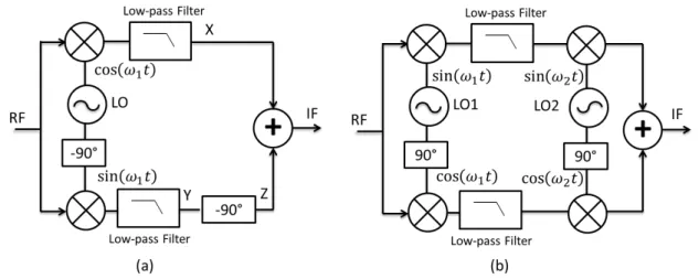
2.1.2
Homodyne Receiver
Given the problems associated with the integration of the heterodyne receiver, another
receiver topology, known as homodyne, direct conversion or “Zero-IF”, can be used. This type of receivers can work in direct conversion configuration (Fig. 2.3 (a)) or in quadrature conversion (Fig.
2.3 (b)).
In the direct conversion receiver, the RF signal is translated to the baseband in a single
filtered with a low-pass filter, which is simpler to design and integrate, in order to select the desired
channel [2-3]. Given that the signal and its image are separated by 2𝑓𝑖𝑓, this zero IF approach implies that the desired channel is its own image and therefore the image rejection filter is no longer required.
All the necessary processing is performed at the baseband and the requirements for the filters and
ADC’s are the more relaxed possible, favoring its integration [6].
Using modern modulation schemes, the signals are modulated in phase or frequency, which
differs from amplitude modulation (AM) where the sidebands have the same information, and the
down-conversion requires accurate quadrature signals [6]. Hence, in these cases, receivers with
quadrature down-conversion are used in order to ensure the preservation of the information contained
in the sidebands [10].
Figure 2.3 – Homodyne receiver: (a) single; (b) in quadrature adopted from [10].
Despite its simplicity, homodyne receivers present some drawbacks when compared with
heterodyne receivers, which hinder the use of this architecture in more demanding applications. These
disadvantages are explored below:
DC offsets – Given that the down-converted band extends down to zero frequency, the
presence of any offset voltage can corrupt the signal and saturate the receiver’s baseband output
stages. This problem can originate in leakages between the LO port and the LNA and mixer inputs if
the ports are not properly isolated, due to substrate and capacitive coupling. When a leakage signal
“LO leakage” appears at the inputs of LNA and mixer, the result of this “self-mixing” is a DC component at the mixer output which can lead to saturation of the following components (Fig. 2.4
(a)). Similar effects occur if the leakage comes from the LNA or mixer input to the LO port of the
Figure 2.4 –DC offsets caused by “self-mixing”: (a) “LO leakage”; (b) interferer.
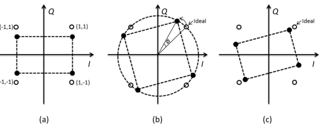
Quadrature error– When dealing with frequency or phase modulation, quadrature signals are
required, as explained earlier and ideally they should have the same amplitude and a phase shift of
90°. However, real circuits are not ideal and imbalances between I and Q appear, expressed as gain
and phase errors. The result of “I/Q mismatch” is the corruption of the down-converted signal constellation and a consequent increase of the bit error rate (BER). This is the most critical aspect of
these receivers, since modern wireless communication systems have different information in I and Q
and the implementation of accurate high frequency components with very accurate quadrature
relationship presents many challenges.
Figure 2.5 – Effect of I/Q mismatch in QPSK: (a) gain error, (b) phase error, (c) gain and phase error.
As example of the effect of I/Q mismatch on a Quadrature Phase-Shift Key (QPSK)
constellation in presented in Fig. 2.4. If the Q path in the mixer has smaller conversion gain than the
one for the I path, the Q signal will exhibit smaller amplitude than expected creating a gain error (Fig.
2.5(a)). Let us now assume that no gain error occurs but instead there is a phase error between the
signals fed by the LO to the splitter
𝑥𝐿𝑂,𝐼(𝑡) = 2 𝑐𝑜𝑠(𝜔0𝑡) (2.5)
𝑥𝐿𝑂,𝑄(𝑡) = 2 𝑐𝑜𝑠(𝜔0𝑡 + 𝜙) (2.6)1
If the RF signal provided by the LNA is given by 𝑥(𝑡) = 𝑎 𝑐𝑜𝑠(𝜔0𝑡) + 𝑏 𝑠𝑖𝑛(𝜔0𝑡), with a
and b equal to 1 or -1 to create the four constellation symbols, at the mixer output the following
signals are obtained
𝑦𝐼(𝑡) = 𝑎 + 𝑎 𝑐𝑜𝑠(2𝜔0𝑡) + 𝑏 𝑠𝑖𝑛(2𝜔0𝑡) (2.7)
𝑦𝑄(𝑡) = 𝑎 + 𝑎 𝑠𝑖𝑛(𝜙) + 𝑏 𝑐𝑜𝑠(𝜙) + 𝑎 𝑠𝑖𝑛(2𝜔0𝑡 + 𝜙) − 𝑏 𝑐𝑜𝑠(2𝜔0𝑡) (2.8)
which are then added and passed by a low-pass filter giving a resulting signal at baseband given by
𝑦(𝑡) = 𝑦𝐼(𝑡) + 𝑦𝑄(𝑡) = 𝑎 + 𝑎 𝑠𝑖𝑛(𝜙) + 𝑏 𝑐𝑜𝑠(𝜙) (2.9)
This result is directly related with the phase error illustrated in Fig. 2.5 (b). The combination
of gain and phase error is exemplified in Fig. 2.5 (c).
Even order distortion– if the LNA has a second order nonlinearity, such as 𝑦(𝑡) = 𝑎 𝑥(𝑡) +
𝑏 𝑥2(𝑡), and if near the channel of interest two interferers are present, 𝑥(𝑡) = 𝐴
1𝑐𝑜𝑠(𝜔1𝑡) +
𝐴2𝑐𝑜𝑠(𝜔2𝑡) are present, then one of the resulting output terms will be given by 𝑏 𝐴1𝐴2𝑐𝑜𝑠((𝜔1−
𝜔2)𝑡) and this shows that one of the interferer component is close to the baseband (𝜔1− 𝜔2). While in the case of ideal mixers this presents no problem, since this component becomes shifted to higher
frequencies after multiplication by the LO signal, in the case of real mixers some feedthrough directly
to the output will be present and part of the interferer will appear at the output at the baseband,
distorting the signal (Fig. 2.6).
In order to avoid this drawback, differential LNA’s and mixers are required to remove even
order harmonics. However, this implies higher power consumption and larger circuit areas.
Flicker noise – Another problem in this architecture is the presence of “flicker noise” that,
especially for MOSFET, is more relevant for low frequencies and it can substantially corrupt low
frequency baseband signals. This topic will be subject to further discussion in a subsequent section
dedicated to noise.
Despite its simplicity, this topology becomes impractical for certain applications, although
there are solutions to the problems stated above by adding additional complexity to the circuit.
2.1.3
Low-IF Receiver
The low-IF topology is a solution that combines features from both types of receivers,
heterodyne and homodyne, by using a mixed approach, i.e. by the selection of an intermediate
frequency. This choice of frequency allows for the specifications of the channel selection filter to be
relaxed while simultaneously avoids the problems related with direct conversion, especially the flicker
noise, which, as state above, has a strong impact in the baseband signal. The image cancelation, which
is a problem associated with heterodyne receivers, is achieved by using quadrature architectures, in
which the image is suppressed after the generation of a negative replica.
Image cancelation techniques were proposed by Hartley [11] and Weaver [12]. Note that
there are other architectures but we only speak about these two architectures.
Figure 2.7 – Image rejection architectures: (a) Hartley; (b) Weaver.
The Hartley architecture is represented in Fig. 2.7 (a). Let us assume that
𝑥𝑋(𝑡) =𝑉2 cos(𝑅𝐹 (𝜔𝑅𝐹− 𝜔𝐿𝑂)𝑡) +𝑉2 cos(𝐼𝑀 (𝜔𝐿𝑂− 𝜔𝐼𝑀)𝑡) (2.11)
𝑥𝑌(𝑡) = −𝑉2 sin(𝑅𝐹 (𝜔𝑅𝐹− 𝜔𝐿𝑂)𝑡) +𝑉2 sin(𝐼𝑀 (𝜔𝐿𝑂− 𝜔𝐼𝑀)𝑡) (2.12)
Given that 𝑠𝑖𝑛 (𝜃 −𝜋
2) = − 𝑐𝑜𝑠 𝜃, after a shift of -90°, at Z we obtain
𝑥𝑍(𝑡) =𝑉𝑅𝐹2 cos((𝜔𝑅𝐹− 𝜔𝐿𝑂)𝑡) −𝑉2 cos(𝐼𝑀 (𝜔𝐿𝑂− 𝜔𝐼𝑀)𝑡) (2.13)
In the last step of this procedure, the signals xX and xZ are added allowing the recovering of the desired signal while at the same time canceling the image component.
The Weaver architecture (Fig. 2.7(b)) is similar to the Hartley architecture, except the -90°
phase shift in one of the signal paths is replaced by a second mixing operation in both signal paths,
which has the same effect as the -90° phase shift used in Hartley’s configuration. Direct conversion to the baseband can be achieved by adequately selecting the second LO frequency.
Despite the fact that both architectures of low-IF topology, Hartley and Weaver, are
susceptible to I/Q mismatch which may lead to incomplete image rejection, it is still a flexible
compromise between heterodyne and Zero-IF topologies.
2.2
Signal propagation
2.2.1
Impedance matching
In circuits that use high frequencies, the wavelengths tend to be of the same order of
magnitude as the physical dimensions of the circuit. Therefore, lumped circuit analysis, which
assumes nearly instantaneous signal propagation (𝑙𝑐𝑖𝑟𝑐𝑢𝑖𝑡 ≪ 𝜆), is not appropriate. In this scenario, circuit paths behave like transmission lines, which require distributed parameters analysis.
A segment of a transmission line can be represented by an equivalent lumped circuit (Fig. 2.8)
Figure 2.8 – Lumped circuit equivalent of a transmission line adopted from [10].
The resistance R represents the conductor loss while the conductance G is related to the
dielectric loss between the two conductors. Given that we can represent the system as an equivalent
lumped circuit, the Kirchhoff’s voltage and current laws are applicable and we obtain
𝑣(𝑧, 𝑡) − 𝑅Δ𝑧 𝑖(𝑧, 𝑡) − 𝐿Δ𝑧 𝜕𝑖(𝑧, 𝑡)𝜕𝑡 − 𝑣(𝑧 + Δ𝑧, 𝑡) = 0 (2.14)
𝑖(𝑧, 𝑡) − 𝐺Δ𝑧 𝑣(𝑧 + Δ𝑧, 𝑡) − 𝐶Δ𝑧𝜕𝑣(𝑧 + Δ𝑧, 𝑡)
𝜕𝑡 − 𝑖(𝑧 + Δ𝑧, 𝑡) = 0
(2.15)
Dividing both equations by Δ𝑧, taking the limit for Δ𝑧 → 0 and keeping in mind that the definition for the derivate of a function 𝑓 is given by 𝑓′(𝑎) = 𝑙𝑖𝑚
𝛥𝑥→0
𝑓(𝑎+𝛥𝑥)−𝑓(𝑎)
𝛥𝑥 , the result gives:
𝜕𝑣(𝑧, 𝑡)
𝜕𝑧 = −𝑅 𝑖(𝑧, 𝑡) − 𝐿
𝜕𝑖(𝑧, 𝑡)
𝜕𝑡 (2.16)
𝜕𝑖(𝑧, 𝑡)
𝜕𝑧 = −𝐺 𝑣(𝑧, 𝑡) − 𝐶
𝜕𝑣(𝑧, 𝑡)
𝜕𝑡 (2.17)
Particularly, in the sinusoidal steady-state condition, the equations above can be simplified to
yield
𝑑𝑉(𝑧)
𝑑𝑧 = −(𝑅 + 𝑗𝜔𝐿)𝐼(𝑧) (2.18) 𝑑𝐼(𝑧)
𝑑𝑧 = −(𝐺 + 𝑗𝜔𝐶)𝑉(𝑧) (2.19)
Upon application of derivative in both terms of equations (2.16) and (2.17) the following
second order differential equations are obtained:
𝑑2𝑉(𝑧)
𝑑2𝐼(𝑧)
𝑑𝑧2 − 𝛾2𝐼(𝑧) = 0 (2.21) where,
𝛾 = √(𝑅 + 𝑗𝜔𝐿)(𝐺 + 𝑗𝜔𝐶) (2.22)
is the propagation constant, which is dependent on frequency. Solving the differential equations above
it is possible to obtain the following expressions for the current and voltage of the traveling waves in
any specific point of the transmission line:
𝑉(𝑧) = 𝑉0+𝑒−𝛾𝑧+ 𝑉0−𝑒𝛾𝑧 (2.23)
𝐼(𝑧) = 𝐼0+𝑒−𝛾𝑧+ 𝐼0−𝑒𝛾𝑧 (2.24)
where the wave propagation in the +z and –z directions is given by the terms 𝑒−𝛾𝑧 and 𝑒𝛾𝑧 respectively. Applying the simplified equation obtained for the sinusoidal steady-state (2.18) on
equation (2.23) the following expression for the current over the line will be give by
𝐼(𝑧) = (𝑉0+𝑒−𝛾𝑧− 𝑉0−𝑒𝛾𝑧)𝑅 + 𝑗𝜔𝐿𝛾 (2.25)
Given that the obtained result must be equivalent to (2.24) we conclude that 𝐼0+= 𝑉0+ 𝛾 𝑅+𝑗𝜔𝐿
and 𝐼0−= 𝑉0− 𝛾
𝑅+𝑗𝜔𝐿 and define the transmission line characteristic impedance, 𝑍0, as
𝑍0 =𝑉0 +
𝐼0+ =
𝑉0−
𝐼0− =
𝑅 + 𝑗𝜔𝐿
𝛾 (2.26)
If the line is terminated by a load 𝑍𝐿 at 𝑧 = 0 (Fig. 2.8), assuming that the source of the wave is located at a position 𝑧 < 0, the following condition must be verified
𝑍𝐿=𝑉(0)𝐼(0) =𝑉0 ++ 𝑉
0−
𝑉0+− 𝑉 0−𝑍0
(2.27)
where 𝑉0+ and 𝑉0−are the amplitude voltages of the incident and reflected waves respectively. The voltage reflection coefficient, Γ, which is the amplitude of the reflected wave normalized to the incident wave amplitude, can be derived from the previous equation
Γ =𝑉𝑉0−
0+=
𝑍𝐿− 𝑍0
𝑍𝐿+ 𝑍0 (2.28)
characteristic impedance. Usually in RF the characteristic impedance of an antenna is 50 Ω, so the first block of a receiver must have the input impedance matched to the same value.
2.2.2
Scattering Parameters
Traditional system characterization used in low-frequencies trough open and short-circuit
measurements is not possible at high frequencies, since the current and voltage measurements involve
the magnitude and phase of the travelling wave [18]. Therefore, at high frequencies, since the device
length is no longer negligible relatively to the wavelength of the travelling waves, network
characterization must be done through different parameters. The scattering parameters, or
S-parameters, relate the voltages of the incident and reflected waves, at n-ports, through the scattering
matrix,
[𝑉1
−
⋮ 𝑉𝑛−
] = [𝑆11⋮ ⋯ 𝑆1𝑛⋮ 𝑆𝑛1 ⋯ 𝑆𝑛𝑛
] [𝑉1
+
⋮ 𝑉𝑛+
] (2.29)
where 𝑉𝑖 is the voltage amplitude on port 𝑖 and the signal, + or -, relates to the incident and reflected wave, respectively. To determine a specific s-parameter, the following expression is used
𝑆𝑖𝑗 =𝑉𝑖 −
𝑉𝑗+|
𝑉𝑘+≠0,𝑘≠𝑗
(2.30)
This means that an s-parameter 𝑆𝑖𝑗 is determined as the ratio between the reflected wave voltage at port I and the incident wave at port j, when the other ports are terminated with a matched
load so that reflections are avoided. These parameters can be measured directly using a network
analyzer, which allows an accurate network characterization without the need to know every detail of
the circuit inside the network.
In the specific case of a two-port network, the s-parameters can be designated according to
their physical meaning as follows [13]:
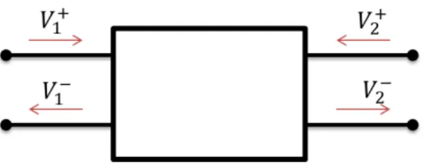
Figure 2.9 – Schematic representation of a Two-Port Network with the incident and reflected waves.
The s-parameters are particular important in receiver front-ends, since they are helpful in
LNA design, due to the need of input matching, and are also associated with the concept of return
loss, which is a figure of merit for signal reflection, indicating the fraction of the incident power that
is reflected back to the source. The input return loss is usually included in LNA’s technical
specifications and is defined as
𝑅𝐿 = −20 𝑙𝑜𝑔(|𝑠11|) (2.31)
Naturally, the aim is to minimize the reflected power, so that more power is transferred to the
load. Usually, designers aim for at least 10 dB return loss, meaning that only a maximum of 10% of
the total power is reflected back to the source.
2.3
Low Noise Amplifiers
The low noise amplifier (LNA) is an electronic amplifier used to amplify weak signals, that
can be, regarding bandwidth, narrowband, multi-band or wideband [14-15]. It is typically used as the
first stage of amplification. In order to maximize the power transfer, the LNA input impedance should
be matched with the antenna’s characteristic impedance. The LNA must provide enough gain for the
desired SNR while simultaneously keeping a low noise factor to minimize the introduction of noise in
the system. To accomplish the above requirements in a system consisting of several blocks connected
in cascade, further considerations are needed. The overall noise factor of a cascade of stages is given
by Friis equation [16] which can be written as:
𝐹 = 𝐹1+𝐹2𝐺− 1 1 +
𝐹3− 1
𝐺1𝐺2 + ⋯ +
𝐹𝑛− 1
𝐺1𝐺2… 𝐺𝑛−1 (2.32)
where 𝐹𝑛 and 𝐺𝑛 are the noise factor and the available power gain of the 𝑛𝑡ℎ stage, respectively. From (2.32), it is clear that the noise factor of the first stage, i.e. of the LNA, is the dominant term and that
if its gain is high enough it will significantly reduce the noise contribution of the subsequent stages.
The overall performance of stages in a cascade, regarding linearity, can be characterized by
1 𝐼𝐼𝑃3=
1 𝐼𝐼𝑃3,1+
𝐺1
𝐼𝐼𝑃3,2+
𝐺1𝐺2
𝐼𝐼𝑃3,3+ ⋯ (2.33)
with 𝐼𝐼𝑃3,𝑖 and 𝐺𝑖 being the third-order intercept point (input referred) and the power gain of the 𝑖𝑡ℎ stage, respectively. The overall system linearity is limited by the performance of the stage with the
worst 𝐼𝐼𝑃3.
The 𝐼𝐼𝑃3 of the last stage is directly related to the gain of the preceding stages, but at the same time a high gain for the first stage is necessary for a low noise figure. Therefore, there must be a
compromise between noise and linearity.
2.3.1
Narrowband LNA’s
Common-source LNA with degeneration
One of the most used topologies to design a narrowband LNA is the common-source (CS)
LNA with inductive degeneration (Fig. 2.10) since this topology allows a low noise figure, high gain
and easy input matching.
Figure 2.10 – Common-source LNA with inductive degeneration adopted from [10].
The input impedance of the CS LNA is given by
𝑍𝑖𝑛 = 𝑠(𝐿𝑔+ 𝐿𝑠) +𝑠𝐶1 𝑔𝑠+
𝑔𝑚
where the inductances, 𝐿𝑔 and 𝐿𝑠, are chosen so that they resonate with the device capacitance 𝐶𝑔𝑠 at the frequency of operation which is expressed as
𝜔0 = 1
√(𝐿𝑔+ 𝐿𝑠)𝐶𝑔𝑠
(2.35)
This allows the elimination of the imaginary component of 𝑍𝑖𝑛 and matches the term 𝑔𝑚 𝐶𝑔𝑠𝐿𝑠 to
50 Ω. Given that the gain of the device is proportional to 𝑔𝑚, the inductance 𝐿𝑔 introduces some freedom in the design of the LNA. One of the advantages of this configuration is the improvement of
the noise factor due to the use of inductors, which are ideally noiseless. However, their use increases
significantly the die area of the LNA which, combined with RF options (thick metal layer for high Q
inductors), lead to an increase of the production costs.
2.3.2
Wideband LNA’s
Common-source with resistive input matching
Resistive input matching is one the simplest ways to obtain a stable input impedance. This
technique, which is employed in the CS stage (Fig. 2.11), uses a resistor in parallel with the amplifier
input.
Figure 2.11 – Common-source stage with resistive input matching adopted from [10].
Unfortunately, the use of a resistor is associated with the introduction of a significant amount
Let us assume that the amplifier has an available power gain 𝐴𝑝 and a noise power at output,
𝑃𝑛 due to internal sources only. If the source has an impedance 𝑅𝑠, the noise factor can be computed using equation (2.37) and yields the following result
𝐹 =4𝑘𝐵𝑇𝑅𝑆𝐴𝑃4𝑘+ 4𝑘𝐵𝑇𝑅𝑖𝑛𝐴𝑃+ 𝑃𝑛
𝐵𝑇𝑅𝑆𝐴𝑝 = 2 +
𝑃𝑛
4𝑘𝐵𝑇𝑅𝑠𝐴𝑝 (2.36)
to which a noise figure of at least 3 dB (𝑁𝐹 ≥ 3 𝑑𝐵) is associated.
Common-gate
One of the most widely used topologies in the implementation of LNA’s is the common gate topology (Fig. 2.12). One of the reasons for this fact is that it has an intrinsic wideband response.
In a first order approximation, the input impedance is given by 1
𝑔𝑚, and 𝑔𝑚 can be dimensioned easily in order to obtain the input impedance matching.
Figure 2.12 – Common-gate LNA adopted from [10].
The lower bound of the noise factor can be estimated considering only the transistor thermal
noise level. If it is input referred, the noise factor can be written as
defining 𝛼 as 𝑔𝑚
𝑔𝑑0. As stated earlier, for long channel devices the noise excess factor, 𝛾, is 2
3 and
short-channel effects can be neglected (𝛼 = 1) [21] with matching 𝑔𝑚𝑅𝑆= 1. The minimum noise factor can then be estimated to be approximately 𝐹 =5
3, which corresponds to 𝑁𝐹 ≈ 2.2 𝑑𝐵. However, since
𝑔𝑚 is imposed by the matching condition, the gain is only dependent on the load 𝑍𝐿 and, while increasing 𝑍𝐿 causes an increase in gain, it will also generate increased levels of noise. The possible gain being, therefore, limited.
In practice, the noise figures for a CG-LNA are above 3 dB.
LNA with resistive shunt feedback
In Fig. 2.13 (a), it is shown a wideband LNA using the feedback resistor 𝑅𝑆 for matching. According to the incremental model depicted in Fig. 2.13 (b) the input impedance can be expressed as
𝑍𝑖𝑛=𝑠𝐶 𝑅𝐹+ 𝑍𝐿
𝑔𝑠(𝑅𝐹+ 𝑍𝐿) + 1 + 𝑔𝑚𝑍𝐿= (
1 𝑠𝐶𝑔𝑠//
𝑅𝐹+ 𝑍𝐿
1 + 𝑔𝑚𝑍𝐿) (2.38)
Figure 2.13 – LNA with resistive shunt feedback: (a) schematic representation; (b) small signal model (low and medium frequencies) adopted from [9].
Given that the previous equation is dependent on many variables, some assumptions need to
impedance can be simply written as 1
𝑔𝑚. Analogously, using similar reasoning for the low frequency
case, the gain is then written as
𝐴𝑣=(1 − 𝑔𝑅 𝑚𝑅𝐹)𝑍𝐿 𝐹+ 𝑍𝐿
(2.39)
and if the load 𝑍𝐿 is high then 𝑔𝑚𝑅𝐹≫ 1 and the gain is the simplified into
𝐴𝑣 ≈ −𝑔𝑚𝑅𝐹 (2.40)
This approximation is very useful regarding the noise factor [17], which can be expressed as
𝐹 = 1 +𝑅𝑅𝐹
𝑆(
1 + 𝑔𝑚𝑅𝑆
1 − 𝑔𝑚𝑅𝐹) 2
+𝑅1
𝑠𝑍𝐿(
𝑅𝐹+ 𝑅𝑆
1 − 𝑔𝑚𝑅𝐹) 2
+𝛾𝑔𝛼𝑅𝑚
𝑠 (
𝑅𝐹+ 𝑅𝑆
1 − 𝑔𝑚𝑅𝐹) 2
(2.41)
Analyzing the equation above, it is clear that increasing the term 𝑔𝑚𝑅𝐹 the noise factor is reduced and the gain enhanced, as expected. 𝑔𝑚 is set by the matching condition, so 𝑅𝐹 is the parameter available that can be increased. In this situation, the previous assumption to have a high load 𝑍𝐿 comparatively to 𝑅𝐹 is no longer valid. Hence, in order to achieve optimal performance, 𝑅𝐹 and 𝑔𝑚 need to be carefully dimensioned.
2.3.3
Final remarks
In the previous sections, basic LNA architectures were presented in the single-ended form.
However, a differential structure may be used instead. In order to perform the transformation from the
antenna into a differential signal, a balun would be required, which would introduce extra losses and
additional noise in the system.
As we know the narrowband LNAs present good noise figure, high gain, and accurate
matching due to the LC tuning for the frequency of interest, but inductors occupy a large area and
increase significantly the cost of the chip.
The wideband LNAs are typically inductorless, suitable for systems with low area and with
non-critical specifications. With the scaling of CMOS technology it is possible to achieve low power,
low cost, and an acceptable noise figure, and inductorless wideband LNAs became a competitive
choice to implement multi-band LNAs. These can be implemented by using narrowband LNAs in a
Narrowband LNA:
Good noise figure
High gain
Accurate matching due to the LC tuning for the frequency of interest
Large area associated to the inductors
Significant increase in chip cost
Wideband LNA:
Suitable for systems with low area and non-critical specifications
Due to scaling of CMOS technology it is possible to achieve:
Low power
Low cost
Chapter 3
3
Noise and Nonlinear distortion in LNAs
3.1
Noise
Noise, in electronics, manifests as a random fluctuation in an electrical signal and is
characteristic of all electronic circuits. It manifests itself as a random variable that can be introduced
by physical phenomena related with the nature of the materials or by external interferences. Noise has
a non-deterministic nature and its instantaneous value is not predictable being, therefore, impossible
to eliminate a priori.
Given that noise is present in every electronic circuit, it is important to analyze it carefully
and then we need to develop methods to help minimize its effects.
In the following section, the main sources of noise present in CMOS transistors are presented
and described [14-4].
3.1.1
Thermal Noise
Thermal noise, also known as Johnson-Nyquist noise, is the electronic noise generated by the
thermal agitation of the charge carriers (typically electrons) inside an electrical conductor at
equilibrium causing a variation in current, which is present regardless of the applied voltage. The
thermal noise power is proportional to the temperature (absolute) and can be quantified by:
𝑃 = 𝑘𝐵𝑇𝛥𝑓 (3.1)
where 𝑘𝐵is Boltzmann’s constant and Δf represents the bandwidth of the system. The average noise power generated in a resistor is given by
𝑉𝑡ℎ2
̅̅̅̅
̅̅̅̅ = 4𝑘𝐵𝑇𝑅∆𝑓 (3.2)
and can be modeled using an ideal resistor (noise free) in series with a voltage source or in parallel
with a current source, both of which are responsible for the introduction of noise in the model (Fig.
Figure 3.1 – Models for thermal noise in a resistor adopted from [9].
Figure 3.2 – Model for thermal noise in a MOSFET adopted from [10].
In the case of MOS transistors, carrier motion through the channel is also a source of thermal
noise which can be represented by a current source in parallel with the conducting channel (Fig. 3.2).
If the transistor is operating in the triode region, the noise generated in the channel is given by
[19]:
𝐼̅ = 4𝑘𝑛2 𝐵𝑇𝛾𝑔𝑑0∆𝑓 (3.3)
where gd0 is the channel conductance at zero drain-source voltage and γ is the noise excess factor (NEF) which is equal to 1 for this bias condition (𝑉𝐷𝑆= 0). This result can be extended to long-channel MOSFET devices operating in saturation [20]:
𝐼̅ = 4𝑘𝑛2 𝐵𝑇𝛾𝑔𝑚∆𝑓 (3.4)
3.1.2
Flicker Noise
Flicker noise is also often referred to as 1/𝑓 noise or pink noise (even though both terms have wider definitions) due to its 1/𝑓 or pink power density spectrum.
In FET’s, it originates in a somewhat unpredictable physical phenomenon which is related
with the interface between the gate oxide and the silicon substrate (SiO2/Si). This type of noise is
associated with fluctuations in the number of carriers in the channel due to trapping and release of the
carriers in the SiO2/Si. Due to its 1/𝑓 dependence, flicker noise becomes dominant at low frequencies.
An adequate model for its representation consists of a voltage source in series with the gate, expressed
as
𝑉𝑛𝑓2
̅̅̅̅̅ = 𝑘𝑓
𝑐𝑜𝑥𝑊𝐿𝑓𝑎𝑓 (3.5)
with 𝑘𝑓 being a process dependent and bias independent constant, 𝑐𝑜𝑥 being the gate oxide capacitance per unit area and 𝑊 and 𝐿 the width and length of the MOSFET respectively. The values of 𝑘𝑓 vary depending on the quality of the fabrication process, being lower for cleaner fabrication processes. 𝑘𝑓 is also lower in p-channel devices, when comparing the value to the one for n-channel devices, flicker noise being therefore more relevant in the latter case. The exponent 𝑎𝑓 is close to 1 but can vary between 0.7 and 1.2 [20]. This type of noise is still under study regarding its origin and
modeling.
3.1.3
Noise Figure
The noise figure (NF) and the noise factor (F) are measures of the degradation of the signal-to
noise ratio (SNR) and serve as a number by which the performance of a radio receiver can be
specified.
Considering a circuit characterized by a 2-port network, the noise factor is defined as the ratio
between the total noise power at the 2-port output and the 2-port output noise power due to the input
noise sources only and is given by:
𝐹 =𝑂𝑢𝑡𝑝𝑢𝑡 𝑛𝑜𝑖𝑠𝑒 𝑑𝑢𝑒 𝑡𝑜 𝑡ℎ𝑒 𝑠𝑜𝑢𝑟𝑐𝑒𝑇𝑜𝑡𝑎𝑙 𝑜𝑢𝑡𝑝𝑢𝑡 𝑛𝑜𝑖𝑠𝑒 𝑝𝑜𝑤𝑒𝑟 (3.6)
The noise figure is simply the noise factor expressed in decibels (dB), i.e. NF can be
𝑁𝐹 = 10 𝑙𝑜𝑔 𝐹 (3.7)
Figure 3.3 – Noisy 2-port network with gain A adopted from [10].
As an example, let us consider a noisy 2-port network represented in Fig. 3.3. The noise
factor is given by
𝐹 =𝐴𝑁2𝑁2
1 (3.8)
with 𝑁1 and 𝑁2 being the noise power available at the 2-port input and output, respectively.
If the ports are adapted and a power signal S1 is applied from the generator, then according to
the power transfer theorem, the signal must be completely transferred to the 2-port and so is the signal
power signal S2 from the 2-port output to the load resistor 𝑅𝐿. The power gain is then given by
𝐴2 =𝑆2
𝑆1 . (3.9)
Replacing in eq. (3.8), the noise factor can then be written as
𝐹 = 𝑆1
𝑁1
𝑆2
𝑁2
=(𝑆/𝑁)(𝑆/𝑁)𝑖
𝑜 . (3.10)
The previous equation relates the noise factor with the SNR’s at the input and output of the 2 -port, showing the degradation of the SNR caused by the 2-port. If no additional noise is introduced by
the 2-port the value of F should be unity (𝐹 = 1).
3.2
Nonlinear Distortion
Nonlinear distortion is a term used to describe the phenomenon of non-linearity between the
compression point and the 3rd-order intermodulation product, both of these parameters appearing in
the systems’ specifications.
A linear system generates an output signal proportional to the input signal. However, for
many devices, a linear model is only applicable for small signals. Most devices have non-linear
characteristic, and if they are memoryless and time invariant, the input-output relationship may be
represented by a polynomial or Taylor series, i.e.
𝑦 = ∑ 𝑎𝑖𝑥𝑖 𝑛
𝑖=0
= 𝑎0+ 𝑎1𝑥 + ⋯ + 𝑎𝑛𝑥𝑛 (3.11)
The type of non-linearity is directly related to the terms used in the description of these
devices, its representation being more accurate if more terms are used.
3.2.1
Harmonics
Nonlinear devices generate harmonics. Characterizing a nonlinear device by a 3rd-order
polynomial is typically a good approximation and it allows simplification to be done in the
calculations. Let us assume sinusoidal input signal given by
𝑣𝑖(𝑡) = 𝑉𝑚𝑐𝑜𝑠(𝜔𝑓𝑡) . (3.12)
Therefore the output will be expressed as
𝑦(𝑡) = 𝑎0+ 𝑎1𝑉𝑚𝑐𝑜𝑠(𝜔𝑓𝑡) + 𝑎2𝑉𝑚2𝑐𝑜𝑠2(𝜔𝑓𝑡) + 𝑎3𝑉𝑚3𝑐𝑜𝑠3(𝜔𝑓𝑡) (3.13)
Taking into account the trigonometric relations 𝑐𝑜𝑠2𝑥 =1+𝑐𝑜𝑠 2𝑥
2 and 𝑐𝑜𝑠3𝑥 =
3 𝑐𝑜𝑠 𝑥+𝑐𝑜𝑠 3𝑥 4 , equation (3.14) can be rewritten as
𝑦(𝑡) = 𝑎0+ 𝑎2𝑉𝑚2
2 ⏟ 𝐷𝐶 𝑐𝑜𝑚𝑝𝑜𝑛𝑒𝑛𝑡
+ (𝑎1𝑉𝑚+ 3𝑎3𝑉𝑚3
4 ) cos(𝜔𝑓𝑡) ⏟ 1𝑠𝑡𝐻𝑎𝑟𝑚𝑜𝑛𝑖𝑐 (𝑓𝑢𝑛𝑑𝑎𝑚𝑒𝑛𝑡𝑎𝑙)
+ 𝑎2𝑉𝑚2
2 cos(𝜔𝑓𝑡) ⏟ 2𝑛𝑑 𝐻𝑎𝑟𝑚𝑜𝑛𝑖𝑐
+ 𝑎3𝑉𝑚3
4 cos(𝜔𝑓𝑡) ⏟ 3𝑟𝑑𝐻𝑎𝑟𝑚𝑜𝑛𝑖𝑐 (3.14)
An n-order nonlinearity will generate n harmonics, each with a frequency that is multiple of
3.2.2
Intermodulation product
Let us assume that instead of applying a single sinusoidal signal at the non-linear input, two
signals with different frequencies, 𝜔1 and 𝜔2, are now applied. The input signal can then be written as
𝑣𝑖(𝑡) = 𝑉1cos(𝜔1𝑡) + 𝑉2cos(𝜔2𝑡) (3.15)
Intermodulation between both frequencies will generate additional signals that are not simply
harmonic frequencies (multiples of each frequency), but also sum and difference frequencies of the
input signal frequencies and multiples of those sum and difference frequencies, i.e. Intermodulation
products appear at frequencies 𝑛𝜔1± 𝑚𝜔2.
For the considered input, given by equation (3.15), the Intermodulation products generated at
the output are given by
𝑦(𝑡)
= 𝑎0+ 𝑎1(𝑉1cos(𝜔1𝑡) 𝑉2cos(𝜔2𝑡))
+ 𝑎2[
𝑉12
2 (1 + cos(2𝜔1𝑡)) + 𝑉22
2 (1 + cos(2𝜔2𝑡)) + 𝑉1𝑉2(cos((𝜔1+ 𝜔2)𝑡) + cos((𝜔1− 𝜔2)𝑡))
]
+ 𝑎3
[
(34 𝑉13+32 𝑉1𝑉22) cos(𝜔1𝑡) + (34 𝑉23+32 𝑉2𝑉12) cos(𝜔2𝑡) +
3
4𝑉12𝑉2(cos((2𝜔1+ 𝜔2)𝑡) + cos((2𝜔1− 𝜔2)𝑡)) + 3
4 𝑉22𝑉1(cos((2𝜔2+ 𝜔1)𝑡) + cos((2𝜔2− 𝜔1)𝑡)) + 3
4 𝑉13cos(3𝜔1𝑡) + 3
4 𝑉23cos(3𝜔2𝑡) ]
(3.16)
The appearance of the different frequencies is illustrated in Fig. 3.4 for the particular case of a
Figure 3.4 – Frequency spectrum showing the Intermodulation products of a 3rd order nonlinear device.
3.2.3
1 dB Compression Point
The 1 dB compression point is a linearity measure of a circuit and it specifies the output
signal power that is lower than the nominal output of the ideal (linear) circuit by 1 dB (Fig. 3.5).
Past this point, the saturation is reached and consequently degrades the signal. A linear
system is out of its normal operation mode if it is operating above 𝑃1𝑑𝐵.
3.2.4
Third-order intercept point
The third-order intercept point (IP3) is defined as the interception between the curves of the
power output of the fundamental frequency and the third-order intermodulation product (IM3) if both
these curves were linear, i.e. when the amplitude for both is the same. In order to determine the
intercept point, a practical rule consists in using the position of the 1 dB compression point as a
starting point, since the 1 dB compression point should fall 10dB below the intercept point. The
specification of the IP3 is usually input-referred (IIP3), but it can also be output-referred (OIP3). An
example of the latter is illustrated in Fig. 3.6.
Chapter 4
4
Common Gate and Common Source Stages
4.1
Common-Source Stage
Common-Source amplifier (Fig. 4.1) is one of the basic single-stage amplifiers, typically used
as transconductance impedance or a voltage. This stage has the main objective high input and output
impedances and high voltage gain. Note that this stage is not good for a single stage wideband LNA
[21].
Figure 4.1 - Common-Source amplifier
Now, by analyzing the small-signal model, equations are going to be derived for the gain in
two different ways. First we are going to start with the simplest transistor model, where we neglected
4.1.1
Low frequency model neglecting
𝑟
0In this stage, the input signal is going to be injected to the gate, which is isolated from the
transistor channel, thus for low frequencies the input impedance is considered infinite. Note that the
bulk and the source are connected to the ground, which means that there is no body effect.
Figure 4.2- Small-signal model of Common-Source amplifier neglecting 𝑟0
Gain
By analyzing the small-signal model shown in Fig. 4.2 we obtain
𝑉𝑜𝑢𝑡 = −𝑔𝑚. 𝑉𝑖𝑛. 𝑅𝐷 (4.1)
𝑉𝑉𝑜𝑢𝑡
𝑖𝑛 = −𝑔𝑚. 𝑅𝐷 (4.2)
4.1.2
Low frequency model with
𝑟
0Figure 4.3- Small-signal model of Common-Source amplifier with 𝑟0
Gain
By analyzing the circuit on Fig. 4.3 we can see that 𝑟0 is in parallel with the load resistor, 𝑅𝐷, and therefore, the gain is given by
𝐴𝑣𝐶𝑆= −𝑔𝑚.𝑟𝑟0. 𝑅𝐷
0+ 𝑅𝐷 . (4.4)
4.2
Common-Gate Stage
The common gate stage (Fig. 4.4) is a known amplifier topology that will be used as one of
the stages in the proposed LNA. A theoretical analysis will be shown to obtain the key parameters
(input matching, gain and noise) and two types of approximation are performed.
Now, we are going to review some expressions for input impedance, gain, and noise. For each
Figure 4.4- Common Gate stage
4.2.1
Low frequency model neglecting
𝑟
0In Fig. 4.5 is represented the common gate stage small signal model for low frequencies. For
simplify, the output impedance of the transistor is neglected. As the signal, 𝑉𝑖𝑛, is applied in
transistor’s source terminal, we have to consider the body effect, represented in the model by a voltage controlled current source which depends on source-bulk voltage, 𝑉𝑠𝑏.
Gain
Using the small-signals analyses it is possible to obtain the gain. At output, the signal is given
by
𝑉𝑜𝑢𝑡= 𝑅𝐷. 𝑖 . (4.5)
For this case 𝑉𝑠𝑏= −𝑉𝑔𝑠 = 𝑉𝑖𝑛, and the expression in order to express the current 𝑖 is
𝑖 = 𝑔𝑚𝑏. 𝑉𝑠𝑏− 𝑔𝑚. 𝑉𝑔𝑠 (4.6)
𝑖 = 𝑉𝑖𝑛. (𝑔𝑚+ 𝑔𝑚𝑏) (4.7)
After this, we can obtain the CG gain, substituting on (4.5)
𝐴𝑣𝐶𝐺 =𝑉𝑉𝑜𝑢𝑡
𝑖𝑛 = 𝑅𝐷. (𝑔𝑚+ 𝑔𝑚𝑏). (4.8)
Input Impedance
Using the scheme of Fig. 4.6, it was possible to show the expression for the input impedance,
which is viewed from the source.
Figure 4.6- Input impedance
𝑖 = −𝑉𝑔𝑠. (𝑔𝑚− 𝑔𝑚𝑏) (4.9)
𝑖 = 𝑉𝑖𝑛. (𝑔𝑚+ 𝑔𝑚𝑏) (4.10)
and the input impedance is given by
𝑍𝑖𝑛𝐶𝐺=𝑔 1
𝑚+ 𝑔𝑚𝑏 (4.11)
4.2.2
Low frequency model with
𝑟
0In previous section (4.2.1.), in order to simplify, it was considered that 𝑟0 (transistor output impedance) was infinite. Now, in this section we are going to derive the same expressions, but considering the value of 𝑟0.
In Fig. 4.7 we can see the 𝑟0 is modeled with a resistor between the source and the drain of the transistor.
Gain
Analyzing the small-signals, it is possible to obtain the gain. We can see that the current
flowing in 𝑅𝑆 is the same that goes for 𝑅𝐷, so
𝑉𝑜𝑢𝑡 = 𝑅𝐷. 𝑖 (4.12)
𝑉𝑜𝑢𝑡
𝑅𝐷 = 𝑖 (4.13)
and the current 𝑖𝑟0 is given by
𝑖𝑟0 =𝑉𝑅𝑜𝑢𝑡
𝐷 + 𝑉𝑔𝑠. (𝑔𝑚+ 𝑔𝑚𝑏). (4.14)
As we know,
𝑉𝑔𝑠= 𝑅𝑆. 𝑖 − 𝑉𝑆 (4.15)
And replacing (4.13), we obtain
𝑉𝑔𝑠= 𝑅𝑆.𝑉𝑅𝑜𝑢𝑡
𝐷 − 𝑉𝑆 (4.16)
In terms of Kirchhoff's Voltage Law (KVL), we can expressed the output voltage (𝑉𝑜𝑢𝑡) as,
𝑉𝑜𝑢𝑡= 𝑉𝑆− 𝑅𝑆. 𝑖 − 𝑟0. 𝑖𝑟0 (4.17)
𝑉𝑜𝑢𝑡
𝑉𝑆 =
𝑅𝐷. (1 + 𝑟0. (𝑔𝑚+ 𝑔𝑚𝑏))
𝑅𝐷+ 𝑟0+ 𝑅𝑆. (1 + 𝑟0. (𝑔𝑚+ 𝑔𝑚𝑏)) = 𝐴𝑣 . (4.18)
Finally, assuming 𝑅𝑆= 0, the gain of CG stage is given by
𝐴𝑣𝐶𝐺=𝑅𝐷. (1 + 𝑟𝑅0. (𝑔𝑚+ 𝑔𝑚𝑏))
Input Impedance
Analyzing Fig. 4.6, the input voltage is given by the sum of drop voltages in 𝑟0 and 𝑅𝐷, in other words,
𝑉𝑖𝑛= 𝑟0. 𝑖𝑟0+ 𝑅𝐷. 𝑖 (4.20) and as we know,
𝑖𝑟0 = 𝑖 + 𝑉𝑔𝑠. (𝑔𝑚+ 𝑔𝑚𝑏) (4.21)
Now, we can replace (3.21) on (3.20), where 𝑉𝑔𝑠= −𝑉𝑖𝑛 and the input impedance is given by
𝑍𝑖𝑛𝐶𝐺 =𝑣𝑖𝑖𝑛 (4.22)
𝑍𝑖𝑛𝐶𝐺 =𝑟 𝑟0+ 𝑅𝐷
![Figure 2.3 – Homodyne receiver: (a) single; (b) in quadrature adopted from [10].](https://thumb-eu.123doks.com/thumbv2/123dok_br/16583346.738663/19.892.133.759.417.670/figure-homodyne-receiver-single-b-quadrature-adopted.webp)
![Figure 2.6 – Effect of even order distortion adopted from [10].](https://thumb-eu.123doks.com/thumbv2/123dok_br/16583346.738663/21.892.190.707.804.1101/figure-effect-order-distortion-adopted.webp)
![Figure 2.8 – Lumped circuit equivalent of a transmission line adopted from [10].](https://thumb-eu.123doks.com/thumbv2/123dok_br/16583346.738663/24.892.174.721.134.317/figure-lumped-circuit-equivalent-transmission-line-adopted.webp)
![Figure 2.11 – Common-source stage with resistive input matching adopted from [10].](https://thumb-eu.123doks.com/thumbv2/123dok_br/16583346.738663/29.892.360.525.748.1016/figure-common-source-stage-resistive-input-matching-adopted.webp)
![Figure 2.13 – LNA with resistive shunt feedback: (a) schematic representation; (b) small signal model (low and medium frequencies) adopted from [9]](https://thumb-eu.123doks.com/thumbv2/123dok_br/16583346.738663/31.892.192.710.579.962/figure-resistive-feedback-schematic-representation-signal-frequencies-adopted.webp)
![Figure 3.3 – Noisy 2-port network with gain A adopted from [10].](https://thumb-eu.123doks.com/thumbv2/123dok_br/16583346.738663/37.892.185.706.118.350/figure-noisy-port-network-gain-adopted.webp)