ISSN 1546-9239
© 2008 Science Publications
Corresponding Author: Somayeh Timarchi, Faculty of Electrical and Computer Engineering, Shahid Beheshti University, Tehran, Iran, Tel: +98 21 29902286, Fax: +98 21 2417940, E-mail: [email protected]
Low Power Modulo 2
n+1 Adder Based on Carry Save Diminished-One Number System
Somayeh Timarchi, Omid Kavehei, and Keivan Navi
Department of Electrical and Computer Engineering,
Shahid Beheshti University, Tehran, Iran
Abstract: Modulo 2n+1 adders find great applicability in several applications including RNS implementations. This paper presents a new number system called Carry Save Diminished-one for modulo 2n+1 addition and a novel addition algorithm for its operands. In this paper, we also present a novel architectures for designing modulo 2n+1 adders, based on parallel-prefix carry computation units. CMOS implementations reveal the superiority of the resulting adders against previously reported solutions in terms of implementation area and delay.
Keywords: Modulo 2n+1 addition, carry save diminished-one number system, parallel-prefix adders, residue number system, computer arithmetic, VLSI circuits.
INTRODUCTION
The Residue Number System (RNS) is a non-weighted number system [1] that can map large numbers to smaller residues, without any need for carry propagations [2]. Arithmetic operations like addition, subtraction and multiplication can be performed on residue digits concurrently and independently. Thus, using residue arithmetic, would in principle, increase the speed of computations [3, 4, 5].
RNS has shown high efficiency in realizing special purpose applications such as digital filters [6, 7, 8,
9], image processing [10], RSA cryptography [11] and
specific applications for which only additions, subtractions and multiplications are used and the number dynamic range is specific.
Special moduli sets have been used extensively to reduce the hardware complexity in the implementation of converters and arithmetic operations [12, 13]. Among which the triple moduli set
{
2n−1 , 2 , 2n n+1}
have somebenefits [14]. Because of operand lengths of these moduli, the operation delay is determined by the modulo 2n +1 channel. Therefore, the design of efficient modulo 2n +1 adders is critical [15]. Modulo 2n +1 operations are used in many applications such as DSP algorithms[16], Fermat Number Transform for elimination of round off errors in convolution computations[17, 18, 19], cryptography[20] and in pseudorandom number generation[21]. Modulo 2n +1 adders are also utilized as the last stage adder of modulo 2n +1 multipliers.
In the last few years, several algorithms and architectures have been proposed for designing modulo
2n+1 adders . These algorithms are based on two number systems :
• To overcome the problem of (n+1)-bit wide circuits for the modulo 2n +1 channel, the diminished-one number system [17] has been proposed. In this system, efficient adders have been reported in [14, 22
-25]
. But these adders need a special treatment for zero operands.
For this problem, a new number representation called “Carry Save Diminished-one” (CSD-1) is proposed in this paper. With this system, the addition with zero operand doesn’t need a special treatment, which reduces the adder chip area.
• Modulo 2n +1 adders can be designed as a special case of general modulo m adders. The most efficient circuits for generalized modulo adders are reported in [15, 26-28]. In [15], the proposed adder is more efficient than the ones proposed by [26-28]. However, the corresponding structure [15] uses a 3-operand adder which is eliminated in our method. In the paper, we derive a new methodology for modulo 2n +1 adder that leads to a parallel-prefix adder architecture. Using implementation in a CMOS technology, we show that the pro posed parallel-prefix design methodology uses considerably less chip area than that reported in [23] (diminished-one number system) and less chip area and propagation delay than the approach reported in [15] (normal number system).
FOUNDATION Modulo 2n
A = Ah2n + Al.
A mod (2n +1) = (Ah2n + Al) mod (2n +1) = (Al -Ah) mod (2n +1).
Therefore, the reduction modulo 2n +1 is computed by subtracting the high n-bit word from the low n-bit word and then conditionally adding 2n +1 if the subtraction yields a negative result.
Diminished-One Number System: In the diminished-one number system, the number A is represented by
1
A′ = −A and the value zero is treated separately, i.e., it requires an additional zero indication bit. In this system, the ordinary addition can be implemented by an end-around-carry parallel-prefix adder with
c
in=
c
out[17, 25]
:
S' = (S-1) = (A+B-1) mod (2n+1) = [(A'+1) + (B'+1) - 1)] mod (2n+1) = (A' + B' + 1) mod (2n+1)
= (A' + B' +
c
out) mod 2n (1)Algorithm 1: (Modulo 2n +1 addeition in diminished-1 number system): A number in diminished-one is represented by n+1 bits in which the (n+1)th bit is used to indicate ‘0’. In [17], the modulo 2n +1 addition algorithm has been presented for zero and non zero operands:
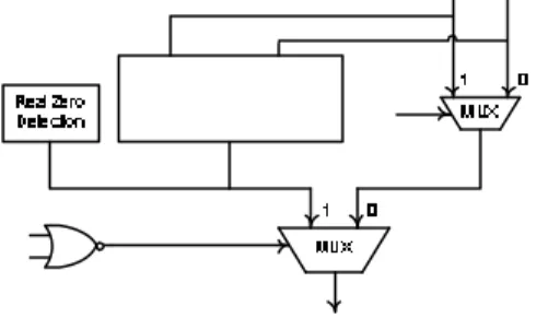
1) If the most significant bit of one addend is ‘1’, inhibit the addition and the other addend is the sum (Fig. 1).
2) If the msb of both addends are ‘0’, ignore the msb, add the n lsb’s, complement the carry and add it to the n lsb’s of the sum.
The modulo 2n +1 adder in Fig. 1 can be designed in different ways. To increase the modulo addition speed, the delay of carry computation should be minimized. In many papers, parallel-prefix adders have been proposed for this purpose.
) 0 , 1 (n−
B A(n−1,0)
) 0 , (n A
) 0 , (n B
) 0 , 1 ( 1n−
O O2(n,0)
) 0 , (n S
) ( 1n O
) (n A
) (n B
) (n A
(
)
Adder Modulo 2n+1Fig. 1: The general design of diminished-one modulo adder
Parallel-Prefix Adders: Parallel-prefix adders are usually used in papers for speeding up the addition operation. They minimize the carry computation time. In the prefix technique, n inputs x0 . . . xn-2 xn-1 and an
arbitrary associative operator are used to compute n
outputs
0
1 x
x x
yi= io i− oLo for i = 0, n-1. Thus, each
output yi depends on all inputs xj of same or lower range
(j= i). In a binary addition, the carry propagation is a prefix problem.
Prefix structures can be represented by using a direct acyclic graph. The
o
operator on a pair of (g pi, i) terms is usually represented by a node and a carry computation unit is represented as a tree structured interconnection of such nodes. Several tree structures have been proposed in [29, 30].THE NEW CSD-1 NUMBER S YSTEM AND ITS MODULO
2
n+
1
ADDITION ALGORITHM
CSD-1 Number System: In the proposed method, we try to improve the performance of modulo 2n +1 arithmetic units by using a carry save coding. Table 1 shows the new representation of numbers.
Table 1: The CSD-1 coding for modulo 2n +1
Range Bit Representation
[0 , 2n] ˜ . . . ˜˜
˜
As shown in table 1, this representation is composed of n positions (digits), with two bits in the first position and n-1 bits in other ones. A number X is represented as below:
X = xn-1 . . . x2 x1 x'0
x ?0
We call this system “carry save diminished-one”. If
(
)
0 0
X ≠ X = then x′0=1
(
x0′=
0)
. When we eliminate this bit from representation, the remaining bits are equal to diminished-one representation of X. Also there are two bits in the first position; therefore we have a carry save representation. So we call this system “Carry Save Diminished-one” (CSD-1).CSD-1 is extendable to any other modulo when diminished-one is only defined for modulo 2n +1.
CSD-1 Addition Algorithm: In this section, we present the CSD-1 addition algorithm for modulo 2n +1 (Algorithm 2).
Algorithm 2: (CSD-1 addition): This algorithm is decomposed into 2 steps.
Step 1. The first step is based on the following theorem:
Theorem 1: Let A and B be two CSD-1 numb ers in the range [0, 2n+1]. Then,
− +
< − + +
− + =
+ +
otherwise B
A
B A if B
A B
A
n n n n
n
2 2 2 1
2
1
2 1 1
1
Proof:
( )
(
)
(
)
− − +
< − + +
− + =
+ − +
+ < + +
=
+ +
otherwise B
A
B A if B
A
otherwise B
A
B A if B
A B A
n
n n
n
n
2 1
2 1 1
1 1 2
1 2 1
2
(2)
When n
B
A+ −1<2 then
(
A+B−1)
+1= A+B−12n +1 (3)The maximal value of (3) is 2n. In CSD-1, this value can be represented by (n+1) bits in n positions. In other words, the output carry resulting from
2
1 n 1
A B+ − + is 0. Thus, the term (3) is transformed into:
n n
n A B
B A
2 2
2 1 1 1
1 + = + − +
− +
Since A, B∈[0, 2n], the second case of equation (2) leads to the following inequalities:
n n n n n
B
A+ −1−2 ≤2 +2 −1−2 < 2
So,
2 2
1 2 1 2 n 1 n
n n
A+ − − = + − −B A B = + −A B
Therefore, from (2) we get:
− +
< − + +
− + =
+ +
otherwise B
A
B A if B
A B
A
n n n
n
2 2
1 2
1
2 1 1
1
(4)
Y The equation (4) outlines the impact of the output carry of (A+B-1). In the CSD-1 number system, this carry is produced when the sum is larger than 2n. The carry generation indicates that the sum is equal or greater than the modulo. Let assume Cout is the output carry of (A+B-1). Thus the carry of (A+B-1) will be generated when:
(
)
'1' 1 2 1 2 2
2 1
n n
out
n
c A B A B
A B
= ⇔ + − ≥ + ⇔ + ≥ +
⇔ + > +
(5) Thus, if the sum of two numbers is greater than the modulo, the output carry of (A+B-1) is ‘1’ and the sum is correct according to theorem 1: there is no need to increment the result.
The output carry is zero in the following cases:
(
)
( )
( )
' 0 ' 1 2 1
2 1 *
2 1
2 1 **
n out
n n
n
c A B
A B A B
A B
= ⇔ + − < +
+ < +
⇔ + ≤ +
+ = +
(6)
In condition (*), since A+B is less than the modulo, the output carry of (A+B-1) is ‘0’. According to equation (4), the sum should be incremented in the second stage. Therefore from (4), (5) and (*) we have:
if A B+ < +2n 1 or 2n 1
A+ > +B then:
(
)
mod 2(
n 1)
(
1)
outS= A+B + = A+ − +B c (7) But in condition (**) of equation (6), when
2n 1
A+ = +B , equation (7) leads to S =1, which is not true. To correct this case, we introduce step 2 of Algorithm 2 that will be presented later.
In our method, (A+B-1) is computed without any extra hardware and only by ignoring a0′ in above sum. As mentioned earlier, if A≠0thena0′ =1; thus (A+B-1) will be achieved by eliminating
a
0′
. IfA
=
0
then A+B will be computed by removinga
0′
. In this case, we have always cout =' 0 ' and the sum will be incremented according to equation (7). But incrementing shouldn’t be done to obtain the correct result.The first step of Algorithm 2 reveals that a two-stage combinational circuit is required for modulo addition (adder and incrementer). The first stage computes an intermediate sum M.
(
)
(
)
0
0
1 0 0
0 1
M A B if A a
M A B if A a
′
= + − ≠ =
′
= + = =
Therefore, we adjust equation (7) as below:
(
)
mod 2(
1)
0n
out
A+B + = +M c +a′ (8)
M in equation (8) is achieved by addition of A and B excludinga0′. The range of M is given by theorem 2.
Proof: If A=0 then M=A+B=B. Since B
∈
[0, 2n] then the theorem is established. The situation is the same if B=0.If A≠0and B ? 0 then
M
= + −
A
B
1
. Since,
2
n1,
0
A B
< +
A
>
and B > 0 then,1
2 0
1 ) 1 2 ( ) 1 2 ( 1
0< + − < n+ + n+ − ⇔ < ≤ n+
M B
A
(9) The maximal value of M is 2n+1 which can be presented by n+2 bits or n+1 digits in CSD-1 (for this maximal value, all bits are ‘1’). Y
In the second stage, the least n posibits of M is incremented according to (8).
Step 2 : As described before, if A+B ≠2n +1then theorem 1 leads to equation (8). But if A+B =2n +1
then the correct output of S=0 should be produced. In this case, A and B are non zero and
1 2n
M = + − =A B .
According to theorem 2 and equation (8), if the msb of M, mn=0(Cout = 0) then M should be incremented in the second stage. Thus the final output is 2n+1. In CSD-1, each numb er is in the range of [0, 2n] and can be represented by n digits. Therefore the output carry can be ignored and the output sum is “0…01” that can be corrected by inverting
s
0′
.In the second step of Algorithm 2, we introduce two methods to detect zero output and to correct it. a) The correct output zero occurs when two inputs are
complementary, i.e. their sum is equal to modulo 2n+1. One method to recognize complementary numbers is the logical AND of the outputs of ai XOR bi (for any i except i = 0). A similar method has been mentioned in [23].
b) Another method is based on the following theorem. Theorem 3: (Complementary of two inputs): Two inputs are complementary when (and only when) the input and output carries of the incrementer are ‘1’. Proof:
o First, we prove that if A and B are complementary
numbers, the input and output carries of the incrementer are ‘1’. When A and B are complementary, both of them are non zero.
Therefore, 1 (2n 1) 1 2n
M = + − =A B + − = . In
CSD-1, 2n has n digits. Thus, cout = ⇒0 cout =1. The input carry of the incrementer is
1 . 0
* =c a′ =
cin out .
The output carry of the incrementer is equivalent to the output carry of the following addition:
(
+ −1)
+1= + =2 +1= A B A B n
S
Obviously, the output carry is ‘1’.
o Now we prove that if input and output carries of
the incrementer are ‘1’ then A and B are complementary numbers.
If * 1 in
c = then 0
(cout.a′ =) 1. Therefore
A
≠
1
andcout=0. In other words, M = + −A B 1 and we have:1 2n 2n 1
M= + − ≤ ⇒ + ≤ +A B A B (10) The output carry of the incrementer is ‘1’ when the sum is equal or more than 2n+1. That is:
(
A+ − + ≥B 1)
1 2n+ ⇒ + ≥ +1 A B 2n 1 (11) Equations (10) and (11) are simultaneous verif ied when A+B = 2n+1, which shows that A and B are complementary.Y Method (a) has been used in [23]. However the method (b) for zero detection and correction consumes less area than method (a). Then, we implemented method (b). As described earlier and according to example 1,
s
0′
can be transformed to ‘0’ in the condition of zero detection.THE PROPOSEH CSD-1 P ARALLEL-PREFIX ADDER (CSD-PP)
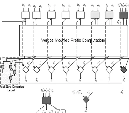
One way for implementing the CSD-PP adder is based on the adder architecture of Fig. 2. But instead of having a dedicated single stage for reentering the carry,
[23]
has proposed to perform carry recirculation at each existing prefix level. Then, there is no need for the extra carry increment stage. As a result, a dedicated CSD-PP adder architecture is derived with one less prefix level compared to those derived from Fig. 2 architecture. In the CSD-1 system, it requires several modifications. These modifications will be introduced by the 3 following theorems.
Theorem 4: Let assume that
( )
G P, =( )
G,P and, a b
G
andP
a b, , with a > b, are respectively the group generate and propagate signals for the group a, a-1, a-2, ... , b-1, b, computed by:In our case, in which the reentering carry is given by the expression
a G
0′
n−1, the carriesc
*i of the addition modulo 2n+1 are equal to Gi*, where Gi* is computed by the prefix equations:(
* *)
(
(
1)
1(
)
)
0 1, 1 1, 1
, 1
,
, , 0 2
n n
i i
i i n i n i
G P i
G P
G P a G P if i n
− − − + − + = − = ′ ⋅ ≤ ≤ − o Proof:
(
)
(
)
(
)
(
)
(
)
(
)
(
)
(
)
(
)
(
)
(
)
(
)
(
1, 1 0 1, 1)
1 , 1 0 1 , 1 1 , 1 0 1 , 1 1 0 1 , 1 0 1 , 1 1 0 1 , 1 0 1 , 1 1 , 1 1 0 1 , 1 1 , 1 1 0 1 , 1 1 , 1 1 0 1 * * , , , , , , , , , , , + − + − + − + − + − + − − + − + − − + − + − + − − + − + − − + − + − − − ′ ⋅ = ′ ⋅ + = ′ ⋅ + = ′ ⋅ + ′ ⋅ + = ′ ⋅ + ′ ⋅ + = ′ ⋅ + + = ′ ⋅ ⋅ + + = ′ ⋅ = i n i n i i i n i n i i i n i i n i i n i i n i i n i i n i i n i i n i n i i n i i n i n i i n i i n i n i i n n i i i i P a G P G P a G P G P P a G P G P a G G P a G P G P a G G P a P G P G P a G P G P G P a G P G P G P a G P G P G o o Y Theorem 5 will derive expressions leading to faster circuits.
Theorem 5: Definingp*0 = p0 ⋅a0′leads to
(
)
(
)
(
)
(
1, 1 1, 1)
* 0 0 * * , , ,
, i = i i n−i+ n−i+
i P g p g p G P
G oLo o
Proof:
(
)
(
)
(
)
(
)
(
)
(
)
+ + + ⋅ ′ = ′ ⋅ = + − − + − − − + − + − 1 , 1 0 1 1 0 1 , 1 0 1 1 1 1 , 1 0 1 , 1 0 0 * * , , , , , i n i i i n i i i i i i n i n i i i i P p p p p a G p p p p g p g P a G p g p g P G L L L o o L oWhen computing Gi*, only the last term includesp0anda0′. Therefore, we can definep0* =p0⋅a0′ and replace
p
0 by p0*(
)
(
)
(
)
(
)
(
)
(
)
+ + + = = + − − + − − − + − + − 1 , 1 * 0 1 1 1 , 1 * 0 1 1 1 1 , 1 1 , 1 * 0 0 * * , , , , , i n i i i n i i i i i i n i n i i i i P p p p p G p p p p g p g P G p g p g P G L L L o o L o (12) The final Pi* are never used and the intermediate Pidon’t havep0. The above equations are thus correct. Y
In several cases, the equations (12) require more than log2n prefix levels for their implementation. These
equations can be transformed into equivalent ones that can be implemented within log2n prefix levels. The
required transformation uses Theorem 2 of [23], as well as the Theorem 6 that will be introduced below. Theorem 2 of [23] says that,
( ) (
g,p o G,P)
=( )
p,g ,(
G,P)
This implies that a carry equal to the generate term which is expressed by a prefix equation of the form
(
g p,) (
o G P,)
is also equal to the generate term of anequation of the form
( )
p g, ,(
G P,)
.The above formula is true wheng p⋅ = p.
The following theorem is also required to derive the term that has the form
(
g ,p)
(
G,P)
(p,g0 ),(
G,P)
* 0 *
0
0 o =
in prefix notation:
Theorem 6: If
(
) (
*)
(
)
0 0, , ,
x x
G P = g p o G P and *
0 0
(G Py, y)=(p g, ),( , )G P thenGx =Gy.
Proof: First, we proof the following expression:
(
)
(
)
* 0 0 0 0 0 0 0 0 0 0 0 0 0 0 0 0 * 0 0 * 00 ( )
p a b b a a a b b a a b b a b a p g p g = ′ ′′ + ′ ′′ = ′′ + ′ ′′ + ′ ′′ = ′ ′′ + ′ ′′ + ′′ ′′ = + =
⋅ (13)
Using this formula, we get:
) ( ) ( )) ( ( ) ( 0 * 0 0 * 0 0 * 0 0 * 0 0 * 0 0 G g p G g p g G p g G p g G p g ⋅ + = ⋅ + ⋅ = + ⋅ = + = + Y The carry equations resulting from theorem 2 of [23] and theorem 6 can be implemented by a prefix structure that has log2 n levels. As mentioned earlier, we use the
modifications introduced by theorems 4 to 6. Our proposed adder is similar to [23] modulo adder architecture but its first cells of preprocessing and post processing stages are designed differently.
In the CSD-1 number system, if x0′ = 0 thenx0′′ =0.
This is a special property of CSD-1. Using this property to simplify truth tables of these two cells leads to the following equations:
(
0 0)
0 0 0 0 0 0 0 *
0 a b b a b b b a b
s′′ = ′′ ′ ′′+ ′′ ′ ′′= ′ ′′⊕ ′′
0 0 0 0 0 0 *
0 p a a b a b
p = ⋅ ′ = ′′ ′ + ′ ′′
0 0 0 a b
g = ′′ ′′
* * * * *
0 0 in 0 0 in
Theorem 3 is used for the detection and generation of a correct zero. The term r indicates the condition of theorem 3:
1 .
1 1 0
*
1 = → − ′ =
− G a
c n
1 .
1 1 * 2 1
* = → + =
− −
− n n
n
out h c g
c
(
)
(
1)
* 2 1 0 1 *
*
1. − . . −. − −
− = ′ +
=c cout Gn a hn cn gn
r
RESULTS AND COMPARISONS
In this section, we compare the proposed CSD-PP adder to those proposed in [15] and [23]. As previously mentioned, the architecture proposed in [23] outperforms those presented in [24] and [25], and the architecture proposed in [15] outperforms those presented in [26-28] in terms of implementation area and execution delay. Thus, the architecture of [23] is the best diminished-one architecture, and the architecture of [15] is the best architecture using normal binary representation. All architectures were described in HSPICE and mapped to the 0.18 implementation technology (0.18 µ m, Vdd=1.8 v). We use VLSI implementations and a simple model to compare the proposed adder architectures to those proposed in [15] and [23]. We use the notation PPREF for the diminished-one modulo 28+1 adder proposed in [23] and TPP for the normal binary one in [15]. The CSD-PP implementation for the modulo 2n+1 adder is given in Fig. 2.
Analytical Comparisons and Results: First, we use the analytical model used in [15] and [23], under the notation “unit-gate model”. This model assumes that each gate, except the exclusive-OR gate, counts as one elementary gate for both area and delay. An exclusive-OR gate counts for two elementary gates for both area and delay. According this model, the latencies of the modulo 2n and modulo 2n -1 adders are equal to 2*log2n
+ 3. The PPREF modulo adder has an execution latency of 2*log2n + 3.
However, according to Fig. 1, the overall delay of PPREF is the modulo adder latency plus the multiplexer delay. The multiplexer is a 2-level circuit in unit -gate
model. The overall delay is 2*log2n + 5. The TPP adder
has a latency equal to 2*log2n + 6 and the proposed
CSD-PP adder has a latency equal to 2*log2n + 4. The
CSD-PP architecture is faster than PPREF and TPP. Therefore, the CSD-PP adder offers the fastest designs reported in the open literature. The CSD-PP adder has also the same prefix levels as the PPREF adder, without requiring any circuits for treating zero operands as shown in Fig. 1, which reduce both the execution time and the implementation area. Therefore, the proposed CSD-PP adders are more efficient than the fastest modulo 2n+1 adder which handle operands in diminished-one representation. The normal binary system can be easily converted to the normal binary RNS. The representation of odd numbers in CSD-PP adders is the same as in TPP adders.
According to the unit-gate model, the hardware overheads of the fastest reported modulo 2n and modulo 2n -1 adders are respectively equal to 1.5 n * log2n + 5n
and 3 n * log2 n + 5n. The PPREF modulo adder has an
area of 4.5 n * log2n +0 .5n + 6. However, according to
Fig. 1, the final area of PPREF includes the modulo adder area and the area of circuit for the treatment of zero operands. The zero operand circuit area is 2n+5. Thus, the final area is 4.5 n * log2n +2 .5n + 11. The
area of the TPP adder is equal to 4.5 n * log2n +3 .5n +
13 and the proposed CSD-PP adder area is equal to 4.5 n * log2n + 0 .5n + 15.
* 1 −
c
* 0 c * 1 c *
5 c * 6
c *
2 c * 3 c * 4 c
( )
* 0, 0p g
(
*)
0, 0 g p
0 s′ 0 s′′ * 0
s′′
* 1
−
c
* 0
s′′ s0′′
* 0 * 0,s s′ ′′
1 s 2 s 3
s 4 s 5 s 6 s 7 s
1 1 a b 2 2 a b 3 3 a b 4 4 a b 5 5 a b 6 6 a b 7 7 a b
0 0 0 0 b b a a′′ ′ ′′ ′
0 0 0 0
b b a a′′ ′ ′′ ′
Fig. 2: Proposed modulo 2n+1 parallel-prefix carry save diminished-one adder Table 2: Real Comparison Results
Adder Architecture Transistor Count
Average Power Consumption (µW)
Delay (ps) Power–Delay Product (fJ)
PPREF [23] 1036 293.56 434.44 127.54
TPP [15] 844 278.64 562.74 156.80
CSD-PP 838 214.51 235.59 50.53
Improvement
CSD-PP vs. PREF > 19% < 27% > 45% > 60%
Improvement
CSD-PP vs. TPP > 0.7% > 23% > 58% > 67%
Finally, we study power consumption of compared architectures. The simulation results are shown in Table 2. It is obvious that the proposed CSD-PP adder has the lowest consumption of all. It improves TPP and PPREF power consumptions above 23% and 26% respectively.
CONCLUSIONS
In this paper, a new number system has been presented. This paper also presents a new architecture for modulo 2n+1 adders that uses parallel-perfix carry computation units based on mentioned number system. The proposed architecture has better performance than
the conventional modulo 2n+1 adders. The main points of the paper are summarized below:
1. The special treatment required for zero operands in the diminished-one number system has been removed.
2. The proposed architecture removes the 3-operand adder issue in the fastest modulo 2n+1 adders with the normal binary system.
REFERENCES
1. Behrooz Parhami., 2000. Computer arithmetic: algorithms and hardware designs, Oxford.
2. Garner, H., 1959. The residue number system, IRE Trans. On Electronic Computer, vol. EC-8, pp.140-147.
3. Kouretas I., and V. Paliouras, 2005. High-radix redundant circuits for RNS modulo rn-1, rn, or rn+ 1, The International Symposium on Circuits and Systems (ISCAS '03), vol. 5.
4. Hosseinzade M., S. Timarchi and K. Navi, 2007. Multi Level Residue Number System with Moduli Set of (2n,2n−1,2n−1−1), 12th International CSI
Computer Conference (CSICC’2007).
5. Timarchi S., K. Navi and M. Hosseinzade, 2006. New Design of RNS Subtractor for modulo(2n +1), 2nd IEEE International Conference
on Information & Communication Technologies: From Theory To Application.
6. Freking W.L. and K.K. Parhi, 1997. Low-power FIR digital filters using residue arithmetic, 31st Asimolar Conference on Signals, Systems and Computers, Pacific Grove, CA, USA, vol. 1, pp. 739–43.
7. Fernandez P. G., et al., 2000. A RNS-Based Matrix-Vector-Multiply FCT Architecture for DCT Computation, Proc. of the 43rd IEEE Midwest Symposium on Circuits and Systems, pp. 350-353. 8. Parhami B., 1996. A Note on Digital Filter
Implementation Using Hybrid RNS-Binary Arithmetic, Signal Processing, vol. 51, pp. 65-67. 9. Re A. D., A. Nannareli and M. Re, 2004. A Tools
for Arithmetic Generation of RTL-Level VHDL Description of RNS FIR Filters, IEEE Proceeding of the Design, Automation and Test in Europe Conference and Exhibition (DATE).
10. Bhardwaj, M. and B. Ljusanin, 1998. The Renaissance – A Residue Number System Based Vector Co-Processor for DSP Dominated Embedded ASICs , Proc. Asimolar Conference on Signals, Systems, and Computers, pp. 202-207. 11. Yen S., S. Kim, S. Lim and S. Moon, 2003. RSA
Speedup with Chinese Remainder Theorem Immune against Hardware Fault Cryptanalysis , IEEE Trans. On Computers, vol. 52, no. 4, pp. 461-472.
12. Hariri A, K. Navi, Rastegarpanah, 2007. A new High Dynamic Range Moduli Set with Efficient Reverse Converter, to appear in Computers & Mathematics with Applications journal (Elsevier). 13. Sabbagh A., K. Navi, 2007. An improved Residue
to Binary converter for the RNS with Pairs of conjugate moduli, International Conference on Electrical engineering and Informatics.
14. Efstathiou C. et al., 2001. On the Design of Modulo 2n-1 Adders, Proc. of the Eighth IEEE Int’l Conference on Electronics, Circuits & Systems, pp. 517-520.
15. Efstathiou C., H. T. Vergos and D. Nikolos, 2004. Fast Parallel-Prefix 2n+1 Adder, IEEE Trans. On Computers, vol. 53, no. 9.
16. Taylor F., 1985. A Single Modulus ALU for Signal Processing, IEEE Trans. on Acoustics, Speech, Signal Processing, vol. 33, pp. 1302-1315.
17. Leibowitz L. M., 1976. A Simplified Binary Arithmetic for the Fermat Number Transform, IEEE Trans. on Acoustics, Speech, Signal Processing, vol. 24, pp. 356-359.
18. Sunder S. at al., 1993. Area-Efficient Diminished-1 Multiplier for Fermat Number-Theoretic Transform, IEE Proc. G, vol. 140, pp. 211-215. 19. Truong T. K. et al., 1986. Techniques for
Computing the Discrete Fourier Transform Using the Quadratic Residue Fermat Number Systems, IEEE Trans. On Computers, vol. 35, pp 1008-1012. 20. Zimmermann R. et al., 1994. A 177 Mb/s VLSI Implementation of the International Data Encryption Algorithm, IEEE Journal of Solid-State Circuits, vol. 29, no. 3, pp. 303-307.
21. Lehmer D.H., 1951. Proc. of the Second Symposium on Large-Scale Digital Calculating Machinery (Cambridge, MA: Harvard University Press), pp. 141-146.
22. Vergos H.T., C. Efstathiou, and D. Nikolos, 2001. High Speed Parallel-Prefix Modulo 2n+1 Adders for Diminished-One Operands, IEEE Proce. Of 15th IEEE Symposium on Computer Arithmetic, pp. 211 – 217.
23. Vergos H.T., C. Efstathiou, and D. Nikolos, 2002. Diminished-One Modulo 2n+1 Adder Design, IEEE Trans. On Computers, vol. 51, pp. 1389-1399.
24. Zimmermann R., 1997. Binary Adder Architectures for Cell-Based VLSI and Their Synthesis, PhD thesis, Swiss Federal Institute of Technology.
25. Zimmermann R., 1999. Efficient VLSI Implementation of Modulo (2n±1) Addition and Multiplication, Proc. of the 14th IEEE Symposium on Computer Arithmetic (ARITH-14), Adelaide, Australia, pp. 158-167.
26. Bayoumi M. and Jullien G., 1987. A VLSI Implementation of Residue Adders, IEEE Trans. on Circuits and Systems, vol. 34, pp. 284-288. 27. Dugdale M., 1992. VLSI Implementation of
Residue Adders Based on Binary Adders, IEEE Trans. on Circuits and Systems II, vol. 39, pp. 325-329.
28. Hiasat A.A., 2002. High-Speed and Reduced Area Modular Adder Structures for RNS, IEEE Trans. on Computers, pp. 84-89.
29. Brent R.P. and H.T. Kung, 1982. A Regular Layout for Parallel Adders, IEEE Trans. on Computers, vol. 31, no. 3, pp. 260-264.