Modeling of Multilayer Transmission Lines for High-Speed
Digital Interconnects
Sarhan M. Musa, Matthew N. O. Sadiku, and Pamela H. Obiomon
Roy G. Perry College of Engineering, Prairie View A&M University, TexasAbstract
In this paper, we consider the finite element modeling of multilayer transmission lines for high-speed digital interconnects. We mainly focused on the modeling of the transmission structures with both cases of symmetric and asymmetric geometries. We specifically designed asymmetric coupled microstrips and four-line symmetric coupled microstrips with a two-layer substrate. We computed the capacitance matrix for asymmetric coupled microstrips and the capacitance, inductance, and impedance matrices for four-line symmetric coupled microstrips on a two-layer substrate. We also provide the potential distribution spectrums of the models and their meshing analysis.
Keywords:
Capacitance matrix, inductance matrix, impedance matrix, multilayer, multicondcutor transmission lines, finite element methodI.
Introduction
Recently, the development of efficient and accurate computational method to analyze the modeling of multiconductor transmission lines in multilayer structure becomes a great area of interest. An accurate analysis of pulse propagation in multiconductor transmission line and coupled microstrips turns out to be important in high speed and high density digital interconnects due to the clock rates increase and interline spacings decrease. Also, lumped element approximations of high speed VLSI interconnects are currently sufficient for the design processes; the next generation of computers will need an accurate, field theory analysis that includes the effects of coupling, dispersion, and losses. Therefore, researches require for fast and accurate analysis of multilayer, multiconductor, and high speed interconnects.
Previous attempts at the problem include using the method of moments [1, 2], the spectral domain approach [3, 4], the Green’s function approach [3, 5], the method of lines [6, 7], the domain decomposition method and finite difference methods [7], the integrated equation method [8], and the complex image method [9]. Also, the pulse distortion on symmetric, coupled, lossy microstrips discussed in [10].
In this work, we design asymmetric coupled microstrips and four-line symmetric coupled microstrips with a two-layer substrates using finite element method (FEM) with COMSOL multiphysics package. We specifically calculate the capacitance, inductance, impedance and the potential distribution of the configurations.
II.
Results and Discussions
The models have solution regions that are unbounded (or open), meaning that the electromagnetic fields should extend towards infinity. This is not possible because it would require a very large mesh. The easiest approach is just to extend the simulation domain “far enough” that the influence of the terminating boundary conditions at the far end becomes negligible. In any electromagnetic field analysis, the placement of far-field boundary is an important concern, especially when dealing with the finite element analysis of structures which are open. It is necessary to take into account the natural boundary of a line at infinity and the presence of remote objects and their potential influence on the field shape [11]. In all our simulations, the open multiconductor structure is surrounded by a W X H shield, where W is the width and H is the thickness.
The models are designed using electrostatic environment in order to compare our results with the other available methods. In the boundary condition of the model’s design, we use ground boundary which is zero potential (
V
0
) for the shield. We use port condition for the conductors to force the potential or current to one or zero depending on the setting. Also, we use continuity boundary condition between the conductors and between the conductors and left and right grounds. The quasi-static models are computed in form of electromagnetic simulations using partial differential equations.In this paper, we consider two different models. Asymmetric coupled microstrips and four-line symmetric coupled microstrips with two-layer substrates.
2.1 Modeling of Asymmetric Coupled Microstrips on a Two-Layer Substrate
In Fig. 1, we show the Cross-section of asymmetric coupled microstrips on a two-layer substrate with the following parameters:
1
w
width of strip 1= 0.6 mm2
w
width of strip 2 = 1.2 mms
distance between the strip 1 and strip 2 = 0.3 mmt
thickness of the strips = 0.01mm1
h
height of the first layer from the ground = 0.335 mm2
h
height of the strips from the first layer = 0.3 mmFigure 1. Cross-section of asymmetric coupled microstrips on a two-layer substrate.
For the modeling, the geometry was enclosed by a 10 X 3 mm shield. Figure 2 shows the finite element mesh. Figure 2 shows the finite element mesh which consists of the model. Table 1 shows the statistical properties of the mesh. Figure 3 shows the 2D surface potential distribution of the transmission lines. Contour and streamline plots were presented in Figures 4 and 5 respectively.
Figure 2. Mesh of asymmetric coupled microstrips on a two-layer substrate.
Table 1: Mesh statistics
Items Value
Number of degrees of freedom 117021 Total Number of mesh points 5376
Total Number of elements 10500 Triangular elements 10500
Quadrilateral 0
Boundary elements 512
Vertex elements 16
Figure 3. 2D surface potential distribution of asymmetric coupled microstrips on a two-layer
substrate.
Figure 4. Contour plot of asymmetric coupled microstrips on a two-layer substrate.
Figure 5. Streamline plot of of asymmetric coupled microstrips on a two-layer substrate.
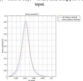
From our model, Figure 6 shows the potential distribution of the five-conductor transmission lines from (x,y) = (0,0) to (x,y) = (10,3) mm, using port 1 as input. Figure 7 shows the comparison analysis of potential distribution of the model with and without dielectric substrate. It observed that the peak value of electric potential is increased as the dielectric is placed in the substrate.
(x,y) = (0,0) to (x,y) = (10,3) mm, using port 1 as input.
Figure 7. Comparison analysis of potential distribution of the model with and without dielectric substrate.
The following electrical parameters, capacitance per unit length matrix (
C
in pF/m), inductance perunit length (
L
nH/m), and Characteristicimpedances (
Z
in
) are found as:
115.182
-45.004
-45.004 148.036
C
The inductance and capacitance per unit length of multiconductor transmission lines are related as follows:
1o o o
L
C
, (1)where,
L
Inductance matrix.
1o
C
the inverse matrix of the capacitance of the multiconductor transmission line when all dielectric constants are set equal to 1.o
permeability of free space or vacuum.o
permittivity of free space or vacuum.395.2
82.6
[ ]
82.6
284.2
L
The characteristic impedance and capacitance per unit length of multiconductor transmission lines are related as follows:
Z
L
C
(2)57.1118
j20.82691
[ ]
36.2129
39.0046
Z
The above results show the finite element method results for the electrical parameter of asymmetric coupled microstrips on two-layer substrates.
2.2 Modeling of Four-Line Symmetric Coupled Microstrips with a Two-Layer Substrates
In this section, we illustrate the modeling of the four-line symmetric coupled microstrips with two-layer substrates. We focus on the calculation of capacitance per unit length, the capacitance with homogenous dielectric layer, inductance, and the characteristic impedance. In Fig. 8, we show the cross-section of four-line symmetric coupled microstrips with two-layer substrates with the following parameters:
w
width of strips = 0.5 mms
distance between two strips = 0.5 mmt
thickness of the strips = 0.01mm1
h
height of the first layer from the ground = 0.335 mm2
h
height of the strips from the first layer = 0.3 mmFigure 8. Cross-section of four-line symmetric coupled microstrips with two-layer substrates.
For the modeling, the geometry was enclosed by a 30 X 3 mm shield. Figure 9 shows the finite element mesh. Table 2 shows the statistical properties of the mesh. Figure 10 shows the 2D surface potential distribution of the transmission lines. Counter and streamline plots were presented in Figures 11 and 12 respectively.
Table 2: Mesh statistics
Items Value
Number of degrees of freedom 61115 Total Number of mesh points 2829
Total Number of elements 5428 Triangular elements 5428
Quadrilateral 0
Boundary elements 550
Vertex elements 24
Figure 10. 2D surface potential distribution of four-line symmetric coupled microstrips with two-layer
substrates.
Figure 11. Contour plot of four-line symmetric coupled microstrips with two-layer substrates.
Figure 12. Streamline plot of four-line symmetric coupled microstrips with two-layer substrates.
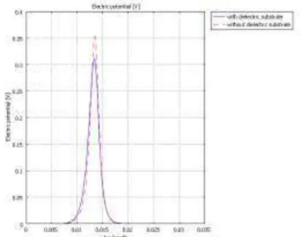
From our model, Figure 13 shows the potential distribution of the five-conductor transmission lines from (x,y) = (0,0) to (x,y) = (30,3) mm, using port 1 as input. Figure 14 shows the comparison analysis of potential distribution of the model with and without dielectric substrate. It observed that the peak value of electric potential is decreased as the dielectric is placed in the substrate.
Figure 13. Potential distribution of our-line symmetric coupled microstrips with two-layer substrates from (x,y) = (0,0) to (x,y) = (30,3)mm,
using port 1 as input.
Figure 14. Comparison analysis of potential distribution of the model with and without dielectric substrate.
The following electrical parameters (capacitance
per unit length matrix (
C
in pF/m), inductance perunit length (
L
in nH/m), and characteristicimpedances matrix (
Z
in
) are found as99.53343 29.54885 0.9212119 0.1340122
29.54885 109.6809 29.25836 0.9206155
0.9212119 29.25836 109.7019 29.56089
0.1340122 0.9206155 29.56089 99.53665
C
Using equation 1, we obtain
L
:440.1480 89.4267
26.0729
8.7115
89.2120
437.0070
88.7116
26.0747
[ ]
25.2873
88.5647
436.984334 89.4334
4.8237
25.2891
89.2186
440.1612
L
Using equation 1, we obtain
Z
:71.9285 49.9659 32.6158 20.8208
50.0898 73.1304 50.4437 32.7185
[ ]
32.5759 50.4054 73.1205 50.1127
19.6935 32.2822 49.8792 71.9106
Z
We provided the results of FEM in two-dimensional asymmetric coupled microstrips and four-line symmetric coupled microstrips with a two-layer substrates. The results of capacitance matrices for self and mutual capacitances, inductance matrix, and impedance matrices which are useful for the analysis of crosstalk between high-speed signal traces on the printed circuit board are obtained.
III.
Conclusions
In this paper we have presented the modeling of asymmetric coupled microstrips and four-line symmetric coupled microstrips with two-layer substrates using FEM. We have obtained the results for their electrical parameters such as the capacitance-per-unit length, inductance, impedances and we provided the potential distribution spectrums of the models and their meshing analysis.
References
[1.] C. Wei, R.F. Harrington, J.R. Mautz, and T.K. Sarkar, “Multiconductor transmission lines in multilayered dielectric media,” IEEE Trans Microwave Theory, vol. 32, pp. 439– 445, 1984.
[2.] R.F. Harrington and C. Wei, “Losses on multiconductor transmission lines in multilayered dielectric media,” IEEE Trans Microwave Theory Tech, vol. 32, pp. 705– 710, 1984.
[3.] W. Shu and S. Xu, “Capacitance extraction for multiconductor transmission lines in multilayered dielectric media using the numerical green’s function,” Microwave Opt. Technol Lett., vol. 40, pp. 529 –531, 2006.
[4.] G. Plaza, F. Mesa, and M. Horno, “Quick computation of [G], [L], [G], and matrices of multiconductor and multilayered transmission systems,” IEEE Trans Microwave Theory Tech., vol. 43, pp. 1623–1626, 1995.
[5.] W. Delbare and D. de Zutter, “Space -domain green’s function approach to the capacitance calculation of multiconductor lines in multilayered dielectrics with improved surface charge modeling,” IEEE Trans Microwave Theory Tech., vol. 37 , 1562–1568, 1989.
[6.] A. Papachristoforos, “Method of lines for analysis of planar conductors with finite thickness,” IEEE Proc Microwave Antennas Propag., vol. 141, 223–228, 1994.
[7.] L. Shujing and Z. Hanqing, “An efficient algorithm for the parameter extraction of multiconductor transmission lines in multilayer dielectric media,” Proc IEEE Antennas Propag Soc Int Symp A 3, pp. 228–231, 2005.
[8.] W. Delbare and D. de Zutter, “Accurate calculations of the capacitancematrix of a multiconductor transmission line in a multilayered dielectricmedium,” IEEE Microwave Symp Dig, Long Beach, CA , pp. 1013–1016, 1989.
[9.] J.J. Yang, G.E. Howard, and Y.L. Chow, “Complex image method for analyzing multiconductor transmission lines in multilayered dielectric media,” Int Symp Dig Antennas Propag, London, Ontario, Canada, pp. 862–865, 1991.
[10.] J. P. Gilb and C. A. Balanis, “Transient analysis of distortion and coupled in lossy coupled microstrips,” IEEE Transactions on Microwave Theory and Techniques, vol. 38, no. 12, Dec. 1990.