© 2007 Science Publications
Teaching Computer Organization and Architecture Using Simulation and FPGA
Applications
Dr. Kasim M. Al-Aubidy
Computer Engineering Department, Philadelphia University, P O Box 1, Jordan, 19392
Abstract: This paper presents the design concepts and realization of incorporating micro-operation simulation and FPGA implementation into a teaching tool for computer organization and architecture. This teaching tool helps computer engineering and computer science students to be familiarized practically with computer organization and architecture through the development of their own instruction set, computer programming and interfacing experiments. A two-pass assembler has been designed and implemented to write assembly programs in this teaching tool. In addition to the micro-operation simulation, the complete configuration can be run on Xilinx Spartan-3 FPGA board. Such implementation offers good code density, easy customization, easily developed software, small area, and high performance at low cost.
Key Words: Teaching tool, Computer organization and architecture, Processor design, Microprogramming, Assembler design, FPGA implementation.
INTRODUCTION
Computer organization and architecture is a common course that is offered at universities throughout the world [1]. Traditionally, teaching such a course to computer engineering and computer science students can be insufficient if the teaching focus is solely on textbook materials [2,3]. Students often have to rely on their imaginations to understand the underlying hardware-related concepts. In most universities, students learn computer design concepts by software implementing individual pieces of a computer. This approach has several limitations, while students can simulate their design using software, they don’t have the chance to realize or run their design in hardware [4]. Also, it is not feasible to build a laboratory that can provide various computer architectures for teaching computer organization and architecture. Hence, keeping computer education up-to-date requires keeping in touch with the rapid evolution of the computer technology and industry. Searching for an efficient way of teaching computer organization and architecture is an ongoing task [2]. An active tool will be considered in this paper for teaching computer organization and architecture by taking advantage of simulation and Field Programmable Gate Array (FPGA) technology [5,6]
.
FPGA technology offers the potential of designing high performance systems at low cost. FPGAs have been used for many computational tasks [6], and this paper presents the micro-operation simulation of a basic computer and its implementation on an FPGA. Field
programmable gate arrays consist of programmable logic blocks, which can each implement a small amount of digital logic, and programmable routing which allows the logic block inputs and outputs to be connected to form larger circuits [7,8,9].
FPGAs have become a popular technology for creating digital systems since they can lead to a shorter time-to-market for designs than application-specific circuits (ASICs) and allow design modifications to be made after system creation [10]. The primary method used for validating a design with most FPGA design flows is simulation.
This paper presents the micro-operation simulation and FPGA realization of a single cycle computer, which can be used for educational purposes. This simulation is a set of micro-operations that represent the register transfer statements of all operations that can be implemented. Also, it covers the design of an assembler for the designed computer, which can be used for educational purposes. The student can obtain a better understanding of the internal operation of a computer by simulating each element, and this will help students to study the design and performance issues.
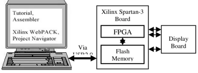
Fig. 1: Teaching Tool Layout
Xilinx Spartan-3 Board
FPGA
Flash Memory
Display Board Via
COMPUTER ORGANIZATION TEACHING TOOL
The design of the computer's instruction set is an important architectural issue. The processor structure and the functionality of the instructions define the computer's behavior. The objective of this work is to design a simple computer that will introduce the single-cycle computer features to the students. The internal organization of a digital system is defined by sequence of micro-operations that perform on data stored in its registers. The computer is capable of executing various micro-operations and can be instructed to perform a sequence of operations.
I1 I0 Op-Code Address/Data 15
Fig. 2: Instruction Format
Each component in the proposed computer was designed using Verilog HDL. Some components (e.g. Main Memory, Registers, …etc) have several modules in order to enable the user to choose his own architecture. To realize this choice a special GUI software was developed with multiple values selection for each component. These components include:
• Main Memory Size, which specifies the size of the
address field in the instruction format; and then the size of address related internal registers.
• Total number of instructions.
• Type of instructions; memory-reference (MRI),
register reference (RRI) and input/output reference (IOI) instructions, which results in determining number of cycles automatically.
• Computer Instructions; specify the required
instructions and their type to determine the size of the operation code in the instruction format and size of the op-code register automatically.
• Addressing Modes; which leads to determine the
number of required bits in the instruction format.
• Status Flags; specify the required flags such as
carry flag, zero flag and interrupt flag.
Once a student selects the design parameters, their values are written into a file used by the main module in the Verilog HDL code in order to build the required architecture. Then this architecture is downloaded into the FPGA using Project Navigator Package via USB port, see Fig.1.
DESIGN EXAMPLE
Instruction codes together with data are stored in memory. The computer reads each instruction from memory and places it in a control register. The control unit then interprets the binary code of the instruction and proceeds to execute it by issuing a sequence of micro-operations.
An instruction code is a group of bits that instruct the computer to perform a specific operation. It is made up of 16 bits, and divided into three parts, as shown in Fig.2. Two bits (I1,I0) to specify the addressing mode, four bits binary code to specify the operation, and ten bits address field. Table 1 illustrates the addressing mode of the proposed computer, which is used to:
• Reduce the number of bits in the address field of
the instruction, and
• Give user flexibility in dealing with counters,
pointers …etc
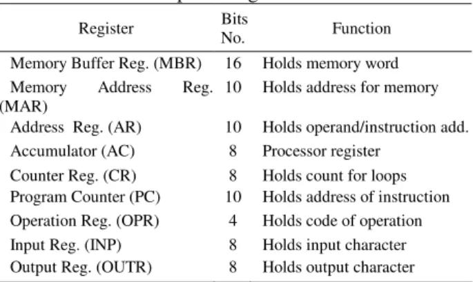
A computer needs registers for manipulating data and a register for holding a memory address. Nine registers are required for the proposed computer, as shown in Table 2.
Table 1: Addressing Modes.
Table 2: Basic Computer Registers.
Register Bits No. Function
Memory Buffer Reg. (MBR) 16 Holds memory word Memory Address Reg.
(MAR)
10 Holds address for memory
Address Reg. (AR) 10 Holds operand/instruction add. Accumulator (AC) 8 Processor register
Counter Reg. (CR) 8 Holds count for loops Program Counter (PC) 10 Holds address of instruction Operation Reg. (OPR) 4 Holds code of operation Input Reg. (INP) 8 Holds input character Output Reg. (OUTR) 8 Holds output character
Some registers (such as AC, MAR, and MBR) may receive data from several multiplexed sources. A basic computer has eight registers, a memory unit, and a control unit. Paths must be provided to transfer information from one register to another and between memory to registers. A more efficient scheme for transferring information in a system with many registers is to use a common bus. A multiplexer can be used to design the common bus. The connection of the registers to the common bus system is shown in Fig. 3.
Computer Instructions: A basic computer has three basic instruction code formats. A memory-reference instruction uses ten bits to specify either an address or an operand and two bits to specify the addressing mode (I0,I1). For immediate addressing it is 00, 01 for direct addressing, and 11 for indirect address. The register-reference instructions are recognized by the operation code 1111 and a 00 in the left most bits of the instruction. A register-reference instruction specifies an
I1 I0 Addressing mode
0 0 Immediate addressing ($ address) 0 1 Direct addressing
operation on the AC register. An operand from memory is not needed; therefore, the other 10 bits are used to specify the operation to be executed.
8 -to -1 M U X
M B R LD
O P R L D
IN P R LD
O U T R LD
b2 b1 b0
A R LD
P C LD
A C A L U
L D
1 6 -b it co m m o n b us
C LK C R LD
Fig. 3: Basic Computer Registers Connected to a Common Bus.
=1 R egister =1 Execute C ycle
Fetch C ycle
T1 Start T0 T1 T2 I1 =1 R egister or I/O =0 (Indirect or direct) I1
(D irect) =0 =1 (Indirect)
T0 T0 T1 T2 Execute input-output instruction Execute register-reference instruction Execute memory-reference instruction =1
(Interru pt C ycle) IN F
q1
I0
=0 (Im m ediate addressing)
=0 (I/O)
=0 (Fetch Cycle)
AR Address M BR
O PR, O P_C ode M BR ) I , (I I , I
M BR 0 1 0 1
> → < > → < > → <
M A R PC→
M B R
M (M AR)→
M AR
AR → AR →M AR
M BR M (M AR)→
AR Address M B R< > →
INF 0 , D ata M BR
P C→ < > →
M AR 0 PC,
0→ →
PC 1 PC M (M AR), D ata
M BR < > → + →
T0 T1 T2 PC 1 PC M B R,
M (M AR )→ + →
Fig. 4: Flowchart of Instruction Cycle
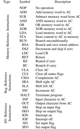
Table 3: Basic Computer Instructions. Type Symbol Description
NOP No operation
ADD Add memory word to AC SUB Subtract memory word from AC AND AND memory word to AC OR OR memory word to AC XOR XOR memory word to AC LDA Load memory word to AC STA Store content to AC in memory BUN Branch unconditionally
BSA Branch and save return address DSZ Decrement and skip if zero LDC Load CR
RET Return BZ Branch if zero
M em o ry R ef er en ce In st ru ct io n s
BC Branch if carry CLA Clear AC
CLS Clear all status flags CMA Complement AC
SRA Shift right AC SLA Shift left AC INC Increment AC
R eg . R ef er en ce In st ru ct io n s
HALT Terminate program INP Input character to AC OUT Output character from AC
SKI Skip on input flag SKO Skip on output flag ION Interrupt on IOF Interrupt off SFI Set input flag
I/ O R ef er en ce In st ru ct io n s
SFO Set output flag
Similarly, an input-output instruction does not need a reference to memory and is recognized by the operation code 1111 and 11 in the left most bits of the instruction. The remaining 10 bits are used to specify the type of the input-output operation. This technique allows having up to 35 different operations, as given in Table 3.
active timing signal to T0. The decoder is used to determine the cycle to be performed.
INSTRUCTION CYCLES
A program residing in the memory unit of the computer consists of a sequence of instructions. Each instruction cycle is subdivided into a sequence of sub-cycles. The value of three flip-flops is entered into a decoder to determine the cycle to be served, as illustrated in Table 4. As illustrated in Fig. 4, each instruction cycle is divided into the following five sub-cycles:
Fetch and Decode Cycle: Initially, the program counter is loaded with the address of the first instruction in the program. The sequence counter is cleared to 0, providing a decoded timing signal T0. After each clock pulse, sequence counter is incremented by one, so that the timing signals go through a sequence T0, T1, T2 and T3. The micro-operations for the fetch and decode cycle can be specified by the following statements: Cycle) (Indirect G 0 F, 0 R, 1 : T C I I Cycle) (Direct G 0 F, 1 R, O : T C I I Cycle) (Execute G 0 F, 1 R, 1 : T C I AR Address MBR OPR, OP_Code MBR ), I , (I I , I MBR : T C PC 1 PC MBR, M(MAR) : T C MAR PC : T C 3 0 0 1 3 0 0 I 3 0 0 1 0 1 0 2 0 1 0 0 0 → → → → → → → → → >→ < >→ < >→ < → + → →
Table 4:. Cycles Combination. Flip-flops
G F R Cycle
0 0 0 Fetch & Decode
0 0 1 Indirect
0 1 0 Direct
0 1 1 Execution
1 0 0 Interrupt
Indirect Cycle: At this cycle, the effective address of the operand is to be read from the memory. The register AR holds the address of memory word which contains the effective address of the operand:
Cycle) (Direct G 0 F, 1 R, 0 : T C AR Address MBR : T C MBR M(MAR) : T C MAR AR : T C 3 1 2 1 1 1 0 1 → → → >→ < → →
Direct Cycle: The effective address of the operand may be read during two time pulses. Therefore, to disable the delay of waiting for T3, the sequence counter may be cleared at time T2. Thus, the next time pulse will be T0 of the execution cycle and not T3 of the indirect cycle: Cycle) (Execution CC 0 G, 0 F, 1 R, 1 : T C MBR, M(MAR) : T C MAR AR : T C 2 2 1 2 0 2 → → → → → →
Execute Cycle: At this cycle, the fetched instruction (register-reference, memory reference, or input-output-reference) is executed. The type of the instruction is decided according to:
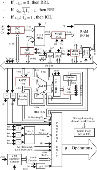
- If q15 =0, then RRI. - If q15I1I0 =1, then RRI. - If q15I1I0=1 , then IOI.
m PC 10-bit 2-to-1 MUX AR 10-bit MAR 10-bit RAM 1K*16 MBR 16-bit 16 Bits OPR 4-bit 4-to-16 Decoder C O N T R O L U N I T I1 I0 Operations − Status Flags (ZF & CF)
W
LD INC
LD
LD LD
LD LD INC 1 6 -b it 10-bit 10-bit 10-bit 10-bit 10-bit 10-bit 4-bit 4-bit 16-bit (q0-q15) S
Setting & resetting depend on ALU result
INP OUT 8-bit LD LD Clr ALU 4-bit
b2 b1 b0
8-bit
8-bit a1 a0
LD Inc Clr SR SL 4 -to -1 M U X AC 8-Bit Inverter 8-bit 8-bit MBR (0-7) 3-to- 8 Decoder 5-bit
(C0-C4)
R F G Set Rese Set Rese Set Rese INF 4-bit
(T0-T3)
2 -to -1 M U X 1 6 -b it 1 6 -b it
Set FGI (switch) Reset FGO (ACK)
ZF LD INC Clr CR LD Set Reset
CLK 2-bit
Sequence Counter
2-to-4 Decoder
CC
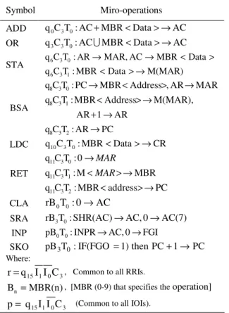
Table 5: Control functions and micro-operations for selected instructions
Symbol Miro-operations
ADD q0C3T0 :AC+MBR<Data>→AC OR q3C3T0 :AC MBR<Data>→AC
STA M(MAR) Data MBR : T C q Data MBR AC MAR, AR : T C q 1 3 6 0 3 6 → > < > < → → BSA PC AR : T C q AR 1 AR M(MAR), Address MBR : T C q MAR AR , Address MBR PC : T C q 2 3 8 1 3 8 0 3 8 → → + → > < → > < →
LDC q10C3T0 :MBR<Data>→CR
RET PC address MBR : T C q MBR M : T C q 0 : T C q 2 3 11 1 3 11 0 3 11 → > < → > < → MAR MAR
CLA rB0T0 :0→AC
SRA rB3T0:SHR(AC)→AC,0→AC(7) INP pB0T0:INPR→AC,0→FGI
SKO pB3T0:IF(FGO=1) then PC+1→PC Where:
3 0 1
15I I C
q
r = , Common to all RRIs. MBR(n)
Bn = , [MBR (0-9) that specifies the operation]
3 0 1
15I I C
q
p= (Common to all IOIs).
Interrupt Cycle: The interrupt cycle is initiated after the execute cycle if the interrupt flip-flop (INF) is equal to 1. The flip-flop is set to 1 manually using a switch, and it may be set during the execution of the program by the instruction ION. The flip-flop is reset to 0 whenever the interrupt is served or by the instruction IOF.
This basic computer serves the interrupt by saving the next sequential instruction in memory address 0, and then it starts execution from address 1 in the memory. The micro-operations required for this instruction are: Cycle) (Fetch G 0 F, 0 R, 0 : T C PC 1 PC M(MAR), Data MBR : T C MAR 0 PC, 0 : T C INF 0 , Data MBR PC : T C 3 4 2 4 1 4 0 4 → → → → + >→ < → → → > < →
Register Transfer Statements: A register transfer language is useful not only for describing the internal organization of the computer, but also for specifying the logic circuits needed for its design. The implemented computer has 35 instructions, as in Table 3. Each instruction is represented by a single statement or a set of statements. Table 5 illustrates the control functions
and micro-operations for selected instructions. The obtained statements give all the information necessary for the design of the logic circuits of the computer.
The schematic diagram of the basic computer is given in Fig. 5. It is compound of one 16-bit register, three 10-bit registers, four 8-bit registers, one 4-bit register, eight D-Flip-flops, one 1024x16-bit RAM, one ALU, one 8-bit inverter, two 2-to-1 Multiplexer, one 4-to-1 Multiplexer, one 4-4-to-16 decoder, one 3-to-8 decoder, one 2-to-4 decoder, and one 2-bit sequence counter.
ASSEMBLER DESIGN
A two pass assembler has been designed and implemented to write assembly programs and use the output of the assembler to run these programs on the basic computer. Figure 6 shows the files used as input and those generated as output by the assembler. These are;
• Source File (input): It is a text file containing the
source program to be assembled. It has a ".asm" extension. It consists of two segments, the code segment followed by the data segment. The data segment starts with "data:".
• Binary Code File (output): It contains the
assembled statements represented in binary form. This file is stored in the block memory, and it has a ".dat" extension.
• Hex Code File (output): It contains the assembled
statements in hexadecimal form. This file is stored in the external memory, and it has a ".mem" extension.
• Listing file (output): It consists of the source file
statements, the assembled code, and the Branch Vector Table BVT. This file has a ".lst" extension.
The basic computer assembly language character set consists of the following subset of the standard ASCII character set:
• Lower-case letters (a to z). • Digits 0 through 9. • Blanks (ASCII 32).
Assembler Instructions: Any assembly program for the basic computer consists of text lines, and each line contains only one instruction and an optional comment. Table 6 shows all instructions and their appropriate operands and addressing modes.
hex (.mem) and the binary (.dat) files. Comments may be added to lines that contain program code.
Fig. 6: Assembler Input and Output Files.
Table 6: Possible Types for Each Assembly Instructions
Instr. Type of operand Function
nop No operation
add Immediate data/Add.Add operand to AC sub Immediate data/Add.Subtract operand from AC and Immediate data/Add.AND operand to AC
or Immediate data/Add.OR operand to AC xor Immediate data/Add.XOR operand to AC lda Immediate data/Add.Load operand to AC
sta Address Store AC content in memory
bun Label Branch unconditionally
bsa Label Branch and save return add.
dsz Decrement and skip if zero
ldc Immediate data/Add.Load CR
ret Return
bz Label Branch if zero
bc Label Branch if carry
cla Clear AC
cls Clear all status flags
cma Complement AC
sra Immediate data Shift right AC
sla Immediate data Shift left AC
inc Increment AC
halt Terminate program
inp Input character to AC
out Output character from AC
ski Skip on input flag
sko Skip on output flag
ion Interrupt on
iof Interrupt off
sfi Set input flag
sfo Set output flag
Example: To write an assembly program for the implemented basic computer, follow these steps:
• Write an assembly program, using a text editor
such as Microsoft Notebook.
• Save the file as text only, using a ".asm" extension,
in the same directory as the Basic Computer Assembler.
• Using Windows Explorer or a command window,
start the assembler.
• When the assembler comes up, enter the name of
your file with .asm extension.
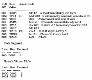
Fig. 7: Listing file of an assembly program.
Three new files are generated in the directory, the assembly language file with extensions .mem, and the list file with .lst extension (see Fig. 7), and the binary file have a "mem1.dat" name.
SIMULATION AND FPGA IMPLEMENTATION
Once files defining mico-operations are ready, the proposed computer can be entirely simulated with the simulator included in the Xilinx Development Environment. This is found particularly important to help students to;
• understand what is going on and why,
• check that obtained values from simulation confirm
to what is expected,
• verify and follow the progression of the signals
directly on the screen, since it matches the architecture layout given in Fig. 5.
Figure 8 shows the trace window for the signals generated by the assembly program given in Fig.7. By examining the control signals, contents of computer registers and memory at address 1 to 9 and at addresses 900, 901 1000 and 1001, we can determine whether the prototype is functioning correctly or not? Once we have Basic Computer Assembler
prog1.mem
Fig. 8: Waveforms Generated by the Program in Fig. 7.
Fig. 9: Teaching Tool Screen.
determined that the design is functioning correctly we are ready to proceed to the synthesis and device programming to generate a configuration that will program an FPGA device to implement the proposed computer system.
Field programmable gate arrays are a class of programmable logic devices based on an array of logic cells surrounded by a periphery of input/output cells. These programmable integrated circuits can be programmed in the field to implement specific design function. A basic computer architecture is created from the ground up as a scalable architecture, covering the basic operations in 16-bit processor domain.
The general layout of the user I/O user interface of the teaching tool is given in Fig. 9. An I/O interface is connected to the FPGA board to input any command or data from the student and to monitor current values of all registers, flags and related memory locations.
There are eight slide switches (SW0-SW7) in the
system. Switches (SW4-7) are used as input data,
Table 7: Device Characteristics
Device: Xilinx Spartan-3 XC3S200FT256 Slices: 3584, 256-ball thin Ball Grid Array System
gates
Logic cells Multipliers blocks (18*18)
Digital Clock Managers
Max I/O Signals
200 k 4320 12 4 173
Select RAM 18K-bits
Blocks
Max RAM K-bits
In-system programmable
configuration PROM
Fast Asynchronous SRAM
12 216 2 M-bits 1 M-byte
Table 8: Macro Statistics
ROMs 16x7-bit
Registers 17
Counters 3
Multiplexers 7
Tri-states 27
Decoders 2
Adders/Subtractors 4
Verilog Description Simple Computer
Design Specifications
Simulation
Error?
Yes Assembler Design
Specifications
Assembler Implementation
Emulation
Top Level Circuit Entry
Sub-Circuit Entry
Preliminary Choices of Leaf Parts
Error? Yes
Timing Constraints No
Error?
Synthesize No
Error? Yes
Place & Route
Error? No
Yes Run
Memory No
Machine Code
No
FPGA
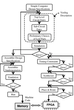
Fig. 10: Design Flow Map
Table 9: Utilization Summary
Item Used Available Percentage
Slices 433 3584 12%
Slice Flip Flops 114 7168 1%
4 input LUTs 802 7168 11%
Bonded IOBs 23 173 13%
GCLKs 2 8 25%
interrupts, while switch (SW0) is used to indicate if
the clock is a system clock or a user clock. Figure 10 shows the design procedure of the basic computer. Table 7 shows the different characteristics of the FPGA board used in the implementation[11,12. Tables 8 and 9 show the macro statistics and FPGA resources are shown in Tables 8 and 9 respectively.
CONCLUSION
This paper addressed the importance of using computer simulation and FPGA realization in learning computer organization and architecture. The given teaching tool can be considered as a useful practical addition to computer engineering and computer science curricula. This teaching tool helps computer engineering and computer science students to be familiarized practically with computer organization and architecture through development of their own instruction set and computer programming and interfacing experiments. In this paper;
• The simulation of a single cycle basic computer
and the implementation of an assembler has been presented.
• The micro-operation of the computer module and
its assembler are implemented on Xilinx Spartan-3 FPGA board, since it offers good code density, easy customization, easily developed software, high performance and small area.
• It is worthwhile to mention that this teaching tool
has been developed and implemented using popular Xilinx boards found in many universities. It has been tested by 3rd year undergraduate students enrolled at the computer architecture course given at Philadelphia university-Jordan. The students performed better when they used this teaching tool.
• The codes of the various modules are
implemented and tested with a program which utilizes every instruction as well as exercises the critical paths of the chip.
• This FPGA application runs at a maximum
REFERENCES
1. Holland, M., J. Harris and S. Hauck, 2003. Harnessing FPGAs for computer architecture education, Proceedings of the IEEE Intr. Conf. on Microelectronic Systems Education (MSE03), USA.
2. Hatfield, B. and M. Rieker, 2005. Incorporating simulation and implementation into teaching computer organization and architecture", 35th ASEE/IEEE Frontiers in Education Conf, Indianapolis, USA, pp: FIG-18.
3. Al-Aubidy, K. M., R. F. Al-Bader and A. A.
Samadi, 2005. Simulation and FPGA
implementation of a simple computer. The 7th Middle Eastern Simulation Multiconference "MESM2005", Porto, pp:151-158.
4. Quintans, C. and M. D. Valdes, L. Fernandez-Ferreira, M. J. Moure & E. Mandado, 2005. Digital electronics learning system based on FPGA applications, 35th ASEE/IEEE Frontiers in Education Conf, Indianapolis, USA, pp: S2G-7. 5. Li, Y. and W. Chu, 1996. Using FPGA for
computer architecture/organization education, EEE Computer Society Press, USA, pp.31-35.
6. Sugawara, Y. and K. Hiraki, 2006. A computer architecture education curriculum through the design and implementation of original processors using FPGAs, 36th ASEE/IEEE Frontiers in Education Conference.
7. Hennessy, J. L. and D. A. Patterson, 2003. Computer architecture: a quantitative approach, Morgan Kaufmann, USA.
8. Ciletti M. D., 2002. Advanced digital design with the Verilog HDL, Prentice Hall, USA. 9. Yalamanchili S., 2001. Introductory VHDL:
from simulation to synthesis, Prentice Hall, USA.
10. Krid M. and D. S. M. Masmoudi, 2005. FPGA implementation of a feedforward neural network, 3rd Intr. Conf. on Systems, Signals & Devices (SSD05), Tunisia, pp: .
11. Digilentic Co, 2004. Spartan-3 starter kit board
user guide, Digilentic Co.,
www.digilentinc.com.
12. ST Microelectronics, 2004. Design guide for