Tiago Jorge dos Santos Gameiro
Licenciado em Ciências da Engenharia de Micro e Nanotecnologias
RFID logic circuit with oxide TFTs modeled by
genetic algorithms
Dissertação para obtenção do Grau de Mestre em
Engenharia de Microeletrónica e Nanotecnologias
Orientador: Doutor Pedro Miguel Cândido Barquinha, Professor auxiliar, Faculdade de Ciências e Tecnologia da Universidade Nova de Lisboa Co-orientador: Doutor João Carlos da Palma Goes,
Professor Associado com Agregação, Faculdade de Ciências e Tecnologia da Universidade Nova de Lisboa
Júri
Presidente: Doutor Rodrigo Ferrão de Paiva Martins
Arguente: Doutor Jorge Manuel dos Santos Ribeiro Fernandes Vogal: Doutor Pedro Miguel Cândido Barquinha
RFID logic circuit with oxide TFTs modeled by genetic algorithms
Copyright © Tiago Jorge dos Santos Gameiro, Faculdade de Ciências e Tecnologia, Uni-versidade NOVA de Lisboa.
A Faculdade de Ciências e Tecnologia e a Universidade NOVA de Lisboa têm o direito, perpétuo e sem limites geográficos, de arquivar e publicar esta dissertação através de exemplares impressos reproduzidos em papel ou de forma digital, ou por qualquer outro meio conhecido ou que venha a ser inventado, e de a divulgar através de repositórios científicos e de admitir a sua cópia e distribuição com objetivos educacionais ou de inves-tigação, não comerciais, desde que seja dado crédito ao autor e editor.
Acknowledgements
This work culminates in the zenith of my education, the master’s degree in Micro and Nanotechnologies. Which would be impossible without the contribution of certain peo-ple.
First of all, I would like to thank Professor Rodrigo Martins and Professor Elvira Fortunato, for the creation of the course of Engineering in Micro and Nanotechnologies and also, for the opportunity to study and work in my thesis in CENIMAT|I3N and CEMOP as excellent investigation centers.
In second place, I would like to thank my adviser and co-adviser, Professor Pedro Barquinha and Professor João Goes for all the availability for my questions about my work and for all advices that helped enrich this master thesis. I would like to also thank to Professor Rui Tavares for all the help regarding genetic algorithms.
Also, would like to thank all people in CENIMAT and CEMOP that helped me inte-grate into this new environment, either by helping me at work or by all those afternoons playing football to clear our minds from everything else.
To all my friends and colleagues that helped me though this academic journey, and helped me study but also have fun. First of all, to my two friends, Shiv Bhudia and João Coroa, for all the hours, studying, playing games and partying, it would not be the same without you. Also, to my main man Nuno Pinela for all the support and help in these final years of the course. Finally, to my south margin bro, Viorel Dubceac, for all the hours discussing electronics, technology and life in general.
Also, I would like to thank my friends that helped me during the 6 months of thesis, mainly Cátia and Inês for your patience in putting up with me and distracting me from doing a better job in my master thesis. To my VFX friend, Marco Moreira for all the help studying and to understanding the university world. To all people from Serrado and surroundings, Chico, Jolu, David, Alex, Xana, Pires, Oliveira and Samouco. Finally, to all people that I forgot to mention here, but know that are my friends.
To my friends from Pombal, André, Henrique and Bernardo, for all the good times and especially for all those hours bowling and jamming.
In conclusion, to my family, without them I could not be here. Thanks for all the help and the opportunity to have an education for the future. To my mother, my father, my sister and my godfathers, Rosa e Daniel. Thank you all.
Abstract
In recent years, the need for identification techniques, with faster reading speed and more flexibility regarding memory and programmability, led to the development of Radio Frequency Identification technologies. This technology has already proven to be essential in the future of Internet-of-Things, by allowing the possibility of tagging any type of product easily and at low cost per tag, while also allowing the interface of these tags, with common smartphones to increase the connectivity of RFID devices in daily life. Furthermore, the introduction of amorphous IGZO thin film transistors in RFID circuits, opens a new world of applications since this type of devices allows the use of transparent and/or flexible substrates, due to the low temperatures required during the fabrication process.
In this work, it was used the a-Si Level 61 TFT Model together with genetic algorithms, to model a-IGZO transistors produced, with a gate dielectric deposited by a solution method using spin coating. With these models, it was designed an RFID logic circuit, which employs diode connected structures, to read a 16-bit Read Only Memory and encode the signal using a Manchester encoding technique, with a data rate of 14 kbit/s.
These types of circuits using transparent and/or flexible substrates could allow, in the future, the creation of smart packaging for regular house goods and integrate it in a smart fridge configuration. Meaning that, it could be possible to a person either to be advised when to buy a certain item or when it reaches the expiration date.
Keywords: a-IGZO, RFID, Thin Film Transistor, Genetic Algorithm, IoT.
Resumo
Nos últimos anos, a necessidade por técnicas de identificação com velocidades de leitura superiores e maior flexibilidade relativamente à memória e programabilidade, levaram ao desenvolvimento de tecnologias de identificação de rádio frequência (RFID). Esta tecnolo-gia já provou o seu valor no futuro da Internet das coisas (IoT), ao permitir a possibilidade de marcar qualquer tipo de produto facilmente e com baixo custo por etiqueta, enquanto possibilita a conexão deste tipo de etiquetas com smartphonespara aumentar a ligação entre os dispositivos RFID e a vida quotidiana. Além disto, a introdução de transísto-res de filme fino (TFT) de óxidos amorfos em circuitos RFID, abre um novo mundo de aplicações, visto que este tipo de dispositivos permite o uso de substratos transparentes e/ou flexíveis, devido à possibilidade de usar baixas temperaturas durante o processo de fabrico para este tipo de transístores.
Neste trabalho, foi usado o Modelo a-Si Nível 61 com a ajuda de algoritmos genéticos para criar modelos de transístores de a-IGZO produzidos com um dielétrico de porta depositado por métodos de solução usandospin-coating. Com estes modelos, foi dimensi-onado um circuito digital de RFID, usando uma topologia em que o transístor de carga está em configuração de díodo, para ler uma memória ROM de 16-bit e posteriormente codificar o sinal através de uma codificação deManchestercom uma taxa de transferência de 14 kbit/s.
Este tipo de circuitos utilizando substratos transparentes e/ou flexíveis pode possibi-litar no futuro a criação de embalagens inteligentes para bens domésticos e a posterior integração numa configuração de frigoríficos inteligentes. Isto significa que poderá ser possível uma pessoa ser avisada quando é necessário comprar um produto ou quando ultrapassa o prazo de validade.
Palavras-chave: a-IGZO, RFID, Transístores de Filme Fino, Algoritmos Genéticos, IoT.
Contents
List of Figures xv
List of Tables xvii
Acronyms xix
Motivation and Objectives xxi
1 Introduction 1
1.1 RFID Principles . . . 1
1.1.1 Types of RFID . . . 1
1.1.2 Operation and Parts of RFID devices . . . 1
1.2 Thin Film Transistors in RFID tags . . . 2
1.3 State of the Art . . . 3
1.3.1 TFT Modelling. . . 3
1.3.2 RFID Circuit . . . 4
1.4 Outline . . . 5
2 TFT Modelling 7 2.1 Level 61 a-Si TFT Model . . . 7
2.2 Parameter Extraction . . . 8
2.2.1 Genetic Algorithm . . . 8
2.2.2 DC Component . . . 10
2.2.3 AC Component . . . 11
2.3 Final Model . . . 12
3 Circuit Simulation 13 3.1 Basic Logic Circuits . . . 13
3.2 Exclusive Or . . . 14
3.3 Flip-Flop . . . 14
3.4 Clock generator . . . 15
3.5 5-bit Counter. . . 16
3.6 4 Line Select . . . 17
3.7 4 to 1 Multiplexer . . . 18
3.8 16-bit Read Only Memory . . . 18
3.9 Manchester Encoder. . . 18
3.10 Final Circuit . . . 20
3.11 Auxiliary Testing circuitry . . . 21
3.11.1 ESD protection circuit . . . 21
3.11.2 Output Buffer . . . . 22
CO N T E N T S
4 Layout and Test setup 25
4.1 Layout Description . . . 25
4.1.1 Fabrication Considerations. . . 25
4.1.2 Proposed Layout . . . 26
4.2 Test Setup . . . 27
5 Conclusions and future perspectives 29 Bibliography 33 A State-of-the-art 37 B Model Equations 39 B.1 Temperature Dependence . . . 39
B.2 Drain Current . . . 39
C Model Parameters 41
D Truth Tables 43
E Complete Layout 45
List of Figures
1.1 Representation of an RFID system. . . 1
1.2 (a) RFID parts; (b) RFID tag. . . 2
2.1 Variation of the total sheet density regarding the gate-source voltage. . . 8
2.2 Diagram of a genetic algorithm. . . 9
2.3 Cross-section of the TFTs modeled. . . 10
2.4 Capacitance as a function of gate voltage. . . 11
2.5 Comparison between Experimental curves and Model curves. . . 12
3.1 Block diagram of the RFID logic circuit. . . 13
3.2 Basic logic gates. . . 13
3.3 Exclusive Or gate. . . 14
3.4 Inputs and Outputs of the D-Type Flip-Flop.. . . 14
3.5 D-Type Flip-Flop. . . 15
3.6 Schematic of the clock generator. . . 15
3.7 RO frequency per stage capacitance. . . 16
3.8 Schematic of the 5-bit Counter. . . 16
3.9 Logic behavior of a 1-bit Counter. . . 16
3.10 (a) Schematic of the 4 Line Select circuit; (b) Schematic of the 4 to 1 Multiplexer. 17 3.11 Experimental simulation of the 5 bit-Counter and 4 Line Select. . . 17
3.12 Inputs and output of the 4 to 1 Multiplexer. . . 18
3.13 (a) Schematic of the ROM; (b) Circuit of the Manchester encoder. . . 19
3.14 Experimental simulation of the XOR gates of the encoder. . . 19
3.15 Enable, inputs and output of the DFF employed in the Manchester encoder.. 20
3.16 Experimental simulation of the ROM and the complete RFID circuit.. . . 21
3.17 ESD protection circuit. . . 21
3.18 Schematic of the output buffer driver.. . . . 22
3.19 (a) High gain inverter; (b) Comparison between regular and high gain inverter. 22 3.20 RFID logic circuit output with and without a buffer stage. . . . . 23
4.1 Cross section of a transistor and a via with passivation layers. . . 25
4.2 Proposed layout for the RFID digital circuit. . . 26
E.1 Complete layout of the RFID logic circuit. . . 45
List of Tables
2.1 Sweep values of each curve measured. . . 10
2.2 Dimensions and overlap capacitances of each transistor modeled. . . 12
3.1 Dimensions of the transistors presented in Figure 3.2. . . 14
3.2 Dimensions of the two high gain inverters employed in the output buffer . . 23
5.1 Average error of the model.. . . 29
5.2 Features of the RFID logic circuit. . . 30
A.1 Summary and comparison of State-of-the-art. . . 37
C.1 List of the parameters for the Level 61 a-Si TFT Model.. . . 41
D.1 Truth table of the exclusive OR. . . 43
D.2 Truth table of the D-Type Flip-Flop. . . 43
D.3 Truth table of the 4 Line Select circuit. . . 43
D.4 Truth table of the 4 to 1 multiplexer. . . 44
Acronyms
ANN Artificial Neural Network.
AOS Amorphous Oxide Semiconductor.
CMOS complementary Metal Oxide Semiconductor. CV Capacitance-Voltage.
DFF D-Type Flip Flop.
GA Genetic Algorithm.
GPS Global Positioning System.
HDL Hardware Description Language.
IGZO Indium Gallium Zinc Oxide. IoE Internet-of-Everything. IoT Internet-of-Things.
MOSFET Metal Oxide Semiconductor Field-Effect Transistor.
MUX Multiplexer.
NFC Near Field Communication. NRZ Non Return to Zero.
RF Radio Frequency.
RFID Radio Frequency Identification. RO Ring Oscillator.
ROM Read Only Memory.
SPICE Simulation Program with Integrated Circuit Emphasis.
TFT Thin Film Transistor.
VLSI Very Large Scale Integration.
Motivation and Objectives
In recent years, the technological development of industry and the growing population of the world, increased the logistical complexity of, for example, the distribution of goods around the world. This demanded new challenges, mainly in identification technologies. For many years, the barcode has been used due to its simplicity and extremely low cost. However, this technology has low storage capacity and requires a line of sight between the label and the reader besides, the barcode cannot be reprogrammed. The logical solution is the use of identification technologies with integrated circuits, like smart cards, which are nowadays the most common form of electronic data-carrying device [1]. However, in harsh factory environments, due to the impracticality of the contact reading systems and its speed, the smart card is not the best choice.
The optimal solution is a contactless system that would allow fast reading speed while maintaining low cost per tag. It would also be interesting that each tag could harvest the required energy from the reader [1]. All this is possible withRadio Frequency Identifica-tion (RFID)systems, which, as the name would suggest, relies onRadio Frequency (RF)
waves to send the identification signal to the reader [2].
Apart from the use of RFID devices in the control of products through factories, these systems are also used in contactless smart cards as tickets for short distance public transports, employee schedule control in work stations, inventory check and in anti-theft systems of retail establishments, for example in clothing stores.
The possibility of introducing amorphous oxide semiconductorThin Film Transistors (TFTs)in the manufacturing process ofRFIDelectronic circuits could lead to a new world of possibilities for low costRFIDdevices. This type of transistors can be fabricated with low temperature processes meaning they can be used in transparent/flexible substrates. This also means that the fabrication process can be easily reproduced in foundries not standardized with regular fabrication models. Hence, it is required to model transistors before starting the design and simulation of any circuit.
With this in mind, the objective of this work is to determine the parameters of amor-phousIndium Gallium Zinc Oxide (IGZO) TFTsfor the Level 61 a-SiTFTModel using
Genetic Algorithms (GAs). Then, these models will be used to designed a digital circuit for an RFID tag. At CENIMAT/CEMOP in FCT/UNL, the fabrication of bottom gate n-type a-IGZO transistors is optimized, so the diode-connected load will be the topology used in this circuit.
C h a p t e r
1
Introduction
1.1 RFID Principles
1.1.1 Types of RFID
Recently, the identification market has grown exponentially, and in the vanguard of this market, there are theRFIDdevices, which are capable of transmitting their identification code at high data rates and without line of sight between reader and tag, unlike previous identification techniques.
It is possible to divideRFIDdevices into two types: active and passive. The former one has a built-in power source, which means that this type ofRFIDhas a limited lifetime. This type of tags can be found in devices used to locate stolen cars incorporated with
Global Positioning System (GPS) and cellular technology [3]. Since there is a higher power budget, it is possible to include more power demanding circuits. On the other hand, passiveRFIDtags harvest the required energy from the carrier wave of the reader. This allows the tag to function indefinitely and reduce the overall cost. Nowadays, passive tags are more common in RF identification due to the advantages stated before, when compared to active tags and this will be the only type of tags mention throughout this work.
1.1.2 Operation and Parts of RFID devices
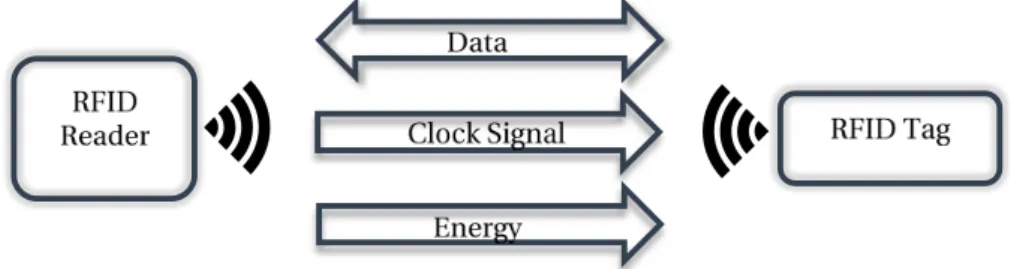
A common passiveRFIDdevice consists of a reader talk first protocol [1], meaning that the reading process starts with theRFIDreader sending a signal to the tag or transponder. This signal is then rectified to produce the DC signal required for the circuit to work, also in some cases, the signal sent from the reader is used as the clock signal for the circuit. After the rectification process, the integrated circuit sends the data back to the reader which can be, depending on the application, a serial code, a batch number or a production date. In Figure1.1it is shown a simplified representation of everyRFIDsystem.
Figure 1.1: Representation of an RFID system.
C H A P T E R 1 . I N T R O D U C T I O N
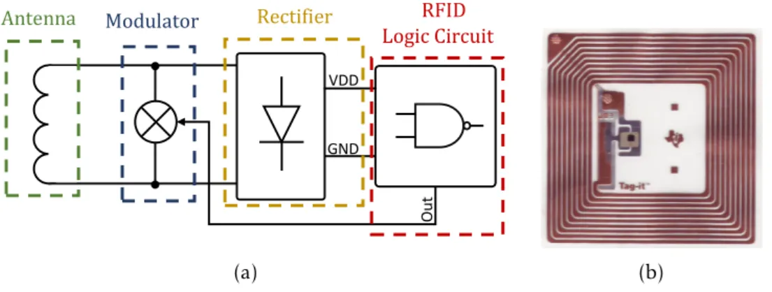
The parts that make a commonRFIDtag are as follows:
• An antenna, which consists of a coil and is used to receive and send signals to and from the reader;
• A modulator, used to up-convert the digital signal to the carrier to be sent to the antenna;
• A rectifier, used to down-convert the carrier signal into a DC signal.
• A logic circuit, responsible to generate the data, either by reading a memory or by using decoders to produce the desired bit sequence.
In Figure1.2are represented the main blocks of anRFIDtag and a commonRFIDtag, notice the coil as the antenna and the black square as the integrated circuit.
VDD
GND
Out
Antenna Modulator Rectifier RFID
Logic Circuit
(a) (b)
Figure 1.2: (a) RFID parts; (b) RFID tag.
1.2 Thin Film Transistors in RFID tags
For years,RFIDtags have been made using conventional siliconVery Large Scale Integra-tion (VLSI)technology, however this also meant that due to the configuration of regular
Metal Oxide Semiconductor Field-Effect Transistors (MOSFETs)it was impossible to use
these circuits in flexible and/or transparent substrates, since these types of transistors require a substrate contact (bulk) and high temperature fabrication processes. However, withTFTs, this is no longer the case, since these types of devices use only the substrate as a support for the transistor structure [4]. At the same time, all the layers that make the
TFTsare deposited through low temperature techniques (typical between room tempera-ture and 350◦C, depending on the TFT technology), unlike in silicon fabrication methods where it is required, for example, oxidation and recrystallization steps which need very high temperatures (up to 1000◦C).
Despite the lower fabrication temperatures, and hence the lower cost of the overall production price, TFTs have lower performance when compared with regular silicon
1 . 3 . S TAT E O F T H E A R T
MOSFETs. However, it was already shown that of all types ofTFTs,Amorphous Oxide Semiconductors (AOSs) show relatively high mobility, (from 1 to 100 cm2V−1s−1 [4]) when compared to other types ofTFTs, while maintaining low cost and low processing temperature. In this work the dimensions of the transistors used are very low to make up the low mobility when compared to silicon devices. The main problem withAOSsis the maturity of the technology which results in low yield and limited industrial application, unlike a-Si:HTFTswhich have been studied for almost forty years and are used in switch-ing elements in liquid crystal displays. [5]. However, regarding environmental concerns, oxideTFTsare eco-friendlier then a-Si:HTFTs, since the physical techniques employed use only Argon and Oxygen, unlike explosive gases as silane, phosphine or diborane [5]. The use of this different type of transistors allows for slightly different applications
than the originalRFIDdevices. Instead of a more industrialized use,RFIDtags with Ox-ideTFTsallow for the development of tags inserted in applications closer to the consumer. For example, usingRFIDdevices in flexible and/or transparent substrates for the creation of smart packaging labels, which can then be connected to theInternet-of-Things (IoT). This could allow the control, for example, of goods in a regular house fridge, giving infor-mation about the expiration date and the amount available of each product tagged. This technology can then be connect to theInternet-of-Everything (IoE)through smartphones withNear Field Communication (NFC)technology, allowing an even bigger integration ofRFIDdevices in daily life.
1.3 State of the Art
1.3.1 TFT Modelling
Before design and simulation of the desired circuit it is required a transistor model for the thin film transistors employed.
In modelling there are essentially two types of transistor models:
• Empirical models, where the behavior can be expressed using complex systems likeArtificial Neural Networks (ANNs)or mathematical expressions, in which, the parameters do not have physical meaning;
• Physical models, where the behavior is expressed using expressions which have parameters with physical meaning, like the threshold voltage;
1.3.1.1 Empirical Models
Regarding empirical models, it was shown in [6] how neural networks can be used to create models for amorphousIGZO TFTs and hence simulate with these models to de-sign circuits. Essentially,ANNsare an interconnection of a set of artificial neurons that have processing ability, and can learn to perform nonlinear modelling, with the help of experimental data, like output and capacitance curves for different bias and dimensions.
C H A P T E R 1 . I N T R O D U C T I O N
ForANNmodels, it is defined an equivalent circuit for the transistor with the overlap capacitances and the transistor’s voltage dependent current source, and each of these elements is modeled with the artificial neural networks [7], ensuring that the model can express not only the static, but also the dynamic behavior of the transistor. After the learning process, the model can be implemented in aHardware Description Language (HDL) to be straight forwardly used in a Simulation Program with Integrated Circuit Emphasis (SPICE)software.
1.3.1.2 Physical Models
Unlike empirical models, this type of models uses physical parameters to express the physical properties of the transistor. The Level 61 a-SiTFTModel is mainly a physical model with empirical expressions for the leakage region and is the one adopted in this work. This model has a high number of parameters, which means that it can be used to create models for transistors with high accuracy. However, this also means that it is necessary to extract a high number of parameters. It has already been shown in [8–11] several ways of extracting physical parameters through experimental transfer and output curves. Nonetheless, these methods of extraction can be very time consuming and are very dependent on the interval chosen for the extraction. For example, to extract the threshold voltage, one can select a certain interval of values to do a linear fit. However, with a slightly different interval, the extracted value can differ enough to change the
behavior of the physical model. To overcome this issue, in this work it is proposed and used a genetic algorithm, which is discussed in more detail in Chapter2. Essentially, this algorithm is a complex fitting tool used to determine the physical model parameters using the experimental curves as a target data.
In [12] it was used a combination of a genetic algorithm and a neural network to create a model for a GaN high electron mobility transistor. For this model, the genetic algorithm has been used to extract the extrinsic elements of the equivalent circuit model, while the intrinsic part was modelled using the neural network. Other uses of genetic algorithms include optimization tools in circuit design as seen in [13,14].
1.3.2 RFID Circuit
Most papers published in this area employ similar circuits, read a memory or generate a bit array and posteriorly encode that array. However, they differ in the topology or
fabrication methods.
In [15], it is represented a full RFID chip, including the RF circuit and the logic circuit. The circuit proposed, uses amorphous IGZO TFTs with an “active” load logic, this means that it is possible to achieve very low power consumption, of about 20 µW at 5 V [15]. However this also means that the load transistors need to be depletion type transistors. In [15], the supply voltage is obtained through rectification of the carrier wave of the tag reader and the memory is 4-bitRead Only Memory (ROM)with a clock
1 . 4 . O U T L I N E
of 50 Hz. Since depletion type transistors require more masks than a circuit with only regular enhancement typeTFTs, it is more common to use the load transistor in a diode connection topology, meaning this transistor is always in the saturation active region.
In [16], it is presented a digitalRFIDblock using the diode connected topology. Un-like the previous paper, this circuit is not integrated with the rest of the blocks of the
RFID chip. However the supply voltage is meant to be obtained from the rectification of the reader signal. In [16], the memory is 16-bitROMwith a Manchester encoder that produces a 32-bit array which can then be sent to theRFcircuit at a rate of 3.2 kbit/s.
In [17], are presented 4 fullRFIDchips with antenna, rectifier and logic circuit. The logic circuit employed, produces a 12-bit array and it was design in 4 different topologies.
The first one consists in the use of a pseudo-complementary Metal Oxide Semiconductor (CMOS)topology as presented in [18], the second is the classical diode connected topology and the 2 other topologies consist in the use of transistors with 2 gates. The first topology has a regular gate and a 2ndgate on the level of the source-srain contacts, while the second topology has the 2ndgate on the level of the metalization lines above the transistors. In these last two topologies, the extra gate terminal is used to change the threshold voltage of the transistors to increase the robustness of the logic gates [17]. The 3-gate topologies and the pseudo-CMOS require an extra power supply and more transistors per gate. However they are more robust and have lower power consumption when compared to classic topologies.
Despite having high data rates, the previousRFIDchips were not in compliance of the standard protocols forNFC, however in [19] it is presented a fullRFIDchip with a 128--bitROMthat can be read with a smartphone or any averageNFCreader. The topology
employed in this paper is based in a pseudo-CMOS topology [18]. Also in this circuit, the clock signal is directly extracted from the carrier of the reader, this means that the circuit used in these blocks must be able to work at frequencies in the range of a few MHz. This was achieved through special implementations with a minimum channel length of 1.5 µm and with a top gate Self-Aligned fabrication method, which resulted in transistors with low overlap capacitance, allowing higher operating frequencies [19].
In AppendixA, it is presented the main features of the State-of-the-art.
1.4 Outline
This work is divided in five chapters, the first one is aboutTFTmodelling using the widely known Level 61 a-Si model and genetic algorithms to calculate the model parameters. In Chapter3, it is presented the circuit and the electric simulations. Then, in Chapter4, it is presented the proposed layout and test methodology. After that, the conclusions and future perspectives are drawn in Chapter5.
C h a p t e r
2
TFT Modelling
2.1 Level 61 a-Si TFT Model
To model the amorphousIGZO TFTdevices it was used the Level 61 a-SiTFTstandard Model. This model is the equivalent to the AIM-SPICE MOS15 model developed at Rens-selaer Polytechnic Institute [20] and is widely implemented in mostSPICE simulators, including Cadence 6. To express all working regions of the transistor this model has ex-pressions for all 3 regions of operation, here are represented some features of this model for each region:
• Above Threshold Region:
– Linear region: Uses the classical square lawIDS model of crystalline silicon,
however for amorphous silicon transistors, it is necessary to include the field effect mobility as a function of gate voltage [10], as seen in (B.11), (B.12) and
(B.17).
– Saturation region: Like in linear region the saturation region has the field effect mobility as a function of gate voltage, (B.17). Also, to ensure a smooth
and continuous transition between linear and saturation region, the saturation voltage is replaced by the effective voltage which is a function of the saturation
voltage and a smoothness parameter [10], as seen in (B.22).
• Subthreshold Region: In this region, the Fermi level is in deep localized states and its position depends on the density of deep states. So, in this model the sheet density of free charges can be modeled as a function of gate voltage and the density of states [10], as seen in (B.16).
• Leakage Region: For this region, this model employs an empirical model to describe the leakage current as function of gate and drain voltages as seen in (B.7).
Finally, to improve convergence in circuit simulation, it is used a universal approach to unify the different model regions. The total sheet density of free charge is dominated
by the above threshold expressions at gate voltages higher than the threshold voltages while at lower voltages the total sheet density of free charge is reduced to subthreshold expressions as seen in Figure2.1.
After this, the model calculates the channel conductance hence the drain-source cur-rent.
It is important to note that, although this model is mainly dedicated to amorphous silicon, it is used for the AOSs TFTsused in this work. As stated before, this model is
C H A P T E R 2 . T F T M O D E L L I N G
-1 -0.5 0 0.5 1 1.5 2
V
GS (V)
100 105 1010 1015 1020 1025
Total Sheet Density of Free Charge
(C/m
2 )
nsa nsb ns
Model dominated by below threshold expressions, nsb Model dominated by above
threshold expressions, n sa
Figure 2.1: Variation of the total sheet density regarding the gate-source voltage. In blue is represented nsa, which is the total sheet density of free charge in above-threshold
region. In orange is represented nsb, which is the total sheet density of free charge in
subthreshold region. Finally in yellow is represented ns, which is the unified sheet density for all regions.
widely available in most simulators, unlike recent proposed physical models forAOSs TFTs, [21,22].
2.2 Parameter Extraction
The model employed is a physical model, which means that its parameters have physical meaning. To determinate each parameter through experimental curves it would be neces-sary to do several fittings due to the high number of parameters. However, even after the determination of all parameters, the model could not express the real operation of the
TFT.
2.2.1 Genetic Algorithm
In order to overcome this issue, it was used a genetic algorithm, to optimize the parame-ters so there is a good fit, not only to the transfer characteristics, but also to the output ones.
AGAis a search algorithm that uses the mechanics of natural selection to optimize complex systems [14]. InGAs, each parameter of the model is a gene and the vector of parameters is called a chromosome. Like most optimization algorithms theGAs deter-mines the correct elements of the chromosome that creates the best fit to a certain data (target values). Normally theGA is integrated with a simulator to evaluate each set of parameters. For circuit and model simulation the simulator can be a SPICEsimulator.
2 . 2 . PA R A M E T E R E X T R AC T I O N
However, when the fitness function is known, the model expressions can be used directly in the algorithm environment. In Figure2.2it is represented a diagram with the steps of the optimization process of theGA.
Figure 2.2: Diagram of a genetic algorithm adapted from [23].
As seen in Figure2.2, after the creation of the first population the optimization pro-cess is started. With this first population, it is determined the average error between the experimental curves and the curves generated by the model with the first population. If, after a modification in the chromosome, the error increases when compared with the previous generation, the probability of this modification appear in future generations is decreased. However, when the error is reduced after a modification, the process is the opposite. This process is called selection and it is the main way for the creation of new generations. A new generation can also be generated by crossover, when parent chromo-somes generate a child and by mutation, when random chromochromo-somes are generated to
C H A P T E R 2 . T F T M O D E L L I N G
maintain genetic diversity. However, this probability should be set low, otherwise the optimization will turn into a random search.
The algorithm will keep running until one of two things happen: the error calculated in each generation is lower than the target value or the maximum number of generations is reached. With this process of survival of the fittest and a random component, theGA
can avoid local minimums, which results in a robust optimization.
As stated before, the algorithm compares curves generated by the model and exper-imental curves, this curves can be considered the DC component of the model. For the AC component of the model, the parameters are calculated manually, since its values are easier to extract and do not require any kind of curve fit.
2.2.2 DC Component
In Figure2.3, it is represented the cross-section of the transistors modeled.
L
Lov
Lov
Figure 2.3: Cross-section of the TFTs modeled.
All layers were deposited usingRFsputtering while the dielectric layer was deposited by solution using spin-coating as demostrated in [24]. The gate, source and drain elec-trodes are Molybdenum and have a thickness of about 17 nm, 70 nm and 70 nm respec-tively. The dielectric layer is aluminum oxide and has a thickness of about 20 nm. Fi-nally, the semiconductor layer is composed of amorphousIGZOwith a thickness of about 22 nm.
The experimental curves were obtained with Cascade M150 and Agilent 4155c Semi-conductor parameter analyzer. The modulation was made using transfer and output curves and in Table2.1it is represented the sweep values for each curve.
Table 2.1: Sweep values of each curve measured.
Transfer Curve Output Curve VGS -1:0.06:2 0:0.5:2
VDS 2 0:0.05:2
In AppendixC, it is represented all parameters for the Level 61 a-Si model.
2 . 2 . PA R A M E T E R E X T R AC T I O N
2.2.3 AC Component
The AC component of the Level 61 a-S1 TFT Model calculates de source and gate--drain capacitances, respectivelyCgsandCgd, using several parameters. These parameters
include the substrate and gate insulator relative dielectric constant and gate-source and gate-drain overlap capacitance per channel width [20], respectively,Cgsov andCgdov.
The substrate used was Corning eagle xg which has a relative dielectric constant of about 5.3 at room temperature [25]. The remaining AC parameters can be determined fromCapacitance-Voltage (CV)curves. In Figure2.4its represented a typicalCVcurve.
-2 -1 0 1 2 3
V
G (V)
1.6 1.8 2 2.2 2.4 2.6 2.8 3 3.2 C (pF) C
Channel = CTotal - COverlap
Total Capacitance
Overlap Capacitance
Figure 2.4: Capacitance of a transistor withW/L= 100/5, as a function of gate voltage.
To obtain these curves, the source and drain were grounded while at the gate it was applied an AC signal with a frequency of 100 kHz, with a DC bias which was then swept between -2 and 3 V. The measurements were made in Cascade EPS150 triax and Keysight b1500a. The experimental setup is calibrated to exclude the capacitances of the test probes and the cables, meaning that the value measured is only from the transistors.
As seen in Figure2.4, in the subthreshold region only the overlap capacitance between the gate electrode and the source and drain electrode is measured. In the above-threshold region is measured the total capacitance of the device. The channel capacitance is given by the difference between the total capacitance and the overlap capacitance. Bearing this
in mind, it is possible to calculate the value of the relative dielectric gate insulator, which is given by expression (2.1).
εr=
Cch×d
ε0×W×L
(2.1)
whereCchis the channel capacitance obtained from theCVcurve;dis the thickness of
the gate insulator;ε0is the vacuum permittivity andWandLare the transistor’s width
C H A P T E R 2 . T F T M O D E L L I N G
and length, respectively.
Assuming the device is symmetrical, the gate-source and gate-drain overlap capaci-tance per channel width is simply the overlap capacicapaci-tance divided by 2 and then divided by the width of the measured device.
2.3 Final Model
With all DC and AC parameters extracted, the process has been repeated for 3 transistors with different dimensions, to have a robust model. These dimensions and the overlap
capacitance per channel width for each transistor are represented in Table2.2.
Table 2.2: Dimensions and overlap capacitances of each transistor modeled.
W (µm) L (µm) Cgdov/Cgsov(F m−1)
5 2 7.75×10⁻⁸ 50 5 1.27×10⁻⁸ 100 5 8.08×10⁻⁹
During circuit simulation, it were used different models for different transistor
dimen-sions. Also, to increase the range of dimensions available to simulation, it has been used in several cases, transistors in parallel or in series to increase theWorLrespectively. This way the overall dimensions of the transistor don’t change but the model can still express the operation of the transistor with a small error.
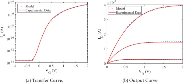
In Figure2.5a and Figure 2.5bare represented transfer and output curves, respec-tively of the experimental measurements and the model for the transistor withW/L =
50 µm/5 µm.
-1 -0.5 0 0.5 1 1.5 2
V G (V)
10-14 10-12 10-10 10-8 10-6 10-4 I D (A) Model Experimental Data
(a) Transfer Curve.
0 0.5 1 1.5 2
V D (V)
0 1 2 3 4 I D (A) 10-5 Model Experimental Data
(b) Output Curve.
Figure 2.5: Comparison between Experimental curves and the Model for the transistor withW/Lof 50/5.
C h a p t e r
3
Circuit Simulation
The transistors used in this work, a-IGZO TFTs, are n-type. Hence, it is employed a diode connected load topology, this means that all the basic blocks of the logic have a diode connected load to do the pull-up and several transistors, according to the respective gate, to do the pull-down. In Figure3.1, it is represented the block diagram that represents schematically theRFIDlogic circuit. Afterwards, each individual block is presented in more detail. In the end, it is also presented the auxiliary circuitry designed exclusively for testing purposes. Since the transistors used have a very thin dielectric, it is possible to use low supply voltages, in this case 2 V.
Out3 16-bit ROM 4 Lin e Select 4-1 Multiplexer 5-bit Binary Counter fc
fcΤ8
fcΤ16
fcΤ2
fcΤ4
fcΤ32
ROMOut Manchester Encoder Clock Generator Out2 Out1 Start RFIDOut Buffer ESD Protection Circuit
Figure 3.1: Block diagram of the RFID logic circuit.
3.1 Basic Logic Circuits
In Figure3.2, it is represented the NOT and NAND gate circuits used and, in Table3.1, it is presented the dimensions of each given device.
𝑉𝐷𝐷 𝑂𝑢𝑡 𝑀𝐿 𝑀𝐷 𝐼𝑛 𝐺𝑁 𝐷 𝑉𝐷𝐷 𝑂𝑢𝑡 𝑀𝐿 𝑀𝐷2 𝐺𝑁 𝐷 𝑀𝐷1 𝐼𝑛1 𝐼𝑛2 𝑉𝐷𝐷 𝑀𝐿 𝑀𝐷 𝐼𝑛 𝐺𝑁 𝐷 𝑉𝐷𝐷 𝑂𝑢𝑡 𝑀𝑂𝑢𝑡1 𝑀𝑂𝑢𝑡2 𝐺𝑁 𝐷
(a) NOT gate.
𝑉𝐷𝐷 𝑂𝑢𝑡 𝑀𝐿 𝑀𝐷 𝐼𝑛 𝐺𝑁 𝐷 𝑉𝐷𝐷 𝑂𝑢𝑡 𝑀𝐿 𝑀𝐷2 𝐺𝑁 𝐷 𝑀𝐷1 𝐼𝑛1 𝐼𝑛2 𝑉𝐷𝐷 𝑀𝐿 𝑀𝐷 𝐼𝑛 𝐺𝑁 𝐷 𝑉𝐷𝐷 𝑂𝑢𝑡 𝑀𝑂𝑢𝑡1 𝑀𝑂𝑢𝑡2 𝐺𝑁 𝐷
(b) NAND gate.
Figure 3.2: Basic logic gates, at transistor-level, used in this work.
C H A P T E R 3 . C I R C U I T S I M U L AT I O N
Table 3.1: Dimensions of the transistors presented in Figure3.2.
NOT NAND
Transistor ML MD ML MD1 MD2
W (µm) 10 50 5 50 50
L (µm) 2 2 2 2 2
3.2 Exclusive Or
The XOR gate, also known as exclusive OR, is a case of an OR gate, meaning that only when the inputs are different will the output be 1, as seen in TableD.1.
The schematic and symbol are represented in Figure3.3.
𝑉𝐷𝐷 𝑉𝑏𝑖𝑎𝑠
𝐶𝐿 𝑀𝐵 𝐷 𝐶𝐿𝐾 𝑄ത 𝑄 𝐼𝑛1 𝐼𝑛2 𝑂𝑢𝑡 𝐼𝑛1
𝐼𝑛2 𝑂𝑢𝑡
(a) Schematic.
𝑉𝐷𝐷 𝑉𝑏𝑖𝑎𝑠
𝐶𝐿 𝑀𝐵 𝐷 𝐶𝐿𝐾 𝑄ത 𝑄 𝐼𝑛1 𝐼𝑛2 𝑂𝑢𝑡 𝐼𝑛1
𝐼𝑛2 𝑂𝑢𝑡
(b) Symbol.
Figure 3.3: Exclusive Or gate.
3.3 Flip-Flop
The Flip-Flop used in this work is a positive edge-triggeredD-Type Flip Flop (DFF). This means that the output Q will be the input Data (D) when the clock signal is rising, as seen in TableD.2and Figure3.4.
0 1 2
Clock (V)
0 50 100 150 200 250
Time ( s)
0 1 2 Q (V) 0 1 2 Data (V)
Figure 3.4: Behavior of the Flip-Flop, showing that the output Q is Data when the clock signal is rising.
3 . 4 . C LO C K G E N E R ATO R
The flip-flop tested has a simulated rising time of 20 µs and a falling time of approxi-mately 9.4 µs. The circuit for the positive edge triggeredDFFis composed of NAND gates, and in Figure3.5it is represented its schematic and symbol.
𝐶𝐿𝐾
𝐷
𝑄ത 𝑄
(a) Schematic.
𝐷
𝐶𝐿𝐾
𝑄ത
𝑄
(b) Symbol.
Figure 3.5: D-Type Flip-Flop.
3.4 Clock generator
The clock generator is composed of a cascade 20 inverters and a NAND gate in a feedback loop, also known as aRing Oscillator (RO), Figure3.6. The first delay stage is a NAND gate to have the possibility to impose a variation in the circuit in case the circuit do not start in the test phase. For the RFIDlogic circuit it is required 3 signals with different
phases from each other, as seen in the block diagram of the circuit, represented in Fig-ure 3.1. The 3 outputs are as follows: Out1is node 3,Out2is node 9 andOut3is node
19 of theRO. It is also important to note that each output of the clock generator, prior to its application on the rest of the circuit, undergoes a buffering stage composed of a NOT
gate.
𝑆𝑡𝑎𝑟𝑡
𝑂𝑢𝑡1
തതതതതത 𝑂𝑢𝑡തതതതതതത3
𝐺𝑁𝐷 𝐺𝑁𝐷 𝐺𝑁𝐷 𝐺𝑁𝐷 𝐺𝑁𝐷
1 2 3 19 20 21
(…)
Figure 3.6: Schematic of the clock generator.
The frequency of theROdepends on the delay of each stage, so to decrease the oscilla-tion frequency it is added a capacitor between each inverter. In Figure3.7it is represented
C H A P T E R 3 . C I R C U I T S I M U L AT I O N
the variation of the frequency of theROas a function of the capacitance of the capacitor on each delay stage.
10-15 10-14 10-13 10-12 10-11 10-10 10-9
Capacitance (F) 0 10 20 30 40 50 Frequency (kHz)
Inverter with 21 delay stages: Capacitance per Stage: 10 pF Oscilation Frequency: 14 kHz
Figure 3.7: Variation of the RO oscillation frequency as a function of the stage capacitance.
For an oscillation frequency of 14 kHz the capacitor in each stage of theROmust have a capacitance value of 10 pF.
3.5 5-bit Counter
For the RFIDlogic circuit, it is required to divide the signal provided by the clock gen-erator 5 times, so using the DFFit was designed a 5-bit Counter, as seen in Figure3.8. Moreover, in Figure3.11ait is represented the input signal and the 5 output signals of the counter. 𝐷 𝐶𝐿𝐾 𝑄ത 𝑄 𝐷 𝐶𝐿𝐾 𝑄ത 𝑄 𝐷 𝐶𝐿𝐾 𝑄ത 𝑄 𝐷 𝐶𝐿𝐾 𝑄ത 𝑄 𝐷 𝐶𝐿𝐾 𝑄ത 𝑄
𝑓𝑐 𝑓𝑐 2Τ 𝑓𝑐 4Τ 𝑓𝑐 8Τ 𝑓𝑐 16Τ 𝑓𝑐 32Τ
Figure 3.8: Schematic of the 5-bit Counter.
In Figure 3.9it is represented the logic behavior of a 1-bit Counter (with only one Flip-Flop). The logic is repeated for a 5-bit Counter.
CLK
D
Q
Q
n0
1
0
1
1
0
1
0
0
0
1
0
1
1
0
1
0
1
0
1
Figure 3.9: Logic behavior of a 1-bit Counter.
3 . 6 . 4 L I N E S E L E C T
Since the Flip-Flop used is a positive edge-triggered, only when the signal is rising from 0 to 1 does the output Q is Data (green arrow in Figure 3.9). Assuming the first state of Q is 0, when the clock is enable (0 to 1 transition) the data value (1 due to the feedback) passes to the output Q and D goes to 0. After this, the clock goes from 1 to 0, but there is no change in the output, only after clock signal rises again does the output goes to 0. This means that at the output the signal change after two periods at the input.
3.6 4 Line Select
To select all lines of the memory it was designed the circuit represented in Figure3.10a, which generates a pulse that sweep all the outputs consecutively, allowing to activate one line of the memory at a time. This kind of circuit is also called a decoder and in TableD.3
it is represented the truth table of the circuit and in Figure3.11bit is represented the input and output signals of the 4 Line Select circuit.
𝑆0
𝑆1 𝐷0
𝐷1 𝐷2 𝐷3 (a) 𝑆0 𝑆1 𝐷0 𝐷1 𝑂𝑢𝑡 𝐷3 𝐷2 (b)
Figure 3.10: (a) Schematic of the 4 Line Select circuit; (b) Schematic of the 4 to 1 Multi-plexer. fc (V) fc/2 (V) fc/4 (V) fc/8 (V) fc/16 (V)
0 2 4 6 8 10
Time (ms) fc/32 (V)
(a)
S 0 (V)
S 1 (V)
D 0 (V)
D 1 (V)
D 2 (V)
1.2 1.4 1.6 1.8 2 2.2 Time (ms)
D 3 (V)
(b)
Figure 3.11: (a) Input and 5 outputs of the 5-bit Counter; (b) Inputs and outputs of the 4 Line Select circuit.
C H A P T E R 3 . C I R C U I T S I M U L AT I O N
3.7 4 to 1 Multiplexer
To read the columns of the memory it is used a 4 to 1Multiplexer (MUX), which takes the value of each column at a time and represents it in the output. The inputs of both the 4 line decoder and the multiplexer are the outputs of the 5-bit Counter (Figure3.1), meaning that for each cycle of the multiplexer only one line is activated at a time, the cycle is then repeated for the following line in memory.
In Figure3.10bis represented the circuit of the 4 to 1 MUXand, in TableD.4it is represented the truth table of the circuit. In Figure3.12it is represented the inputs and output of the Multiplexer for a test signal.
S 0 (V)
D 0 (V)
D 2 (V)
D 3 (V)
0 0.1 0.2 0.3 0.4 0.5 0.6 0.7 0.8
Time (ms)
Out (V) D 1 (V) S 1 (V)
Figure 3.12: Inputs and output of the 4 to 1 Multiplexer.
3.8 16-bit Read Only Memory
The memory employed is a 16-bitROMand its data is read by applyingVDDto the line of
the desired bit, this will turn on all transistors on that line. After this step, the voltage on each column is read sequentially, being 0 if a transistor is present and 1 if not, as described in Figure3.13a. The high value is obtained thanks to a diode connected transistor in each column.
3.9 Manchester Encoder
After theROMdata is read, the serial signal is encoded using a Manchester encoding Technique. The Manchester encoding is used in bit serial digital communications and is also known as phase encoding [2]. Unlike other type of encoding, this technique does
3 . 9 . M A N C H E S T E R E N CO D E R 𝐷0 𝑉𝐷𝐷 𝐺𝑁𝐷 𝐺𝑁𝐷 𝐺𝑁𝐷 𝐺𝑁𝐷 𝐷1 𝑉𝐷𝐷 𝐷2 𝑉𝐷𝐷 𝐺𝑁𝐷 𝐺𝑁𝐷 𝐺𝑁𝐷 𝐷3 𝑉𝐷𝐷 𝐺𝑁𝐷 𝐺𝑁𝐷 𝐿0 𝐿1 𝐿2 𝐿3 1 0 (a) 𝑀𝑈𝑋𝑂𝑢𝑡 𝑂𝑢𝑡2 𝑂𝑢𝑡1 𝑂𝑢𝑡3 𝐷 𝐶𝐿𝐾 𝑄ത 𝑄 𝑂𝑢𝑡 𝑂𝑢𝑡 തതതതത ME Data MEClock 1 2 𝐺𝑁𝐷
𝐸𝑛𝑏 𝑀1
(b)
Figure 3.13: (a) Circuit schematic of the implemented memory ROM employed. The data in the memory is 0101, 0100, 0100, 0111; (b) Circuit of the Manchester encoder.
not require the clock signal to be sent along with the serial signal, since Manchester encoding allows for easier synchronization with the receiver. Also, when compared to
Non Return to Zero (NRZ)encoding [2], Manchester encoding has less noise interference since this type of encoding has more level transitions which are easier to detect than constant signals in time. The circuit of the encoder is represented in Figure3.13band its input is the output of the Multiplexer as seen in Figure3.1.
This circuit was adapted from [16] and it is composed of 2 XOR gates and aDFF. The encoder is essentially one XOR gate, XOR 1, which the clock signal is one of the outputs of the ring oscillator, Out2. In Manchester encoding a 0 corresponds to a ’10’ transition
while the 1 corresponds to a ’01’ transition as defined by IEEE 802.3 standard [26]. The input and output wave forms of the XOR gate are represented in Figure3.14a.
0 1 2 MUX Out (V)
1.4 1.45 1.5 1.55 1.6 1.65
Time (ms) 0 1 2 ME Data (V) 0 1 2 Out 2 (V)
1 1 0
1 0
0 0
1
1 0 0 0
(a) Xor 1.
0 1 2 V (V) Out 1 Out3
100 150 200 250 300
Time ( s)
0.5 1 1.5
ME Clock V (V)
(b) Xor 2.
Figure 3.14: Inputs and Outputs of the two Exclusive OR gates of the Manchester Encoder represented in Figure3.13b.
C H A P T E R 3 . C I R C U I T S I M U L AT I O N
As seen in Figure3.14a, the output of the XOR gate produces a lot of undesirable volt-age peaks. Hence, to clean the output signal, it is used theDFFpreviously implemented. However, it is also required a clock signal with a higher frequency or since the DFFis positive edge-triggered, a clock signal with at least more signal transitions. For this, it is used a second XOR which the inputs are two more signals from the ring oscillator out of phase from each other, Out1and Out3, the result is shown in Figure3.14b.
0.5 1 1.5 2 Enable (V) 0 1 2 Data (V) 0.5 1 1.5 Clock (V)
1 1.5 2 2.5
Time (ms) 0 1 2 Output (V) Disable
Time Enable Time
Disable Time
Figure 3.15: Enable, inputs and output of the DFF employed in the Manchester encoder.
In Figure 3.13b, after the encoding process it is used a transistor, M1, to bring the signal to low state once the memory is read. The enabling signal is one of the outputs of the 5-bit Counter, with a frequency of fc/32, and for each period of this signal the memory is completely read, this allows the output signal to, periodically, show the desired signal as it can be seen in Figure3.15.
3.10 Final Circuit
In Figure3.16it is represented theROMsignal and the output signal of theRFID.
The power dissipation of theRFIDlogic circuit is determined by the expression (3.1):
PDD=IRMS×VDD (3.1)
whereIRMS represents the root-mean-square current consumption. With aVDD of 2 V the power dissipation of theRFIDlogic circuit is 810.8 µW. It is important to note that the output buffers have not been included in the determination of the power dissipation
3 . 1 1 . AU X I L I A RY T E S T I N G C I R C U I T RY 0 0.5 1 1.5 2 ROM Data (V)
1 1.5 2 2.5
Time (ms) 0 1 2 RFID Out (V)
10, 01, 10, 01, 10, 01, 10, 10, 10, 01, 10, 10, 10, 01, 01, 01 0 1 0 1, 0 1 0 0, 0 1 0 0, 0 1 1 1
Figure 3.16: ROM and output signal of the RFID after the Manchester encoding. In the Figure it is also represented the serial bit array of the ROM and the Manchester encoder.
3.11 Auxiliary Testing circuitry
3.11.1 ESD protection circuit
In Chapter2it was shown that the transistors used for this circuit have a dielectric with a thickness of about 20 nm, this means that the circuit is prone to dielectric breakdown in the face of an electrostatic discharge. This is even more critical for circuit inputs which are directly connected to gates of transistors, like the start pin represented in Figure3.6. To minimize this, it is used the circuit presented in Figure3.17a, consisting of two reverse--biased diodes and a resistor in order to limit the current flow and to drain excess current
to the rails. However, for the circuit to be fabricated in CEMOP at FCT/UNL, it is required to be made entirely ofTFT. In Figure3.17bit is represented the proposed circuit using TFT devices. 𝐺𝑁𝐷 𝑉𝐷𝐷 𝐼𝑛 𝑂𝑢𝑡 (a) Schematic. 𝐺𝑁𝐷 𝑉𝐷𝐷 𝐼𝑛 𝑂𝑢𝑡 𝑉𝐷𝐷 𝑀1 𝑀2 𝑀3
(b) TFT topology.
Figure 3.17: ESD protection circuit (primary protection only).
C H A P T E R 3 . C I R C U I T S I M U L AT I O N
3.11.2 Output Buffer
For testing purposes, it is necessary to design special buffers for properly driving the test
probes or, otherwise, the capacitive load of the probes colapses the signal, making very difficult to analyze the circuit. The circuit proposed consists of 2 inverters and 2 high
gain inverters cascaded in series, as presented in Figure3.18.
𝐼𝑛 NOT High Gain
NOT
NOT High Gain
NOT 𝑂𝑢𝑡
Figure 3.18: Schematic of the output buffer driver.
3.11.2.1 High Gain Inverter
The High Gain inverter has the same logic function as the inverter. However this circuit can drive a bigger load faster than a normal inverter and its circuit is represented in Figure3.19a.
𝑉𝐷𝐷 𝑂𝑢𝑡 𝑀𝐿 𝑀𝐷 𝐼𝑛 𝐺𝑁 𝐷 𝑉𝐷𝐷 𝑂𝑢𝑡 𝑀𝐿 𝑀𝐷2 𝐺𝑁 𝐷 𝑀𝐷1 𝐼𝑛1 𝐼𝑛2 𝑉𝐷𝐷 𝑀𝐿 𝑀𝐷 𝐼𝑛 𝐺𝑁 𝐷 𝑉𝐷𝐷 𝑂𝑢𝑡 𝑀𝑂𝑢𝑡1 𝑀𝑂𝑢𝑡2 𝐺𝑁 𝐷 (a)
0 50 100 150 200 250
Time ( s)
0 0.5 1 1.5 2 V (V)
Normal Inverter High Gain Inverter Input
(b)
Figure 3.19: (a) Circuit of the high gain inverter; (b) Output of a regular inverter and high gain inverter for a 50 pF load.
This circuit consists of a voltage combiner, transistors MOut1 and MOut2, with an
inverter, transistors MDand ML. The bigger the load that the high gain inverter is driving
the bigger the W of the transistors of the voltage combiner must be, at the expense of more current.
In Figure3.19b, it is represented the input and output signal of a regular inverter and a high gain inverter with W of the output transistors of 100 µm for a 50 pF load.
3 . 1 1 . AU X I L I A RY T E S T I N G C I R C U I T RY
3.11.2.2 Final Buffer Circuit
The dimensions of the transistors employed in the 2 high gain inverters are represented in Table3.2. As it can been seen in the Table, the transistor’s sizing of the output transis-tors consecutively increase to drive the output capacitive load, while the 2 first regular inverters drive the high gain inverters.
Table 3.2: Dimensions of the two high gain inverters employed in the output buffer
1stHigh Gain 2ndHigh Gain
Transistor ML MD MOut1 MOut2 ML MD MOut1 MOut2
W (µm) 15 5 100 100 100 5 300 300
L (µm) 2 2 5 5 5 2 5 5
In Figure3.20it is represented the output of theRFIDlogic circuit with a capacitive load of 150 pF with and without the output buffer. It is important to mention that, for
test-ing purposes it was also used output buffers in: one of the outputs of the clock generator;
all 5 outputs of the counter circuit and the memory output.
1.2 1.4 1.6 1.8 2 2.2 2.4
Time (ms)
0 0.5 1 1.5 2
V (V)
Output W/ Buffer Output W/O Buffer
Figure 3.20: RFID logic circuit output with and without a buffer stage.
C h a p t e r
4
Layout and Test setup
4.1 Layout Description
4.1.1 Fabrication Considerations
Before fabrication it is important to note some details regarding the layout of some layers. The fabrication process follows the following order:
• Gate electrode (metal 1), molybdenum with 17 nm;
• Dielectric insulator, AlOxwith 20 nm;
• Semiconductor, a-IGZOwith 22 nm;
• Source-Drain electrode (metal 2), molybdenum with 70 nm;
• First passivation layer (interlevel dielectric), parylene with 700 nm;
• Metal 3, molybdenum with 350 nm;
• Second passivation layer, parylene with 1 µm.
In Figure4.1, it is represented a cross section of a transistor and a connection via with all layers, including passivation layers. As it can be seen in Figure4.1, unlike all the other layers which are only deposited where needed, the gate dielectric is deposited in all the substrate and is only patterned in connection vias.
W1 W2 W3
Figure 4.1: Cross section of a transistor and a via with passivation layers. The thickness of each layer is not to scale.
To connect the 3 conductive layers, gate, source-drain and Metal 1, it is required connection vias, as seen in Figure4.1. A via is made of a square hole through the first
C H A P T E R 4 . L AYO U T A N D T E S T S E T U P
passivation layer and the dielectric gate insulator with the width of W1, followed by the deposition of molybdenum, also in a square shape, in every conductive layer with a width of W2. This is made to ensure a good connection between all layers. Hence, in Figure4.1, the transistor represented has the source-drain electrode connected to the Metal 1 layer which is then available to the exterior of the circuit, since there is a region which does not have the second passivation, in this case with a width of W3.
4.1.2 Proposed Layout
In Figure 4.2 is represented the proposed layout for the RFID digital circuit properly sized in the previous Chapter. In AppendixEit is also represented the proposed layout without the representation of the blocks. The proposed layout has 251 transistors and length and width of 18.6 mm and 10 mm respectively. In contrast, the substrate has a length and width of 21 mm and 21 mm respectively. This means, that the final layout has two logic circuits to maximize area.
1
2
4
3
5
6
Figure 4.2: Proposed layout for the RFID digital circuit. The blocks colored are for testing purpose, while the blocks in black represent the RFID digital circuit.
In Figure4.2, the colored blocks represent the testing blocks and are as follows:
• In red, are represented the output pads used for test probes to analyze the circuit. These pads, include the power rails, the start pin for the clock generator and all 8 outputs of the circuits;
• In blue, are represented alignment marks, used in the fabrication process. These marks are deposited in all layers;
4 . 2 . T E S T S E T U P
• In green, are represented test transistors with the dimensions of the transistors used in simulation. This process allows the study of the variation of the transistor’s behavior along the substrate area;
• In yellow, are represented the buffers used to charge the output pads and test probes.
In Figure4.2, the black blocks represent theRFIDlogic circuit and are as follow:
1. Clock Generator;
2. 5-bit Counter;
3. 4-1 Multiplexer;
4. 4 Line Select;
5. 16-bitROM;
6. Manchester Encoder.
The layout was designed from scratch without any existent library for any device. The dimensions of the transistors available at this work are 5/2, 50/2, 50/5 and 100/5, being the 5/2 transistors the smallest feature in the layout. However, since the connection vias have a dimension of 50 µm over 50 µm, the smallest length of the metal lines is 50 µm. For long lines the length is 100 µm while for supply lines the length is about 100 µm. These values can vary thought out the layout, since this is a full custom design.
4.2 Test Setup
In order for the circuit to be tested there are some considerations that worth mentioning. In Figure4.2, the pads are represented in red and are as follows:
1. Start pin, which must be connected toVDDfor the clock generator to oscillate. This
pin can be disconnected and then connected to impose a change in the system, if the clock generator does not start automatically;
2. Out1of the clock generator;
3. VDD with a maximum value of 2 V, due to the possibility of gate dielectric
break-down at higher gate voltages.
4. GROUND;
5. Output of the 5-bit Counter with a frequency of fc/2;
6. Output of the 5-bit Counter with a frequency of fc/4;
7. Output of the 5-bit Counter with a frequency of fc/8;
C H A P T E R 4 . L AYO U T A N D T E S T S E T U P
8. Output of the 5-bit Counter with a frequency of fc/16;
9. Output of the 5-bit Counter with a frequency of fc/32;
10. Output pin of the 16-bitROM;
11. Output pin of theRFIDlogic circuit.
C h a p t e r
5
Conclusions and future perspectives
The main objective of this work was to model thin film transistors, using the a-Si Level 61
TFTModel with the aid of genetic algorithms, and then to design anRFIDlogic circuit for proof-of-concept.
The model used was the physical model a-Si Level 61TFTModel. This model com-prises 17 variable parameters, which would require a high number of curve fittings and could be prone to errors due to the fitting process. Instead, it was used a “vanilla” genetic algorithm to determine the parameters using experimental curves (transfer and output) as target data. With this methodology it was possible to accurately model the measured transistors withW/Lof 5 µm/2 µm, 50 µm/5 µm and 100 µm/5 µm. In Table5.1are repre-sented the average errors between the experimental curves and the model for the transfer and output characteristics.
Table 5.1: Average error between experimental curves and the model for the transistors experimentally measured.
Transistors Transfer curve Output curve
5 µm/2 µm 12.10% 3.15% 50 µm/5 µm 8.82% 4.61% 100 µm/5 µm 14.26% 3.20%
As it can be seen in the Table5.1, there is a smaller error for the output characteristics curves, which means that it is easier for the model to correctly express the output curves than the transfer ones. This happens, because the output characteristics are mainly depen-dent on four parameters, whilst the transfer curves are dependepen-dent on all the remaining parameters. This means that the algorithm can reduce the average error for the output curves easily, when compared with the corresponding transfer characteristics. Neverthe-less, the results obtain result in a low discrepancy in terms of DC analysis, however for the AC component, it was only measured the overlap capacitances of the transistors, since these were the only parameters of the model required for an AC analysis. This simple AC component of the model can result in a larger difference between the simulation and
experimental results, being more critical when dealing with analog circuits. For digital circuits, this inaccuracy of the AC model mainly affects the study of rise and fall time of
circuits, since the effective capacitance of each gate is not entirely correct. One solution
for this problem, is to do a close study of a ring oscillator, since this circuit oscillates at a frequency determined by the delay of each stage. By comparing simulated and experimen-tal results, it would be possible to get a better idea of the capacitances of each transistor.
C H A P T E R 5 . CO N C LU S I O N S A N D F U T U R E P E R S P E C T I V E S
After this analysis, the determined values of the capacitances, could be introduced in the model as extrinsic components to compensate any discrepancy.
Regarding theRFIDdigital circuit, it has been designed a logic circuit that once the Start pin is connected to VDD, it generates a clock signal using a 21-stage ring oscillator
with an oscillation frequency of 14 kHz. To generate such frequency, the ROhas one capacitor at each stage with a capacitance of 10 pF, however at first it was design a 9-stage
ROwith capacitors on each stage of 88 pF and an oscillation frequency of 14 kHz. For this circuit, the capacitors were composed of an electrode at the gate level and another at the source-drain level with gate dielectric between them. This dielectric was prepared through a solution process, and deposited in the substrate with a spin-coating technique. The result was a gate dielectric with a thickness of around 20 nm, as presented in [24] this dielectric was studied and it was concluded that for devices with big area it was prone to failure due to high leakage current. So, in conclusion, by increasing the number of stages and establish a higher oscillation frequency it was possible to reduce the total area of capacitors required by 5 times, when comparing the 9-stage and the 21-stageRO, decreasing the possibility of failure of the capacitors.
After the generation of the clock phases, the signal is divided 5 times through a 5-bit Counter, which then feeds a 4 line select decoder and a 4-1 multiplexer to read a 16-bit
ROM. The first one selects one line at a time, while the second one read each column consecutively, resulting in a 16-bit serial signal. After this, the signal is encoded through a Manchester Encoding technique, generating the final 32-bit serial signal. In Table5.2
are represented the features of theRFIDlogic circuit designed in this work.
Table 5.2: Features of the RFID logic circuit.
Features Diode Load (This work)
#TFTs/inv 2
Inverter Area (µm2) 15210
Chip Area (mm2) 180.6 (18.6×10)
#TFTs 251
#Supplies 2
Memory 16-bit ROM
Clock Generation 21-Stage RO Data Rate 14 kbit/s
Substrate Glass
Since the topology of the logic circuit designed is mainly based in diode loads, the number of transistors per inverter, the inverter area and the number of supplies will be the lowest possible, when comparing to other topologies as presented in the state-of-the--art, in AppendixA. However, the overall chip area is larger, since the layout presented is
not completely optimized regarding the chip area.
Other important factor regardingRFIDlogic circuits is the power dissipation, since the ultimate goal of anRFIDtag is to self-generate the required power from the carrier of the reader, meaning that the overall power budget is quite limited. The designed circuit has a power dissipation of 810.8 µW, which compared to otherRFIDcircuits is high. The reason for this high current is that the methodology used during the designed process was to increase the circuit speed, by means of using minimum channel length and to increase the signal excursion.
Finally, one big advantage of the circuit designed in this work is the minimum supply voltage that the circuit requires to work, which can be as low as 2 V. For otherRFID
logic circuits with a-IGZO TFTsthe supply voltage is in the range of 5 to 6 V and in some circuits with a pseudo-CMOStopology it is also necessary a second supply with a voltage of 2×VDD. This means, that regarding the harvesting of power from the reader signal, the circuit designed in this work can extract the required power from higher distances between the tag and reader.
As stated before, the goal at long term, is to allow the integration of these devices in an IoTapplication mainly through smartphones, using anNFCbarcode protocol, like the ISO14443 Type ANFCstandard [19], which would require the circuit to operate at high frequencies, in the order of tens of Megahertz. However, using the configuration employed in this work of bottom gate TFTs, the transistors would have high parasitic capacitances, resulting in a high delay through out the circuit and hence a degradation of the signal. This problem could be solved through different transistor’s configurations,
like Self-Aligned top gateTFTs[27], which would result in lower parasitic capacitances and allow circuits to operate at higher frequencies. Regarding fabrication of the circuit, the layout masks are already available and fabrication/characterization will undergo in the following weeks.

![Figure 2.2: Diagram of a genetic algorithm adapted from [23].](https://thumb-eu.123doks.com/thumbv2/123dok_br/16694926.743787/31.892.234.642.244.862/figure-diagram-genetic-algorithm-adapted.webp)