Licenciado em Ciências de Engenharia Eletrotécnica e de Computadores
Design of a Multi-sensor and Re-configurable
Smart Node for the IoT
Dissertação para obtenção do Grau de Mestre em Engenharia Eletrotécnica e de Computadores
Orientador: João Pedro Oliveira, Prof. Doutor, Universidade Nova de Lisboa - Faculdade de Ciências e Tecnologia
Júri
Presidente: Doutor Luis Filipe Lourenço Bernardo - FCT/UNL Arguente: Doutor João Carlos da Palma Goes - FCT/UNL
Copyright © João Pedro Castro da Rocha de Meneses Alarcão, Faculdade de Ciências e Tecnologia, Universidade NOVA de Lisboa.
A Faculdade de Ciências e Tecnologia e a Universidade NOVA de Lisboa têm o direito, perpétuo e sem limites geográficos, de arquivar e publicar esta dissertação através de exemplares impressos reproduzidos em papel ou de forma digital, ou por qualquer outro meio conhecido ou que venha a ser inventado, e de a divulgar através de repositórios científicos e de admitir a sua cópia e distribuição com objetivos educacionais ou de inves-tigação, não comerciais, desde que seja dado crédito ao autor e editor.
I hereby express my deepest thanks, first of all for the sympathy and hard work of Pro-fessor João Pedro Oliveira, in the accompaniment and the advice that he gave me along the course of this thesis. I would also like to thank him for the opportunity he gave to me, to have had the pleasure of my thesis being part of the research project taking place in Unicova CTS, headed by the Professor. I am grateful for the opportunity I had to learn from his vast experience and expertise and to have worked with him on the project. I would also like to thank Prof. Rui Tavares, for the help and guidance he offered me, during the work that involved CADIT.
Secondly, I would like to thank my UNINOVA-CTS co-workers, pointing out Nuno Correia, Ricardo Madeira, Hugo Silva, Ivan Bastos for company, support and availability in helping me in my work.
Thirdly, I would like to thank my family for the support they gave me, for the patience they had and for the advice they gave me throughout my academic journey.
The rapid deployment of the Internet of Things (IoT) is much dependent on the capacity of the IoT node to be able to self-adapt to the target application. With the increase of sensor networks and diversity of sensors available and with the increasing integration of multiple sensors in a sensor node, it is necessary to develop systems capable of handling all of these sensors with high level of flexibility. These may have different characteristics that provide quite distinct interface requirements, thus giving rise to the need for systems with re-configurable properties. With the implementation of sensor networks in places where energy supply is limited or non-existent, and in situations where technician inter-vention is expensive, there is a need to exchange coninter-ventional energy sources by methods of storage and harvesting of the energy present in the environment, where the sensor node is used (autonomous and renewable energy sources). This thesis will focus on the study and implementation of a family of re-configurable and multi-sensor IoT nodes with special emphasis on the energy storage and power management. It will also focus on the develop of a CAD tool in order to help in the design of CMOS circuits, for the purpose of integrating all the strategies here presented.
A implantação rápida da Internet das coisas (IoT) depende muito da capacidade do nó do IoT para se adaptar ao aplicativo de destino. Com o aumento das redes de sensores e a diversidade de sensores disponíveis e com a crescente integração de múltiplos sensores em um nó de sensores, é necessário desenvolver sistemas capazes de lidar com todos esses sensores com um nível alto de flexibilidade. Estes podem ter características diferentes que fornecem requisitos de interface bastante distintos, dando origem à necessidade de siste-mas com propriedades reconfiguráveis. Com a implementação de redes de sensores em locais onde o fornecimento de energia é limitado ou inexistente, e em situações em que a intervenção do técnico é dispendiosa, é necessário trocar fontes de energia convencionais por métodos de armazenamento e colheita da energia presente no meio ambiente, onde o nó de sensores é usado (fontes de energia autônomas e renováveis). Esta tese incidirá no estudo e implementação de uma família de nós, para a IoT, reconfiguráveis e multisenso-res com ênfase especial no armazenamento de energia e no seu gerenciamento. Também se concentrará no desenvolvimento de uma ferramenta de CAD para ajudar na concepção dos circuitos CMOS, com a finalidade de integrar todas as estratégias aqui apresentadas.
List of Figures xvii
List of Tables xxiii
Listings xxv
Acronyms xxvii
1 Introduction 1
1.1 Motivation and Background . . . 1
1.2 Overview and Contributions . . . 2
1.3 Thesis Organization . . . 4
1.4 Software Used in this Thesis . . . 4
2 Design Considerations for the Multi-sensor IoT Node 7 2.1 Introduction . . . 7
2.2 Internet of Things (IoT) . . . 7
2.3 The IoT Node . . . 8
2.3.1 Sensors . . . 10
2.3.2 Connectivity . . . 10
2.3.3 Energy and Power Management . . . 10
2.4 Design considerations . . . 12
2.4.1 Analog Front End (AFE) . . . 12
2.4.2 Processor Unit . . . 14
2.4.3 Power Management . . . 15
2.4.4 Software Tools for IoT node circuit design . . . 20
2.4.5 Conclusion . . . 21
3 Power Management Unit 23 3.1 Introduction . . . 23
3.2 System Structure . . . 24
3.3 System Implementations . . . 26
3.3.1 User Interface Description . . . 27
3.3.3 Software Implementation . . . 43
3.4 System Test Results . . . 51
3.4.1 Test Setup . . . 52
3.4.2 Results . . . 53
3.5 Conclusion . . . 56
4 CADIT 57 4.1 Introduction . . . 57
4.2 Software Structure and Implementation . . . 58
4.2.1 Equations automatically generated by CADIT . . . 59
4.2.2 Small signal models . . . 60
4.2.3 Software Prerequisite for Normal Operation . . . 61
4.3 Software Test Results . . . 61
4.3.1 Circuit Analysis . . . 61
4.3.2 Circuit Equations . . . 63
4.3.3 Theoretical & Cadence Simulations . . . 65
4.4 Conclusion . . . 79
5 System Design of an IoT Sensor Node 81 5.1 Introduction . . . 81
5.2 Rolling Probe . . . 82
5.3 Node Sensors Test Results . . . 85
5.4 Conclusion . . . 87
6 Conclusions 89 6.1 Future Work . . . 92
6.1.1 Power Management . . . 93
6.1.2 Node Sensor and Rolling probe . . . 93
6.1.3 CADIT . . . 94
Bibliography 95 A Power Management 101 A.1 PCB Circuitt & Layout . . . 101
A.2 Prototype Communication Interface . . . 112
A.2.1 Messages received by the Power Management Board . . . 112
A.2.2 Messages send by the Power Management Board . . . 115
A.3 Circuitt’s Simulations . . . 118
A.3.1 Harvester - LTC3331 . . . 118
A.3.2 Load Switch - TPS22918 . . . 118
A.3.3 DC/DC Converter - TPS63001 . . . 120
B Rolling Probe 123
B.1 PCB Circuit & Layout . . . 123
B.2 ICAN Competition . . . 127
C CADIT - Software Relevant information 133 C.1 Model Equations Used to Simulate the Transistores . . . 133
C.1.1 AC Equations . . . 133
C.1.2 Noise Equations . . . 133
C.1.3 Parasitic Equations . . . 134
1.1 Diagram of the project system proposed architecture. . . 2
2.1 Wireless sensor networks. . . 8
2.2 Node sensor architecture. . . 9
2.3 Biasing graphics (sensor output amplification). . . 13
2.4 Polarization circuit for resistive sensors. . . 13
2.5 Circuit and graphic behavior for voltage charge method. . . 17
2.6 Circuit and graphic behavior for current charge method. . . 18
2.7 Electrical simulation of current and voltage charging schemes for the compar-ison of the behavior of the circuits in Figures 2.6b and 2.5b. . . 19
3.1 PMU Board (theoretical representation). . . 23
3.2 PMU board block diagram (representation for power, digital and analog sens-ing signals). . . 25
3.3 Theoretical implementation, expected final result of the complete system (PMU Board - PCB Version V1). . . 27
3.4 PMU board pin-out description and configuration. . . 28
3.5 UART communication protocol. Message structure. . . 32
3.6 Simplified circuit of energy harvester block, implemented with LTC3331, su-percapacitor, additional passive components and a capacitor to simulate the discharge of a battery. . . 35
3.7 Simulation of the chip LTC3331, the circuit to simulate is present in Figure A.18. . . 36
3.8 Power MUX configuration and simplified circuits for the power MUX switches. 37 3.9 Transition time simulation for the high current power switch, from circuit in Figure A.19. . . 38
3.10 Simplified circuit for super-capacitor charger block, implemented with LTC4425 and additional passive components. . . 39
3.11 Simplified circuits for high and low current DC/DC converters. . . 40
3.13 Simulation of LTC3531 circuit, presented in Figure A.24. For input source uses a capacitor with 1mFand initial voltage of 5V. The output is 3,3V and the load
is model whit a resistance of 30Ohms, resulting in a current of approximately
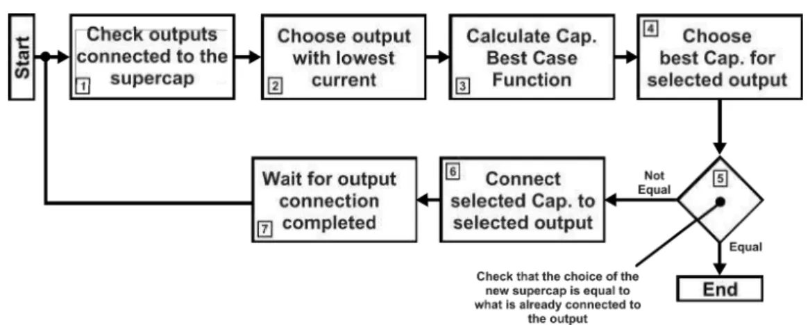
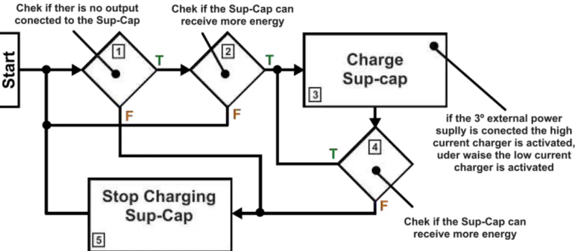
100mA. . . 41 3.14 Simplify circuits for analog signal sensing (voltage and current). . . 42 3.15 Control algorithms for evaluating the super-capacitor condition. . . 44 3.16 A second control algorithm for choosing the best super-capacitor for the output. 45 3.17 First Control algorithm, for choosing the best super-capacitor for the output. 45 3.18 Control algorithm for charging the super-capacitor to full capacity. . . 47 3.19 Computer graphical interface to visualize and control the PMU Board signals
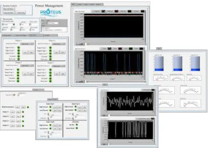
(Super-capacitor voltage, output current, switch control signals, etc.). . . 52 3.20 PMU board test setup. Consist of a load circuit to test the power output and
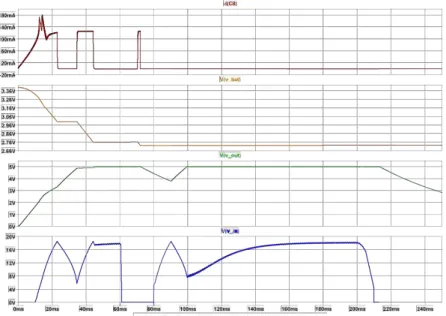
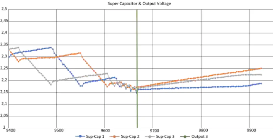
launch pad to serve as a communication interface (UART to USB) with the computer. . . 52 3.21 Experimental data retrieved from the test setup in Figure 3.20. The data
rep-resent the commutations between supercapacitors to supply power to output 3 that has an output current of approximately 100mA. . . 54
3.22 A more detailed view of the final moments of the experimental data results. The graph demonstrates the moment where the output is disconnected due to insufficient energy in the supercapacitors. . . . 55 3.23 A more detailed view of the final moments of the experimental data results
with lower configuration values than those used to obtained Figure 3.22. . . 55 3.24 Experimental data retrieved from the test setup in Figure 3.20. The data
represents the total current being supplied to the board. A percentage of this current is used by the super-capacitor chargers. . . 55
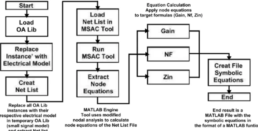
4.1 Graphical interface of the CAD software available to the user. . . 57 4.2 Main blocks of CADIT tool. . . 58 4.3 The CAD software diagram of the process to calculate the circuit equations
and it simulations for circuit sizing. . . 58 4.4 The CAD software process work-flow to obtain the symbolic equations files of
the circuit functions. . . 59 4.5 The CAD software process work-flow to obtain the NF symbolic equations files
of the circuit. . . 60 4.6 LNA circuit. . . 62 4.7 Theoretical parametric simulation of the single ended Gain equations forLmin
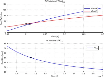
sizing. Variation ofV DsatandIDfrom CG and CS. . . 66
4.8 Theoretical parametric simulation of the Zin equation forLminsizing.
Varia-tion ofV DsatandIDfrom CG. . . 67
4.9 Theoretical parametric simulation of the NF equations forLminsizing.
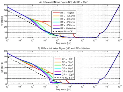
4.10 Theoretical parametric simulation of the current (relationship between the current of the CG and CS stage, n = IDCS
IDCG) influence in the NF equation for
various sizing. . . 69
4.11 CG and CS influence in the NF forLminandn= 2 sizing. . . 70
4.12 Theoretical parametric simulation of the filter influence in the NF equation forLminsizing. . . 70
4.13 Theoretical and Cadence Gain simulations and the error between them for Lminand 3Lminsizing . . . 71
4.14 Theoretical and Cadence Zin simulations and the error between them forLmin and 3Lminsizing . . . 72
4.15 Theoretical and Cadence NF simulations and the error between them forLmin and 3Lminsizing . . . 73
4.16 Theoretical and simulated with and without RF model Gain simulations for Lminandn= 2 sizing . . . 74
4.17 Theoretical and simulated with and without RF model Zin simulations for Lminandn= 2 sizing . . . 74
4.18 Theoretical and simulated with and without RF model NF simulations for Lminandn= 2 sizing . . . 76
4.19 Comparing the theoretical data (with DC simulation parameters) and simu-lated TF, of the circuit presented in Figure 4.6, in Cadence software, for weak inversion. The TF represents the gain in the differential output. . . 77
4.20 Comparing the theoretical data (with DC simulation parameters) and simu-lated Zin, of the circuit presented in Figure 4.6, in Cadence software, for weak inversion. . . 77
4.21 Comparing the theoretical data (whit DC simulation parameters) and simu-lated NF function, of the circuit presented in Figure 4.6, in Cadence software, for weak inversion. The NF represents the noise in the differential output. . . 78
5.1 Final expected result, the system is incorporated in a cylindrical container with a small opening for the sensors. . . 81
5.2 Rolling Probe structure. . . 82
5.3 ICAN prototype boards, expected result. . . 83
5.4 Rolling probe defined connections between boards (pin functionality). . . 83
5.5 Theoretical implementation (expected final result) of the complete system, ICAN Node Sensor, PCB’s stack version 1V. It’s presented four types of con-figurations. . . 84
5.6 Rolling probe first version prototype assembly. . . 85
5.7 Test setup for the rolling air probe. . . 86
A.1 Input power connections and harvester circuit. . . 102
A.2 MSP430 circuit and analog and digital signal connections. . . 103
A.3 Four output power connections and there respective DC/DC Converters. There is also present the current sensing circuits. . . 104
A.4 First super-capacitor and its chargers, its also present the voltage sensing circuit. 105 A.5 Second super-capacitor and its chargers, its also present the voltage sensing circuit. . . 106
A.6 Third super-capacitor and its chargers, its also present the voltage sensing circuit. . . 107
A.7 External power input to supply directly to the outputs. . . 108
A.8 PMU PCB layout, first tow layers. . . 109
A.9 PMU PCB layout, last tow layers. . . 110
A.10 PMU PCB silk-screen layer, top and bottom. . . 111
A.11 Message structure for OpCode 176 and 177. . . 112
A.12 Message structure for OpCode 200 and 202. . . 112
A.13 Message structure for OpCode 201. . . 113
A.14 Message structure for OpCode 203. . . 113
A.15 Message structure for OpCode 204 and 205. . . 114
A.16 Message structure for OpCode 11. . . 115
A.17 Message structure for OpCode 50. . . 116
A.18 Circuit for simulating the harvester (LTC3331) performance. . . 118
A.19 Circuit for simulating the high current power switch (TPS22918) performance. 118 A.20 Simulation for the load switch TPS22918. Its was tested withe a 10Ohmload, ans it switch from a 3.3V to a 5V power supply. The enable signal from the tow switches are overlaps. There is no drop in the output voltage, it increases form 3V to 5V. . . 119
A.21 Simulation for the load switch TPS22918. Its was tested withe a 10Ohmload, and it switches from a 3.3V to a 5V power supply. The enable signal from the tow switches do not overlaps. There is a drop in the output voltage, switch fails to make a smooth transition. . . 119
A.22 Circuit for simulating high current DC/DC converter (TPS63001) performance. 120 A.23 Simulation for the dc/dc converter TPS6001. The test was done withe 2Ohm load, and a supercapacitor withe a 5V initial voltage and 1mF capacity. The output voltage is 3.3V. The converter fails to keep the voltage stable for input voltages lower than about 3.3V. . . 120
A.24 Circuit for simulating the low current DC/DC converter (LTC3531) perfor-mance. . . 121
B.1 Final expected result . . . 123
B.2 Processing unit block, implemented using an MSP430 family device. . . 124
B.3 Communication block, implemented withe a BLE device. . . 124
B.4 Communication block, implemented withe a UNB device. . . 124
B.5 Processing and AFE unit, implemented with PSOC 5. . . 125
B.6 Data storage unit, implemented withe the use of a SD card. . . 125
B.7 Power unit, implemented using a coin cell and a dc/dc converter. . . 125
B.8 Sensor unit, implemented with a gyroscope, accelerometer, magnetometer temperature, and light sensor. . . 126
B.9 ICAN Booth for the rolling probe prototype. . . 130
B.10 Test setup, for demonstrate the prototype at work. The capsule will pass to an acrylic pipe to simulate the application environment. . . 130
B.11 ICAN poster for the rolling probe concept. . . 130
B.12 The rolling probe developer team. . . 131
B.13 The rolling probe team withe one of its adviser (Prof. João Oliveira). . . 131
B.14 Receiving the prize for second place. . . 131
3.1 High Current Charger Configuration Bits . . . 29 3.2 FLOAT Configuration Bits . . . 29 3.3 UVLO Configuration Bits . . . 30 3.4 Communication codes for UART interface send by the PMU Board. . . 32 3.5 Communication codes for UART interface received by the PMU Board. . . . 33
4.1 All, small signal, models available to the user . . . 60 4.2 Theoretical and Cadence transistor parameters for 3Lminandn= 2 . . . 75 4.3 Theoretical and Simulated with and without RF model transistor parameters
forLminandn= 2 . . . 75
A
AC Alternating Current.
ADC Analog to Digital Converter.
AFE Analog Front End.
ASIC Application Specific IC.
B
BGA Ball Grid Array.
BLE Bluetooth Low Energy.
BSIM Berkeley Short-channel IGFET Model.
C
CAD Computer Aided Design.
CADIT Computer Aided Design Integration Tool.
CG Common Gate.
CM Communication Module.
CMOS Complementary Metal Oxide Semiconductor.
CNT Carbon Nanotube.
CPLD Complex Programmable Logic Device.
CPU Central Processing Unit.
CS Common Source.
D
DC Direct Current.
DPU Digital Processing Unit.
DSP Digital Signal Processor.
E
ESR Equivalent Series Resistance.
F
FPAA Field Programmable Analog Array.
FPGA Field Programmable Gate Array.
G
GUI Graphical User Interface.
I
I2C Inter-Integrated Circuit.
IC Integrated Circuits.
IEEE Institute of Electrical and Electronics Engineers.
IoT Internet of Things.
J
JTAG Joint Test Action Group.
L
LED Light Emitting Diode.
LNA Low Noise Amplifier.
LSB Least Significant Bit.
M
MEMS Micro-Electro-Mechanical System.
MIXDES Mixed Design of Integrated Circuits and Systems.
MOSFET Metal Oxide Semiconductor Field Effect Transistor.
MSB Most Significant Bit.
N
NF Noise Figure.
O
OP Operating Point.
P
PCB Printed Circuit Board.
PMU Power Management Unit.
Q
QFN Quad Flat No leads.
R
RF Radio Frequency.
S
SAR Successive Approximation Register.
Si2 Silicon Integration Initiative.
SiP System in a Single Package.
SoC System in a Single Chip.
SPI Serial Peripheral Interface.
T
TF Transfer Function.
U
UART Universal Asynchronous Receiver/Transmitter.
UNB Ultra Narrow Band.
UWB Ultra Wide Band.
V
VLSI Very-Large-Scale Integration.
W
Z
C
h
a
p
t
e
1
I n t r o d u c t i o n
1.1 Motivation and Background
The Internet of Things (IoT) is pulling the physical and virtual objects into an ecosys-tem of global information combining advanced wireless connectivity, advances in micro and nanotechnologies, energy harvesting and storage, and more data storage and signal processing capacity. This is forcing significant changes in traditional sensor monitoring micro-systems, namely in terms of cost and flexibility. This flexibility requires the use of multiple sensor nodes capable of interact within a mesh communication network and their operation is required to be easily re-configurable. Another aspect is the management of energy and power inside the IoT, which must be designed in order to allow the opera-tion of the node with reduced maintenance cost (for example, for battery replacement).
The IoT paradigm is being introduced in many types of applications. For exam-ple, in the field of water quality monitoring, strong developments efforts are targeting its widespread use over public water networks, supported on compact and energy au-tonomous multi-sensor node probes based on low-cost sensor technologies, e.g. Micro-Electro-Mechanical System (MEMS) and Carbon Nanotube (CNT), co-integrated with a System in a Single Chip (SoC) designed in a low-cost standard Complementary Metal Oxide Semiconductor (CMOS) technology1.
The typical architecture of the IoT node consists of four main subsystems, which are the Analog Front End (AFE) module, the Digital Processing Unit (DPU), the Communi-cation Module (CM) and Power Management Unit (PMU). Figure 1.1 shows a simplified block diagram of an IoT node.
The AFE subsystem is responsible for the acquisition and conditioning of the analog
1PROTEUS project which is an European Union’s H2020 Programmed for research, technological
Figure 1.1: Diagram of the project system proposed architecture.
signals delivered by the sensors. Besides these tasks, the AFE also incorporates a high resolution Analog to Digital Converter (ADC) whose output is further processed by the digital subsystem. The latter is also responsible for the operation of the complete node. Another important block is the CM which deals with the exchange of information between the node and the Cloud based application. For the case of wireless communications, the trend now is that this module can support multiple standards and multiple radio bands, meaning that the Radio Frequency (RF) front-end must be designed accordingly. The Low Noise Amplifier (LNA), which is part of the RF front-end, plays an important role since it must have a wideband characteristic in order to support multiple radio bands. This is one of the topics covered in this dissertation, in the context of full integration either by using a SoC or System in a Single Package (SiP) approaches, in order to reduce the device size.
Another topic is the PMU which is responsible for the harvesting, storage and supply of energy to the IoT node. To improve flexibility, multi-source energy harvesting sources is a trend in the modern IoT node design. Additionally, the PMU has to be able to recognize the power requirements needed by each node subsystem and correctly manage the balance and flux of energy between the harvesters, the energy storage elements and the circuits.
1.2 Overview and Contributions
Focusing on the design aspects of the IoT node, the contributions of this thesis are divided in three areas, including circuit design optimization software, PMU and multi-sensor IoT node implementation, as briefly described in the following list:
with noise canceling, which is the first stage of a receiver in the communication block. Optimization circuit design algorithms were implemented and grouped in a single software package with a Graphical User Interface (GUI). The software allows the extraction of the transfer functions regarding the single ended and differential gain of the LNA as well as the Input Impedance (Zin) and the Noise Figure (NF), considering device noise sources and parasitics. A symbolic extraction tool and modified node analysis is used to achieve the desired outputs. This work has origi-nated a publication in Institute of Electrical and Electronics Engineers (IEEE) Mixed Design of Integrated Circuits and Systems (MIXDES) conference, entitled “Analysis of a Noise Canceling LNA using a Si2 OpenAccess based Tool - CADIT” [3].
• Design, implementation and testing of a PMU prototype capable of managing and monitoring the flow of energy between multiple energy harvesting sources (both Alternating Current (AC) and Direct Current (DC) type), multiple energy storage elements (including super-capacitors and lithium battery) and the modules of IoT node that requires energy to operate.
• Implementation and testing of a multi-sensor IoT node, designed using a modular approach for increasing the reconfigurability. The resulting implementation, des-ignated by “Rolling Probe” has received the second prize in the 2016 International Contest of Innovation ICAN’162, Paris-France.
The output of the work was partially included in the research project PROTEUS3. The existance of PROTEUS is due to the fact that “water is a vital to all forms of life (human, animal and plant) and its quality is essential to people health. It is also an unavoidable component in a wide range of industrial process, from energy production to construction activities or food production. (...) Therefore, the production of water quatity and quality is among the cornerstones of environmental protection schemes worldwide” [2]. This being said the overall objective of the project is to have an autonomous, highly multi-functional node sensor capable of monitoring drink and waste water quality in an adaptive and cognitive way, enabling a single device to support different application goals related to water monitoring networks. The final goal of Proteus is to give the roots for a full integration of all systems and sub-systems in a single SoC/SiP device.
2International Contest of innovation, shorted as iCAN. It’s globally co-organized by the iCAN
Associa-tion, ESIEE, ENS, Peking University, VDE, IEEE NTC, ANF, MEMS Park Consortium, Nano-Tera and Chinese International NEMS Society.
3This project has received funding from the European Union’s H2020 Programme for research,
1.3 Thesis Organization
This dissertation is divided into six chapters and several appendixes. The first chapter introduces the objectives and gives an overview of the main contributions. In the con-text of the IoT, the second chapter addresses the design considerations and principles of the IoT node. It illustrates the general ideas behind the work developed under the project in which this dissertation was included. Chapter three deals with the design, implementation and testing of a power and energy management prototype for the IoT node. Still in the scope of the IoT node design, the fourth chapter presents the implemen-tation of a software tool used for the circuit design optimization using nano-scale CMOS technologies. Chapter five presents the implementation of a IoT node for multi-sensor applications, as is the case of the quality monitoring systems. The last chapter presents the conclusions and future work topics. To support the main content of this document, several appendixes are included with additional information.
1.4 Software Used in this Thesis
For the development of the work done in this thesis it is necessary the use of different types of software, from simulators to editors for programming code.
In relation to the work carried out in chapter 3, that refers to the study done in the area of power management and in chapter 5, the design of a smart node, the following software’s were used:
• EAGLE from AUTODESK, it was used to design the Printed Circuit Board (PCB) of both prototypes (physical implementation of the systems);
• LTSPICE from Linear technology and TINA from Texas Instruments, they were used to simulate the behavior of several components;
• Code Composer from Texas Instruments, was used for programming C code to be loaded in the MSP430 microcontroller;
• LabVIEW from National Instruments, was used to implement a graphical interface to display data from the prototype (PMU).
For chapter 4, the development of a Computer Aided Design (CAD) tool to help in the designed of circuits, the following software’s were used:
• MATLAB and MATLAB engine from MathWorks, was used for graphical repre-sentation of data (graphics) and calculation of the node equations (modified node analysis);
• Microsoft Visual Studio from Microsoft, was used to designed, in C++, a graphical interface for control;
C
h
a
p
t
e
2
D e s i g n C o n s i d e r a t i o n s f o r t h e
M u lt i - s e n s o r I o T N o d e
2.1 Introduction
This chapter presents the main aspects to take into account when designing a multi-sensor IoT node. This chapter begins by introducing the concept of IoT, and then centers the discussion around the IoT node. A module-based architecture is advocated with special emphasis on the PMU. Finally, system integration in SoC & SiP is referred, highlighting the need for tools dedicated to circuit design optimization.
2.2 Internet of Things (IoT)
The first step into what is known today as the IoT was the concept of the Wireless Sensor Network (WSN) which is defined as “A Wireless Sensor Network can generally be de-scribed as a network of nodes that cooperatively sense and may control the environment, enabling interaction between persons or computers and the surrounding environment”, [26]. The WSN are constituted by “node sensors and actuators”, which may include a gateway to bridge to a different network or to connect to a user/client, as demonstrated in figure 2.1. Usually the network contains multiple nodes with a random distribution within an area in which it is desired to monitor. Advanced techniques of self-adaptation and self-organization were proposed in the past to improve not only the interconnectivity and interoperability between nodes but also to optimize the overall energy consumption of the entire system, [34, 48].
Figure 2.1: Wireless sensor networks.
object can connect to the Internet and share information with other devices, similar or not, to supply and access all of real-world information. With the increased use of various types of sensors and the potential massive information data, there is now a need to connect all of these IoT nodes to Cloud scaled technologies (processing, storing data) using the services provided by the Internet. This is now possible due to advances in wireless communications, distributed computation process and fast speed Internet, [38]. In fact, objects with sensors, actuators and controllers can now be connected to the Internet and controlled remotely, linking the physical world to cyberspace through the smart device. Everyday object can now be an extension of the Internet into the real world,[4], [20]. The potential of IoT spreads in a large variety of applications, namely ([4, 8, 20, 32]):
• Smart Home/Smart Building, to improve energy efficiency and smarter home envi-ronments;
• Health-care and Wearables, as for example in the case of elderly care;
• Smart Environment Monitoring/Smart Cities, namely for monitoring and control traffic flows, city logistics, water quality monitoring and rational use of water re-sources;
• Security and Safety.
2.3 The IoT Node
• The power management module is responsible for provide a reliable power supply to the node;
• The sensor allows the node to acquire information about environmental and equip-ment status. It is responsible for collecting and conditioning the signals, such as light, vibration and chemical signals, into electrical signals;
• The micro-controller processes the digital/analog signals coming from the sensors units;
• The wireless transceiver (RF module) provides the bidirectional connectivity with the Cloud application.
Figure 2.2: Node sensor architecture.
It is necessary to take into account the importance of node features of tiny size and lim-ited power in the design of all components of the sensor network [10, 23, 26]. As reported in [27], it’s possible to identify slightly differences in the way the sensor architecture is built:
• based only on a Micro-controller,
• based on Digital Signal Processor (DSP),
• based on Application Specific IC (ASIC),
• based on programmable hardware devices (Field Programmable Gate Array (FPGA) or Complex Programmable Logic Device (CPLD)),
• using Field Programmable Analog Array (FPAA),
• based on SiP or SoC,
2.3.1 Sensors
The most common type of sensors are fabricated in discrete packages being some of them inexpensive and easy to use. However, with the need of small form factors nodes, it is necessary to co-integrate the sensors along with the SiP or SoC. With the miniaturiza-tion technology based on MEMS, it is now possible to combine microelectronics with micro-machining technology in 2D or 3D micro-packaging structures. Integrating these structures with power harvesting supply and signal conditioning circuits we obtained miniature MEMS based node sensors. At present, there are already many types of minia-ture MEMS sensors in the market which can be used to measure a variety of physical, chemical and biomass signals, including displacement, velocity, acceleration, pressure, stress, strain, sound, light, electricity, magnetism, heat, pH value [11, 14–16, 25, 26].
2.3.2 Connectivity
The IoT node can now select a variety of communication standards, with some of the most used highlighted below:
• Bluetooth Low Energy (BLE),[12],
• ZigBee, [17],
• Ultra Narrow Band (UNB),
• Ultra Wide Band (UWB),[7].
One of the criteria for the choice of a transceiver is the coverage range for a given trans-mission type attending to the energy available at the node.
2.3.3 Energy and Power Management
Power management is the most important aspect of sensor node. It is responsible for supplying the energy to the entire node. The energy problem in a sensor node is that there is not always enough energy available, especially if the system uses only the energy supply via batteries. Therefore, to be autonomous the node energy paradigm has to change in the sense that it needs to harvest and store locally energy form the environment. As a consequence, the IoT node must be able to manage its energy consumption by applying a smart energy-saving mechanism to become efficient and prolong the life operation of the node, [19]. A sensor node can benefit from using techniques like scheduling their operations in time, when there is not sufficient energy to maintain the continuous operation of all subsystems, [36].
the wireless radio channel, but not to send or receive any sensor data, while a sending state is only activated when there is useful data to be transmitted. Outside of these states, the module is in sleep mode (ultra-low power consumption). Also, to reduce the node energy consumption we can reduce the communication time, reduce the traffic (through data compression to reduce redundant data sent) and reduce the transmitted power of the sending node, [13].
2.3.3.1 Energy Harvesting
The use of energy harvesting gives the ability to node sensor to extend their operating live, [28]. As reported in [7, 26] “Ambient energy harvesting cannot only be realized by conventional optical cell power generation, but also through miniature piezoelectric crystals, micro-oscillators, thermoelectric power generation elements, or electromagnetic wave reception devices”. Two types of energy harvesters, [13] are:
• Vibration energy is obtained by the use of piezoelectric materials. By applying a force, the material deforms which produce a polarization charge that can be used to extract energy;
• Solar energy through the use of advanced photoelectric technology can operate both indoor or outdoor and they are lightweight and easy to install.
There are two major approaches in how a system may collect and use the energy of the environment in which it will be inserted [39]:
• Harvest-Use Architecture: the energy harvested is directly used by the the sensor, this means that it can only operate if there is available power continuously over a level that allows their operation, otherwise the node crashes due to insufficient power.
• Harvest-Store-Use Architecture: energy is stored before being used which allows the node operation when the harvester is not available to to provide power.
2.3.3.2 Energy Storage
The combination of energy harvesters with energy storage elements is a key principle to obtain an autonomous IoT node, [39]. Sensor nodes can benefit from two main types of storage elements: battery and super-capacitors.
Batteries are expensive and have a limited useful life (limited number of recharge cycles), has however high output voltage, high energy density, and moderately low self-discharge rate. They may also need special charging circuits which increases the complex-ity of the system design. Two storage technologies, NiMH and Lithium based, emerge as good choices.
power source, a rectifier is needed. One disadvantage is the fact that the supercapacitor self-discharges at a much higher rate than battery, [49]. The advantage that have influ-enced the use of supercapacitors is its much higher power density and low Equivalent Series Resistance (ESR). Also, a typical supercapacitor supports a much higher number of charging cycles, [37].
2.4 Design considerations
Due to the increasing integration of IoT systems into an enormous diversity of appli-cations, each with different characteristics but requiring the same electronic platform (sensor node), it is necessary to look for systems capable of following the requirements that IoT requires.
For this, each sensor node must have three main characteristics:
• Processing capacity, that allows the control of all aspects of the system and imple-mentation of algorithms for signal processing;
• Ability to read the physical world (using sensors);
• Autonomy, being active and function properly for long periods of time without any intervention needed.
2.4.1 Analog Front End (AFE)
The AFE establish the interface between the sensor and the digital part. It comprises sensor biasing, sensor signal readout and conditioning and an ADC.
2.4.1.1 Sensor Biasing
The analogue interface for sensing the physical environment needs to adapt to the diverse characteristics of the sensors. Most analog sensors need to employ some method of biasing (for establishing proper operating conditions), and this varies from sensor to sensor. In order to have some control over that parameter a biasing interface (polarization circuit) is needed that can generate variable voltages or currents. For this, the use of Digital to Analog Converter (DAC) is employed.
In most sensors the biasing can be used to define the range of values to be read. If the value is greater than the limits of the ADC it is possible to adjust the biasing, as demonstrated in figure 2.3. This method provides the use of a single biasing circuit for multiple sensors through multiplexing.
(a) Different biasing for the same resistance. By
applying different biasing current to the same
resistor, the output voltage can be increased or decreased.
(b) Different biasing for the different resistance.
By applying different biasing current to diff
er-ent resistors, the output voltage is the same for all.
Figure 2.3: Biasing graphics (sensor output amplification).
(a) Current biasing method. (b) Voltage biasing method.
Figure 2.4: Polarization circuit for resistive sensors.
It’s possible to use two types of biasing circuits, either using current or voltage, as shown in the figure 2.4. The current biasing is preferred because it requires less com-ponents and is independent of parasitic resistances between the biasing source and the sensor. In other words, there is more freedom in circuit layout design (there is a relax-ation of the interface layout restrictions with PCB sensors, connector type, track size and track spacing).
The method of voltage biasing requires, for sensors with very different internal resis-tance characteristics, the need to re-size the biasing resisresis-tance if the ranges of variation are either very small or very large, as demonstrated by the equations 2.1a for the extreme cases,
VOut=
RSensor
RSensor+RBias
!
·VBias (2.1a)
VOut≈ RSensor
RSensor
!
·VBias≈VBias , RSensor≪RBias
VOut≈0·VBias≈0 , RSensor≫RBias
(2.1b)
all sensors. This may involve excessive energy consumption in extreme cases. Another option is to keep the value of the voltage variable, but to introduce a biasing resistance for each sensor in which its sizing will be according to the characteristics of the sensor in question. However, this option implies N resistors for N sensors (using a analog multi-plexer between the biasing circuit and the sensor), resulting in a larger implementation area and layout complexity.
Using the current biasing method shown in the figure 2.4a, it is possible to reduce the layout area, the complexity of designed and the energy consumption. The extreme cases where there are large differences between sensors, is now simpler to deal with, only a current DAC capable of generating the necessary interval of biasing values is essential.
VOutsensor =Rsensor·IBias (2.2)
For a given range of variation of the internal resistance value of a sensor, it is possible with increasing or decreasing, through the equation 2.2 (linear equation whereIBias deter-mines the scale of the range of values to be read), to increase or decrease the value range (if the range of values is small by increasing the biasing these values will be amplified by a factor ofIBias, as shown in the figure 2.3).
2.4.1.2 Sensor Multiplexing
As previously described with the implementation of a variable biasing circuit, it is possi-ble to excite several sensors through a single biasing circuit. For this, the integration of an analogue Multiplexer (MUX) (implemented with analog switches) is employed. Thus, allowing a reduction of layout area and low consumption, since the MUX consumes less than N biasing circuits. The number of sensors is now limited to the size of the MUX, allowing the implementation of a single sensor node capable of measuring all the sensors required for a particular application.
However, the use of MUX presents some disadvantages, being, the excitation and measurement of one sensor at a time, the intrusion of parasitic effects such as the internal resistance of the MUX switches, for high frequencies the maximum bandwidth in the signal can be reduced and also a noise source can be introduced.
2.4.2 Processor Unit
A node sensor needs to have a processing unit in order to implement communication and control protocols on all the re-configurable aspects of the system. It is necessary to implement smart controls, such as power management, and to implement, if necessary, some signal pre-processing, in order to reduce the amount of information to be shared.
part of the whole system implemented and integrated in a single chip, thus reducing the number of components in the implementation. This solution does not require any devel-opment in the integration and analog and digital subsystems. Some micro-controllers are used for low power applications in which they exhibit low power consumption modes. The development of applications in this type of system, is all the basis of configuration of the registry of its peripherals (through programming).
The use of FPGA in the designed sensor node as the processing unit requires additional steps, being a more difficult solution and time consuming to implement. Unlike the micro-controllers in which the system is implemented, in FPGA it is necessary to implement the logic of the processor. FPGA thus allows greater re-configurability in the digital part, since the processing unit can now be customized according to the needs of the applications. It also implies the opportunity to develop hardware accelerators where a Central Processing Unit (CPU) intervention is not necessary. FPGA also has the advantage of being able to implement multiple controllers independent of each other.
Unfortunately, in applications where it is necessary to use sensors, the FPGA can only be used for the digital part of the system as it does not offer integrated analog blocks, these blocks will have to be added externally if necessary.
2.4.3 Power Management
Consumption and storage of energy is one of the main problems in autonomous sensor nodes. The amount of energy is limited and there are no continuous sources of energy for high power consumption, what implies that there must be strategies to lower con-sumption. This must be well managed according to the needs and requirements of the application and systems that minimize energy waste, such as the use/implementation of circuits optimized for low power applications.
The use of alternative energy sources should be used to supply energy storage tanks whenever possible using methods that allow the collection of energy from the environ-ment to the system (e.g. solar energy collection), i.e. the use of renewable energy sources should be used to maximize the collection of energy from all possible sources of energy present in the environment in which the system is inserted (ex. solar energy together with energy from vibration through a piezo).
Because of the rapid use and storage/harvesting of energy, i.e. charging and discharg-ing, of conventional energy storage media (batteries), they are no longer able to deal with this type of operation, their wear is very high, they have limited number of charging cycles. It is necessary to think about new strategies.
handle the stress of multiple loads whenever there is energy to harvesting and space for store it.
However super-capacitors have a very high self-discharge, much higher than a battery. The ideal would be to use a combination of the two. Fast consumption (small charges and discharges) can be carried out on the super-capacitors (the capacitor is always being charged and discharged) and when prolonged consumption is required, which means longer charges, the batteries are used because they can have a higher energy stored than a capacitor. Thus, the stress of rapidly charging and discharging is mainly in the super-capacitor, that can handle this effect better.
It is also possible to use more than one super-capacitor. This allows a longer duration in the power supply for a certain task, resulting in a lower use of the energy of the batteries, consequently reducing the number of charges to it. It also implies that while one capacitor is supplying power, the others may be charging whenever it’s possible the energy storage (there is still storage space and energy available to store). And it allows several tasks to occur at the same time within the limits of energy stored in each super-capacitor.
2.4.3.1 Super Capacitor Charging
The use of super-capacitors is useful for storing small amounts of energy to be used quickly. For this purpose, it is necessary to use some method to charge the capacitor with energy, which is fast and efficient. Two ways to charge a capacitor were considered, through a voltage source or a current source.
Charging using a voltage source
With the charging voltage source, it is necessary to introduce a resistor in series with the capacitor as shown in figure 2.5b. This is because, if the connection of the voltage source is made directly to the capacitor, there is no control over the maximum current occurring in the same (maximum current theoretically will be infinite1).
In reality there is always a resistance between the voltage source and the capacitor (internal resistance of the source and capacitor terminals and the resistance of the con-ductors between the two), but this can present very low values which is nonetheless problematic, because the current is of very high values due to the fact that the capacitor has a high capacity. Whit high values of current this can mean the destruction of the super-capacitor, the power supply and the connections between the two (e.g. connection lines of a PCB).
1The capacitor behaves as a short circuit at the beginning of charging. That is, at the terminals of the
capacitor at timet= 0 (when charging starts) there is a discontinuity in the voltage at its terminals, going
from zero Volts to the voltage ofV1. Using the current equation in a capacitor, the derivative of the voltage
(a) Charging behavior. Blue line represents the voltage across the capacitor terminals and the orange line represents the current entering the capacitor.
(b) Charging circuit. Consists of a voltage
source in series with a resistor and a capacitor.
Figure 2.5: Circuit and graphic behavior for voltage charge method.
The capacitor voltage and current equations of the circuit in figure 2.5b were taken from [31]. It is possible to verify both by the figure 2.5a and by the voltage equation 2.3 and current equations 2.42that the charging behavior of the capacitor is not linear (have exponential components),
VCapacitor=V1−(V1−V0)·exp
−t
R·C
(2.3)
ICapacitor=
V1−V0
R ·exp
−t
R·C
(2.4)
This means that as the capacitor is being charged, the charging process of transferring energy will lose force, i.e. the current decreases as the voltage increases. The voltage across the capacitor when the charging time approaches infinity, tends to a value equal to that of the power source.
The charge time of the capacitor is given by equation 2.5 (from equation 2.3),
t= ln V1−V0 V1−VCapacitor
!
·R·C (2.5)
Charge using a current source
The current charging method involves applying a current source in parallel with the capacitor, as shown in the circuit present in figure 2.6b.
2These equations are drawn from the circuit analysis using the Kirchhofflaw method and rearranging
them in order to obtain a first-order differential equation with constant coefficients to be able to apply the
(a) Charging behavior. Blue line represents the voltage across the capacitor terminals and the orange line represents the current entering the capacitor.
(b) Charging circuit. Consists of a current
source in parallel with a capacitor.
Figure 2.6: Circuit and graphic behavior for current charge method.
Using the equation that defines the current in a capacitor and imposing a constant current, we obtain an equation of the current where the derivative becomes a difference between two values of voltage in a certain time interval3as shown in equation 2.6,
ICapacitor=C·
dV
dt I→.Constant⇔ ICapacitor=C·
∆V
∆t (2.6)
Through the use of equation 2.6 and rearranging the variables and assuming that the time interval is between the initial instantt0= 0 up untilt, the voltage equation 2.7 is obtained , where V0 Is the value present in the capacitor at the initial time (start of charging),
ICapacitor=C·
∆V
∆t ⇔ICapacitor=C·
V0−V
t ⇔V =V0+
ICapacitor C
!
·t (2.7)
It is possible to verify in the figure 2.6a and in the equation 2.7 that the voltage in the capacitor (the charging of the capacitor) now has a linear behavior. The voltage equation now shows the shape of an equation of a line in which the slope of this is given by the relationship between the current and the capacity of the capacitor (ICapacitor
C ).
The time that the capacitor takes to be charged to the desired value is given by equa-tion 2.8 (from equaequa-tion 2.7),
ICapacitor=C·
δV
δt ⇔ICapacitor=C· V0−V
t ⇔t=C·
V0−V ICapacitor
(2.8)
Theoretically the charging method by current causes, if the charging time is infinite, the voltage in the capacitor to be infinite. But in practice, because a current source is
3If the currentI
Capacitoris constant, the integral of the current in the capacitor has as an equation, that
of a straight line,
ICapacitor=C·dVdt ⇔V= Z 1
C·ICapacitordt⇔V=∆t·ICapacitor·
1
C+V0⇔∆V=
normally constituted by active elements such as transistors, if the voltage in the capaci-tor causes voltages ofvds(transistor Metal Oxide Semiconductor Field Effect Transistor (MOSFET), drain to source voltage) smaller than vdsat (transistor MOSFET, drain to
source saturation voltage), they are no longer able to generate current, thus limiting the voltage in the capacitor.
Comparison
It’s demonstrated in figure 2.7 the simulations of the two charging types of circuits present in figures 2.6b and 2.5b. In the two types of circuits here demonstrated the size of the capacitance in them is the same and the size of the resistance is obtained in order to maintain the initial current equal for both circuits.
Figure 2.7: Electrical simulation of current and voltage charging schemes for the compar-ison of the behavior of the circuits in Figures 2.6b and 2.5b.
For a charging with the same characteristics as the initial current and maximum voltage on the capacitor, using the current method becomes faster, because the current with the passage of time does not decrease as the capacitor voltage increases, as expected in the charging voltage method, i.e. does not lose the charging force, remaining constant. For the same characteristics, the current charging method reaches the maximum voltage value when the voltage charging method is still only 63,2%4.
The use of constant current to charge the capacitor also has an impact on is control, as the equations are linear (equation 2.6) it’s less expensive, in energy and time, to calculate in processing units (CPU, micro-controllers). Thus resulting in faster and more efficient
4The time constantτ=R·C represents the time the capacitor takes to charge if the current remains
constant. Replacingτin the equation 2.3 and assuming that the initial value is zero, we obtainVCapacitor=
controllers (fewer operations are required than to calculate the exponential equations 2.4 e 2.5).
2.4.3.2 Programming Techniques
The storage of energy may not be enough for a given application to keep all its func-tionality active, such as communication and sensor reading, among others. But it has to be at least enough to keep at least one at a time for a limited period of time. It is thus important to apply some scheduling of the various tasks present on a node sensor, that is, only one thing is done at a time. In a sensor node with many peripherals only those whose scheduled task is required to perform their functions are connected.
If the processing unit has features that allow the energy consumption to be reduced, they should be used whenever possible. Some functionalities are:
• the use of several types of operating modes, where it is possible to put the CPU and its peripherals when they are not being used in standby (the peripherals are powered offuntil needed),
• the use of interrupts to generate events that wake the CPU when something impor-tant happens (as some kind of stimulation at the terminals of a micro-controller).
In a controller program design, it must be implemented to operate at base events (interrupts, which can be triggered by internal or external peripherals), where the CPU and peripherals are only active when needed. If some kind of delay is needed this should be done with timers, as they allow the CPU to be offwhile waiting (only the timer is on), i.e. the CPU will not be blocked counting the delay time.
In programming micro-controllers, events are triggered by interrupts, but as some events may share multiple interrupts 5 these should be kept as simple as possible so as not to block the CPU for a given interrupt stimulus. It should be noted that the use of calculations in events should be used as little as possible, especially if they are complex calculations. These types of calculations can take a long time to be calculated causing some triggered interrupts to not be taken care of (the event is lost). It is good practice to keep the calculations and complex functions inside the main function of the program (main function, in C code), this allows to release the subroutine for new interrupts, because calculations or functions can be interrupted.
2.4.4 Software Tools for IoT node circuit design
With the tremendous demand for increasingly faster wireless communication, the level of specifications in terms of noise and bandwidth are increasingly difficult to achieve because it’s necessary for greatest debit of bits, greater robustness between signal and
5Event is a subroutine that is called whenever an interrupt is triggered, the combination of multiple
noise and higher bandwidth, thus originated receptors (Front End) increasingly difficult to implement.
One of the main blocks of a Front End, probably the one with the most important and difficult design constraints to achieve, is the LNA. The restrictions of a LNA are due primarily to noise introduced in this system. The noise of this block, as is the first in the signal path (directly coupled to the antenna), is what has the greatest impact on the final Front End noise. The gain of this block is also important because the noise of all the blocks after the LNA are divided by this gain, thereby reducing the effect that these have on the Front End. Another constraint is that the Zin of the LNA must have specific value in order to have an adapted antenna,
As these days the use of different carriers for different types of communication in one device requires that the equipment is capable of receiving signals over a wide bandwidth. The use of a wide band LNA allows the receiver to have only one LNA for all carriers thereby reducing the chip size and power of the same.
Due to the high cost of making the layout masks of the circuits, it’s necessary to know before production the circuit performance, so if there is something wrong (specifications not achieved), it can be possible to correct the error in time before it’s construction thus saving money and time. To be possible to predict the circuit operation is necessary to obtain the equations that model the circuit characteristics (gain, Zin, NF). Making the extraction of this equations by hand, is not trivial and can be time consuming. So, in order to obtain these complex equations, with some precision, we turn to CAD software to simplify this process. This types of software’s can be simulators, like Cadence Virtuoso and Ngspice, among others.
The use of CAD software makes possible a complete and accurate (depending on the modulation of the instances) theoretical analysis of the circuit, reducing the time and cost of circuit design.
2.4.5 Conclusion
The design of a system, to be integrated in IoT, propose a serious growth in complexity, to maintain is operation across several applications without the need to redraw the system. It is necessary to increase the operating time in which the system is active and the ability to self-adapt its functionalities to various applications.
For the power management of a system a good strategy can be the use of supercapac-itors as alternative energy storage units, using the constant current method for energy transference, due to the fact that this one is faster. However, to improve power consump-tion, methods such as using interrupts in software, allowing the CPU to be turned off when it is not needed, can improve the energy consumption, allowing to extend the time in which it is active. Using energy harvesting from the environment when possible can also extend the time of operation.
required, it’s necessary the used of components like FPGA and microcontrollers that have the ability to be reconfigurable, like for example the used of an ADC form a microcon-troller that requires the application to measuring signals from sensors. Also, to increase reconfigurability to measure several types of sensors the use of a MUX and current biasing are beneficial. Current biasing allows for the AFE to adapt is range, to the requirements of the sensors.
C
h
a
p
t
e
3
Po w e r M a n a g e m e n t U n i t
Figure 3.1: PMU Board (theoretical representation).
3.1 Introduction
The ability to connect and disconnect parts of the system circuits (and also to choose its power source) allow to decrease unnecessary energy consumption, do with the fact that, these circuits are completely disconnected and do not have any current consumption, as would be, if they were in standby (always have a small amount of current being used). In order to be able to connect and disconnect sub circuits efficiently, same processing capability is necessary to implement power management algorithms.
Having the capacity to gather energy from its environment gives the system au-tonomous operation capability, meaning that the system has the ability to operate in remote locations for long periods of time. Increasing the amount of energy sources from which the system can collect energy, increasing its operational time interval. A lot of this energy sources are not constant and have periods of time where they don’t give enough energy to maintain the system operation, so the use of energy storage devices is necessary. The more storage devices the system has, the more energy it can collect, taking the maxi-mum advantage of the periods of time in which the power sources have the energy to be collected.
The normal way to implement storage elements is using batteries, but a problem is presented using this strategist. The batteries have few charging and discharge cycles, meaning that, when they are used in energy harvester, they will be in a constant process of charging and discharging (energy source is not constant) this translates in a faster battery degradation. A possible solution is to implement the energy storage elements with the use of supercapacitors, these elements have a much higher number of charging and discharging cycles. Unfortunately, supercapacitors have lower energy storage capabilities, in comparison with batteries, so implementing an array of capacitors is necessary to increase storage limits. If we also maintain each of the elements of the array independent of each other, we can charge some of them while using the others to supply energy when and where is needed.
In this chapter it’s presented the design and implementation of a system, for evaluat-ing the use of a supercapacitors array, energy harvester, power distribution and overall control (power management control algorithms). A PCB prototype is developed to test all these characteristics in combination with which other in a real environment. The struc-ture of this chapter consists of five sections. The first section is a brief introduction to the topic, the second section describes the system structure and its main blocks, the third section demonstrates the implementation of the system and the prototype, the fourth section presents the test results obtained with the prototype and finally the fifth section contains a small conclusion of the work done in this chapter.
3.2 System Structure
its parameters, to a controller and understand them. Which means that the system must have additional and sufficient specific hardware to manage power consumption, distribu-tion, harvesting, storing and system efficiency.
The design starts by defining the structure of the system capable of having multiple energy storage units, multiple output power rails, that can be activated or deactivated in real time and a configurable power distribution path (power MUX) between energy harvesting, energy storage and the output. This path is also controlled in real time, meaning that a processor unit is required.
Figure 3.2: PMU board block diagram (representation for power, digital and analog sens-ing signals).
The system structure main blocks consist of Energy Harvesting, Power Multiplexer, Super-capacitor, super-capacitor Charger, DC/DC Voltage Regulator and a controller. The structure of the system is presented in Figure 3.2.
The energy harvester block is responsible for collecting all the energy available from various energy sources, such as a solar panel. The management of internal power in this block is left to the LTC3331 chip from Linear Technology company [33]. This block is what provides all the energy that will be used within the total system.
Supercapacitors are the energy storage elements of this system. The energy supplied by the energy harvester is stored in these through the super-capacitor charger block im-plemented using the chip LTC4425 from Linear Technology [30]. The use of the charger blocks in the energy storage of the supercapacitors, allows to control the charging of the same ones efficiently. The charger works basically as a constant current source, thus allowing a linear behavior, easily predictable and a faster charging, as described in the Chapter 2 (Section 2.4.3.1).
allow it to be charged more quickly, this is especially useful when the super-capacitor is completely discharged, which originates long charging periods.
In order to be able to transfer energy between the supercapacitors and the outputs it is necessary to implement a block capable of receiving energy from several sources and directing them to various output. Using a MUX capable of dealing with high power levels we get a fully configurable block in which you can choose which input connects to an output, allowing each output to receive power from one source or several and the reverse is also possible.
Using supercapacitors to supply power directly into the output presents a problem because the output voltage needs to be stable (always having the same value), this does not happen in the voltage to the terminals of the super-capacitor, which decreases depending on the energy that the super-capacitor provides (supplying power to the capacitor is discharging). In order to counteract this effect, it is necessary to add a DC/DC converter that allows the voltage to be maintained stable in the output, regardless of the input voltage. So, the DC/DC block functions as a buffer that stabilizes the voltage between the super-capacitor and whatever circuits are connected to the output.
The final block is the controller. This one allows the system to be autonomous, and to have the possibility of employing intelligent control algorithms for the control of energy distribution and storage. To implement this block, it is necessary to use processing units for signal control (enable signal of the power switches, enable signal of the charger, etc.) and analogue measuring units, where the measured analog signals represent the state of the system (voltage in the supercapacitors, output current and charger output current). The best option to implement the controller block is to use a micro-controller with the ability to measure analog signals, thus being a compact and easy implementation solu-tion. The controller will be implemented using a low power micro-controller chip called MSP430FR5994 of the MSP430 family from Texas Instruments [40]. The controller will also allow for the integration of the PMU in the complete system, meaning it can interact with higher level systems throw serial communication.
3.3 System Implementations
The implementation of the system is done in two parts, the first part is hardware and the second part is software (control algorithm). The first part, within the scope of this document, is the most relevant for the study of the improvement of power management in a given generic system. Emphasis is given to the circuit design of each block discussed in section 3.2. The second part being not only to demonstrate that the circuit allows to implement an algorithm, but serves to control the control signals in each block for testing purposes.
(a) Top view. (b) Bottom view.
(c) PCB layout, 4 layers. (d) Organization and position of diagram mainblocks (Figure 3.2) main blocks.
Figure 3.3: Theoretical implementation, expected final result of the complete system (PMU Board - PCB Version V1).
be interconnected with other systems capable of performing those additional functions, this system is only concerned with dealing with power. This means that it will also be necessary for this system to have an interface which enables the ability to communicate with other systems, so that the system can be integrated into a generic application.
The expected final result of the physical implementation of the system (prototype) is presented in Figure 3.3. The physical implementation of the system involves the design of a PCB that contains the implementation of the circuits of the main blocks shown in the Figure 3.2. The physical position of the blocks in the PCB can be seen in Figure 3.3d.
3.3.1 User Interface Description