European Association for the Development of Renewable Energies, Environment and Power Quality (EA4EPQ)
International Conference on Renewable Energies and Power Quality (ICREPQ’10)
Granada (Spain), 23th to 25th March, 2010
An Improved Electronic Circuit for Tracing the I-V Characteristics of
Photovoltaic Modules and Strings
Vicente Leite
1and Faustino Chenlo
21
Polytechnic Institute of Bragança, School of Technology and Management Campus Santa Apolónia, apartado 1134, Bragança, Portugal
CIEMAT, Research Centre for Energy, Environment and Technology Av. Complutense 22, Madrid, España
Abstract.
This paper presents an improved electronic circuit for testing photovoltaic (PV) modules or strings by tracing their I-V and P-V characteristics. It consists of an electronic fast varying load based on a power MOSFET controlled by means of an innovative sweeping gate-source voltage in order to improve the tracing of the I-V characteristics on an oscilloscope. In order to prevent damage of data acquisition systems and mainly for use with high voltage PV strings, galvanic isolation is introduced for the sweeping signal as well as current and voltage measurements. In spite of this improved characteristics, the developed electronic circuit keeps the advantages of low cost and simplicity. Experimental results obtained with the electronic circuit are presented.Key words
Photovoltaic modules, current-voltage characteristics, electronic load, fault diagnosis.
1.
Introduction
Photovoltaic (PV) energy is booming. The growth of the annual market regarding PV industry was evident in many countries as support programmes began to take effect [1]. Installations of PV cells and modules around the world have been growing at an average annual rate of more than 35% since 1998 and, by the end of 2007, the cumulative installed capacity of all PV systems around the world had surpassed 9,2GW [2]. Moreover, the capacity of annually installed PV systems would reach 281GW by 2030. By analysing these two reports [1] and [2], it becomes evident that one can expect a very strong transformation and expansion of the PV industry sector over the coming decades. Considering the advanced scenario presented in [2] the average growth rate in the periods of 2007-2010, 2011-2020 and 2021-2030 will be respectively 40%, 28% and 18%. Even in a moderate scenario
the average growth will be 30%, 21% and 12% in those periods.
In spite of their well known reliability, some PV modules degrade or even fail when operating outdoors for extended periods and that can occur in a number of ways [3]. In cells’ degradation diagnosis of PV modules or arrays, the current-voltage (I-V) characteristics are usually used as well as parameters obtained from them like short circuit current (ISC), open-circuit voltage (VOC), maximum power (Pmax) and fill factor (FF=Pmax/ISCVOC). On the other hand, the I-V characteristics can be monitored and the results used to investigate and compare the actual power produced by modules under realistic operating conditions [4]. Thus, I-V characteristics are not only used by designers in power converter systems, but also in PV system design to make systems more cost effective.
Manufacturers of PV modules provide the I-V characteristics and the main parameters under the well known Standard Test Conditions (STC: 1000W/m2 of irradiance, 25ºC cell temperature and air mass 1.5). However, PV modules experiment field conditions very different from those standard ones.
Photovoltaic modules are usually tested using electronic dc loads, which can vary the resistance (load) over the entire range in a very short time. However, the ones available on the market are often expensive. Anyway, by using quite simple and much cheaper circuits, it is also possible to build an electronic dc load taking advantage of a suitable operation of a power Metal-Oxide-Semiconductor Field-Effect Transistor (MOSFET). In fact, a power MOSFET operating in its active region and mounted on a heat sink to dissipate the power, if necessary, can be used as an electronic load to test PV modules [4] – [6].
electronic circuits that facilitate the data acquisition of I-V characteristics of PV cells were proposed. The I-V characteristics of PV modules were measured in [8] with a swept method by charging a capacitor. In [4] it is reported the design of a low-cost measuring system used to monitor the I-V characteristics of PI-V modules. The system was previously developed in [9] and measures I-V characteristics of seven different modules sequentially by selecting a module through mechanical relays. Other set of relays are used to select a parallel combination of resistors used as resistive loads for a particular I-V pair of values. By using a combination of resistors, several resistances are achieved to measured I-V pairs. A more interesting electronic circuit, being a fast varying load, is presented in [6]. The circuit is based on a MOSFET operating in its linear region and the proposed circuit traces the I-V and P-V characteristics of PV modules by quickly scanning the load by sweeping the VGS (gate to source voltage) of the MOSFET with a sinusoidal waveform. Other parameters are also provided. The power generated by the PV module is dissipated in a series power resistor. In this paper an improved electronic circuit is presented to test PV modules by tracing their characteristics. As in [6] it is based on a power MOSFET but the power is dissipated in a heat sink in which the MOSFET is mounted. Moreover the scanning voltage (VGS) is achieved in an innovative way in order to improve the I-V tracing on an oscilloscope. Furthermore, galvanic isolation is introduced for the scanning signal as well as the current and voltage measurements. This is important to prevent damage of data acquisition systems and mainly to enable the circuit to be used in tests with PV strings and not only with modules. In this case, the protection of the equipment and operators is mandatory. In spite of this improved characteristics, the developed electronic circuit, as a fast varying dc load, keeps the quite simple design and low cost advantages.
2.
Principle of Operation
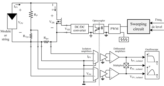
The basic circuit utilized to test PV modules using a MOSFET as an electronic load is shown in Fig. 1. VGS is the gate-source voltage, VDS the drain-source voltage and ID the drain current of the MOSFET. VPV is the output voltage of the PV module, IPV the output current, ISC the short circuit current and VOC the open circuit voltage.
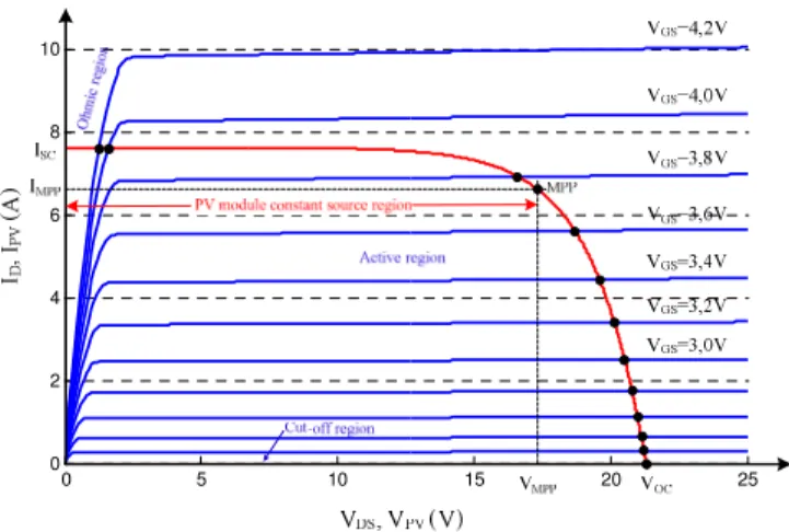
The characteristics of a MOSFET are shown in Fig. 2 where each curve ID-VDS (blue curves) was drawn for a given
gate-source voltage (VGS). The IPV-VPV characteristic of a PV module at STC is also shown in Fig. 2 (red curve). In fact, as the currents ID and IPV are the same, the operating point is given by equalizing the current of the MOSFET which is given by
(
)
(
GS th DS DS)
(
GS th)
D K V V V V KV V
I = 2 − − 2 ≈2 − (1a)
(
GS th) (
DS)
D KV V V
I = − 21+λ (1b)
and the current of the PV module which is given by
diode L
PV I I
I = − (2a)
where
−
= T 1
PV
nV V O
diode I e
I (2b)
Equations (1a) and (1b) are valid in the ohmic region (also referred as triode region or linear region where
th GS
DS V V
V < − ) and active region (also referred as saturation region, where VDS>VGS−Vth), respectively [10]. K and λ are device parameters and Vth is the threshold (gate) voltage. IL is the light-generated current (=ISC) and Idiode given by (2b) is the ideal diode law where IO is the dark-saturation current, n is the diode ideality factor (a number between 1 an 2) and VT the thermal voltage [11].
Thus, the operating point corresponds to the intersection of the PV module characteristic with the MOSFET one for a given voltage VGS. By sweeping VGS with a suitable signal the operating point of the MOSFET sweeps the IPV-VPV characteristic between VOC and ISC. While VGS is less than the threshold voltage Vth, the MOSFET will be OFF. When VGS is increased above Vth, the device will operate in its active region where ID rises approximately in a linear way with VGS.
As far as the PV module is concerned, for VPV higher than
the voltage at the maximum power point (VMPP), the
characteristic will be similar to a voltage source one. At voltages below VMPP the PV module will behave as a current
Fig. 1. Basic circuit for testing PV modules using a MOSFET as an electronic load.
0 5 10 15 20 25
0 2 4 6 8 10
source. In this flat region, indicated in Fig. 2, the voltage VPV
is sensitive to small variations in current (IPV) and hence to
small variations in VGS. Because of this high sensitivity, the
operating point will move too fast in this flat region unless a suitable sweeping signal is created to generate the voltage VGS which is described in the next sections.
3.
The Electronic Circuit
The block diagram of the electronic circuit developed to trace the I-V and P-V characteristics of PV modules or strings is shown in Fig. 3. The block named “sweeping circuit” consists of a sinusoidal/triangular oscillator based on the MAX038 and a simple circuit built by means of two operational amplifiers in the precision rectifier configuration with a suitable gain and a variable positive DC offset voltage. Hence, when a sinusoidal wave is applied at the input, the output will be the rectified sinusoid with the minimum value adjustable in order to be approximately the threshold voltage of the MOSFET IRFP048N. By this way, if a PV string is to be tested instead of a module an Insulated Gate Bipolar Transistor (IGBT) can be used instead of a MOSFET. The sweeping circuit is prepared to generate a voltage VGS with a positive dc value (see Fig. 4) that can be adjusted by using a potentiometer. Additionally, the power resistor RP needs to be changed to adjust the full scale of the voltage measurement to the maximum voltage of the PV string. Thus, the circuit can be used with both power devices – MOSFETs and IGBTs. The analogue sweeping signal generated by the sweeping block (a rectified sinusoid with variable dc offset) is
converted into a digital signal with a duty cycle proportional to its amplitude. This is done by using a PWM circuit built with a comparator and a simple sawtooth generator based on the NE555 with a frequency of 11kHz. Then the digital pulses are converted into an analogue signal (see Fig. 4) corresponding to the voltage VGS that will produce a proportional current ID which is the same of the PV module (or string).
The electronic circuit shown in Fig. 3 also includes isolation from the power device (MOSFET or IGBT) and PV module or string. The isolation is based on the HCPL2611 optocoupler and is particularly important if the voltage across the PV module and the output current are to be measured with a digital acquisition system or when a PV string is to be tested instead of a module.
Two HCPL7800 isolation amplifiers followed by simple differential amplifiers are used in the measurement circuit. The isolated PV module (or string) output voltage and current signals are used to trace the I-V characteristics. They are also multiplied by the analogue multiplier MPY634 in order to trace the P-V characteristics.
As can be concluded, all the electronic circuit is based on simple, widely used and low cost components.
4.
Experimental Results
The experimental results were obtained with the PV module EC-115, which has the following characteristics: 115W, 72 cells (two strings of 36 cells parallel), VOC=21.3V, ISC=7.62A, VMPP=17.1V and IMPP=6.73A.
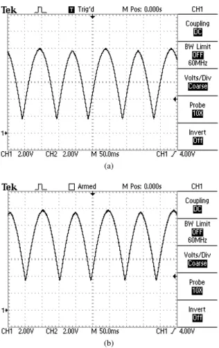
The output voltage of the PV module (VPV) is sensed using the potential divider RP and RVpv shown in Fig. 3. The output current (IPV) is measured using the sensing resistor RIpv. The voltages across RVpv and RIpv are amplified by means of the isolation and differential amplifiers with the following scale factors: VPV=3.1V/V and IPV=1A/V. The figures 4 to 8 were obtained with the digital oscilloscope Tektronix TDS210. Fig. 4 shows the output voltage of the DC/DC step-down converter (VGS shown in Fig. 3) with two different threshold voltages (minimum level). The signals shown in Fig. 4 are
suitable sweeping voltages (VGS) to control the MOSFET (a) or an IGBT (b). The minimum can vary approximately between 0 and 4 V, for different threshold voltages of power switches, and the maximum can vary between 8 and 12 V. On the contrary of what happens with a simple sinusoidal or triangular waveform, the signal used in this work is optimized for the flat region shown in Fig. 2, where the PV module behaves as a current source and the voltage VPV is sensitive to
small variations in VGS. This voltage can vary quite quickly
from Vth until the value that produces the voltage VMPP at the
output of the PV module. After that, VGS should vary more
slowly in order to increase the number of operating points captured in that flat region. As a result, the visualization of the trace of the I-V characteristics on the oscilloscope becomes moreuniform and persistent.
Fig. 5 shows the output voltage (above) and current (below) of the PV module with the sweeping voltage shown in Fig. 4(a).
The outputs VPV,isolated and IPV,isolated are fed to the inputs of the oscilloscope in the XY mode to trace the I-V characteristic of the PV module. Those outputs representing VPV and IPV are multiplied using the multiplier MPY634 in order to obtain the (a)
(b)
Fig. 4. Output voltage of the DC/DC converter (VGS) to control: (a) a
MOSFET and (b) an IGBT.
Fig. 5. Output voltage (channel 1 – 3.1V/V) and current (channel 2 – 1A/V) of the PV module.
Fig. 6. I-V characteristics of the PV module with the oscilloscope in XY mode (channel 1=X=VPV - 3.1V/V and channel 2=Y=IPV - 1A/V).
instantaneous output power of the PV module. The outputs VPV,isolated and PPV,isolated can be fed to the inputs of the oscilloscope in the XY mode to trace the P-V characteristic. Fig. 6 and Fig. 7 show respectively the I-V and P-V characteristics of the PV module EC-115.
It should be noticed that the true value of VOC is not exactly achieved because the PV module is charged with RP+RVpv, which gives a small current of 10mA when the MOSFET is OFF (open circuit). Also the true value of ISC is not exactly achieved since the PV module is not completely short circuited because of the resistance RIpv (25m ) and the internal resistance of the MOSFET (16m ).
Fig. 8 shows the I-V characteristics of the PV module when one cell (a) and two cells in parallel (b) are shadowed. The changes in the I-V characteristics are a simple example of fault diagnosis of PV modules, like the effect of partial shadowing, as in this case.
5.
Conclusions
This paper presented an improved electronic circuit for testing photovoltaic (PV) modules or strings by tracing their
I-V and P-V characteristics. A power MOSFET was used as an electronic fast varying load controlled by means of an optimized sweeping gate-source voltage, which consists of a rectified sinusoid with variable DC level for different threshold voltages.
The electronic circuit includes galvanic isolation to avoid damage of data acquisition systems and improve safety for operators, mainly in case of high voltage string tests.
Experimental results obtained with a PV module demonstrate the operation of the electronic circuit developed in this work. The I-V and P-V characteristics were monitored and captured with an oscilloscope.
The circuit can also be used for testing high voltage strings by replacing the low voltage MOSFET by a high voltage one or an IGBT and selecting a different measurement resistor. The proposed circuit is suitable to be used for analysing the influence of field conditions like temperature, irradiance and partial shadowing on the PV module performance, as well as in identifying degradation and malfunction conditions.
References
[1] IEA-PVPS, “Trends in Photovoltaic Applications”, Tech. Rep. IEA-PVPS T1-17: 2008, [Online] Available: http://www.iea-pvps.org, 2008.
[2] EPIA and Greenpeace, “Solar Generation V – 2008”, [Online] Available: http://www.epia.org, 2008.
[3] E.L. Meyer and E.E. Van Dyk, “Assessing the Reliability and Degradation of Photovoltaic Module Performance Parameters”, IEEE Transactions on Reliability, Vol. 53, N.º 1, pp. 83–92, March 2004.
[4] E.E. Van Dyk, A.R. Gxasheka, E.L. Meyer, “Monitoring Current–Voltage Characteristics and Energy Output of Silicon Photovoltaic Modules”, ELSEVIER, Renewable Energy 30, pp. 399–411, 2005.
[5] Ausias Garrigós and José Blanes, “Power MOSFET is Core of Regulated-DC Electronic Load”, EDN, pp. 92–93, March 17, 2005.
[6] Yingying Kuai, S. Yuvarajan, “An Electronic Load for Testing Photovoltaic Panels”, ELSEVIER, Journal of Power Sources 154, pp. 308–313, 2006.
[7] F. Recart, H. Mäckel, A. Cuevas and R.A. Sinton, “Simple Data Acquisition of the Current-Voltage and Illumination Voltage Curves of Solar Cells”, in Proc. 4th World Conference on Photovoltaic Energy Conversion, May 2006, Vol. 1, pp. 1215–1218.
[8] Francesco De Lia, Salvatore Castello and Luigi Abenante, “Efficiency Degradation of C-Silicon Photovoltaic Modules After 22-Year Continuous Field Exposure”, in Proc. 3rd World Conference on Photovoltaic Energy Conversion, May 2003, pp. 2105–2108.
[9] E.E. Van Dyk, A.R. Gxasheka, E.L.Meyer, “Monitoring Current–Voltage Characteristics of Photovoltaic Modules”, in Proc. 29th IEEE Photovoltaic Specialists Conference, 2002, pp. 1516–1519.
[10] Muhammad H. Rashid, Power Electronics Handbook, Academic Press, 2001.
[11] Stuart R. Wenham, Martin A. Green, Muriel E. Watt and Richard Corkish, Applied Photovoltaics, 2nd edition, Earthscan Publications, 2007.
(a)
(b)