Brazilian Journal of Physics, vol. 40, no. 3, September, 2010 357
Pentacene based Thin Film Transistors with High-k Dielectric
Nd
2O
3as a Gate Insulator
R. Sarma
Thin Film Laboratory, Department of Physics, J B College, Jorhat, Assam, India
D. Saikia
Thin Film Laboratory, Department of Physics, J B College, Jorhat, Assam, India and Dibrugarh University, Dibrugarh, Assam, India
Puja Saikia,∗ P.K.Saikia, and B.Baishya
Dibrugarh University, Dibrugarh, Assam, India (Received on 19 June, 2010)
We have investigated the pentacene based Organic Thin Film Transistors (OTFTs) with High-k Dielectric Nd2O3. Use of high dielectric constant (high-k) gate insulatorNd2O3reduces the threshold voltage and sub
threshold swing of the OTFTs. The calculated threshold voltage -2.2V and sub-threshold swing 1V/decade, current ON-OFF ratio is 1.7×10⁴and mobility is 0.13cm2/V.s. Pentacene film is deposited onNd2O3surface
using two step deposition method. Deposited pentacene film is found poly crystalline in nature.
Keywords: Pentacene, Organic Thin Film Transistors, Low Threshold voltage, Rare earth oxideNd2O3, Two Step Deposition.
1. INTRODUCTION:
Organic Thin Film Transistors(OTFTs) have received con-siderable attention from the standpoint of developing low-cost or large-area electronics applications like electronic pa-per displays, flexible sensors, and disposable radio frequency identification tags [1]. In recent years, many studies have been devoted to improving the characteristics of organic thin-film transistors (OTFTs) [2]. Pentacene organic semiconduc-tors have become one of the most promising materials for fu-ture thin, light, and flexible display applications. However, there are many problems still unresolved such as low mobil-ity, high driving voltages, etc. There have been many inves-tigations for improving mobility and other performances of OTFTs. The performance of the OTFTS can be improved by proper selection of Gate dielectric material and metal electrodes (metals which can give good ohmic contact) [3]. Most successful gate dielectric for pentacene based OTFTs is thermally grown silicon dioxide but the operating voltage of these silicon dioxide insulated OTFTs is large, above 20 V. For portable applications, especially for radio frequency identification devices requiring low power consumption, it is necessary to reduce the operating voltage to below 5 V. The key to low voltage operation is reduction of threshold volt-age and sub threshold swing. The use of a high dielectric-constant (k) gate dielectric lowering the operation voltage of TFTs is one of the main technical trends [4,5]. Therefore researchers all over the world worked on the way to reduce operating voltage of pentacene based OTFTs using various high dielectric constant insulatorsAl2O3[4],H f LaO[5,6], H f SiOx [7], Pr6O11 [8], La2O3 [9] etc. However, though the dielectric capacitance and strength of the gate dielectric are incredibly important properties, the surface characteris-tics of the gate dielectric can also play a vital role. High dielectric-constant (k) gate dielectric are characterized by a relatively rough surface morphology upon deposition in
∗Electronic address:[email protected]
a vacuum chamber. The rough surfaces result in an infe-rior channel/dielectric interface along with poor crystalline growth of the pentacene channel, and thus OTFTs fabricated on such dielectric surfaces usually exhibit undesirable device characteristics with low current ON-OFF ratio. Very thin or high-k gate dielectrics generally may bring about high leak-age current and low dielectric strength in the utilization of OTFTs.
The rare earth oxides(Nd2O3),Er2O3,Pr2O3,ZrO2etc., are reported with very high dielectric constant and low leak-age current reliable for gate dielectrics in microelectron-ics [10,11]. One of us Baishya [12] study the suitability of rare earth oxides in thin film transistors. One of the above neodymium oxide(Nd2O3)as high-kgate dielectric has been under intense investigation recently for replacing conven-tionalSiO2due to its high dielectric constant and low leak-age current. The properties of grown film and interface show a pronounced dependence upon the deposition process and the precise deposition parameters. Many techniques such as chemical vapor deposition, atomic layer deposition, sol-gel techniques, electron beam deposition etc. are used to deposit thin films on the aforementioned rare earth oxides. Each technique has their own set of advantages and disad-vantages. However, most of these techniques show some or other kind of interface damage [13]. Sputtering and e-beam assisted depositions create radiation induced surface damage during film growth. Thermal evaporation is a well known technique that does not produce any kind of surface damage [13,14]. Because this technique is a rather gentle process it creates very little or no damage to the interface [13].
Inorganic TFTs with thermally evaporated Nd2O3 ox-ide insulating layer reported successfully from this labora-tory [15,16]. Structure and Electrical Properties of Ther-mally Evaporated Nd2O3 thin films was studied by Kan-nan et al. [17,18] and reported that the thermally deposited films thickness bellow 2650 ˚Ashows well amorphous struc-ture. Amorphous dielectric films are usually insensitive to impurities and [7,19] and more stable owing to the absence of grain boundaries hence suitable for gate insulator.
semiconduc-358 R. Sarma et al.
tor layer over Nd2O3 dielectric surface. The two-step-deposition (TSD) technique, based on controlling deposi-tion rate (DR) [22,23]. This technique enables us to control the channel conductivity in the depletion and accumulation regime as well as to improve the film continuity [20,21]. The substrate temperature is kept at 270C during deposition be-cause it is found that [24] at that temperature best poly crys-talline thin films of pentacene can be grown.
The performance of the OTFT also depends on the contact electrode [25]. We have [8,9,26] already studied pentacene and tetracene based OTFTs using Al contact electrode and it is found that that best result cannot be obtained with Al-source drain electrode. As a Al-source/drain (S/D) electrode, currently, gold has been mainly used as a contact metal in pentacene based OTFTs because gold has a work function of 5.1 eV, which is close to the highest occupied molecular orbital(HOMO) level of pentacene (5.0 eV). As a result hole injection barrier is low so that carriers can move easily in each direction between electrode and pentacene. Therefore in this work we use Au as source drain contact electrode.
2. EXPERIMENTAL DETAILS
OTFTs were fabricated in staggered electrode structures by a series of vacuum evaporations using suitable masks. The order of the deposition is shown in Fig. 1. In the fabri-cation process first Al-gate electrodes of thickness 1010 ˚Ais deposited over ultrasonically cleaned (with acetone, ethanol and de-ionized water) glass substrate, above which a layer of Nd2O3of thickness 650 ˚Ais deposited. The oxide was prop-erly degassed in vacuum for a long time prior to deposition. Following the oxide layer a layer of pentacene (Aldrich of 99.9%purity), thickness 380 ˚Ais deposited using the two-step deposition method. First monolayer of 120 ˚Awas growth us-ing 0.5 ˚A/s deposition rate and the next layer of thickness 260 ˚A deposited with the rate 0.1 ˚A/s. Finally the source drain electrodes of Au (thickness 1430 ˚A) are deposited us-ing shadow mask havus-ing a channel of length 50µm and width 0.14 cm. All the depositions are done at room temperature (270C) and at a vacuum better than 5
×10−6torr using
ther-mal evaporation method. The experimental arrangement to study the electrical properties of the OTFTs is shown in fig-ure 2.
3. RESULTS AND DISCUSSION
Drain currentIDversus drain voltageVDat variousVGare
plotted in Figure 3, The graphs established that the OTFTs operate in the accumulation mode and Pentacene is p-type semiconductor. In saturation regionVD=VG−VT; drain
current is given by Eq. 1 [3]
-IDsat=
w
2Lµci(VG−VT) 2
(1)
wherewis the channel width,Lis channel length,ciis the
ca-pacitance per unit area of the gate insulator,VT is the
thresh-old voltage andµis the mobility. Plot of(IDsat)1/2versusV
Gis shown in the Figure 4. The
field effect mobilityµis calculated from the slope of this plot.
DRAIN (Au) SOURCE (Au)
Insulator (Nd2O3)
GATE (Al)
Organic Semiconductor (pentacene)
Substrate (glass)
FIG. 1: Deposition order of the OTFT.
FIG. 2: Experimental arrangement.
The threshold voltageVT is estimated by the extrapolation of
the linear portion of the graph to theVGaxis [3]. Plot of Log (ID)versusVGat a constant drain voltage(-15V) is shown in
the Figure 5. The sub-threshold swing is calculated from the
-25 -20 -15 -10 -5 0
-0.000055 -0.000050 -0.000045 -0.000040 -0.000035 -0.000030 -0.000025 -0.000020 -0.000015 -0.000010 -0.000005 0.000000
-25 -20 -15 -10 -5 0
-0.000025 -0.000020 -0.000015 -0.000010 -0.000005 0.000000
ID
in Am
p
.
VD in Volt
VG= -3V VG=-6V
VG=-9V
VG=-12V
V G=-15V
Brazilian Journal of Physics, vol. 40, no. 3, September, 2010 359
-16 -14 -12 -10 -8 -6 -4 -2 0 2 4 0.000
0.001 0.002 0.003 0.004 0.005 0.006 0.007
-16 -14 -12 -10 -8 -6 -4 -2 0 2 4
0.000 0.001 0.002 0.003 0.004 0.005 0.006 0.007
(- I
Dsat
)
1/2
in
Amp.
1/2
VG in Volt
FIG. 4: Plot of(−IDsat)1/2versusVG
-16 -14 -12 -10 -8 -6 -4 -2 0 2 1E-11
1E-10 1E-9 1E-8 1E-7 1E-6 1E-5
1E-4 -16 -14 -12 -10 -8 -6 -4 -2 0 2
1E-11 1E-10 1E-9 1E-8 1E-7 1E-6 1E-5 1E-4
VG in Volt
-ID
in Ampere
s=1V/decade
FIG. 5:Log10(ID)vs.VGplot atV D=−15V.
slope of this graph using the relation (2)
[27]-s=
δ
(logID)
δVG
−1
(2)
The current ON-OFF ratio is estimated from the relation (3) [3]
ION
IOFF
=ciµ(VG−VT)
2
σdVD (3)
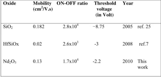
The J-V characteristics of the dielectric film in Al/Nd2O3/Au configuration is shown in the figure 6. The films shows very low leakage current and hence suitable for OTFTs. In Figure 7 the XRD pattern of the pentacene film deposited over Nd2O3 is shown. The observed diffraction peaks established that thin films of Pentacene grown over Nd2O3by two step deposition method at 270C is poly crys-talline in nature and consist of only thin film phase. The vari-ous parameters used and evaluated in this work are tabulated in table 1. In table 2 a comparative study with the previ-ous works is done. From the comparative study it is clear thatNd2O3will be better insulator for low voltage pentacene based OTFTs. Though the mobility of the OTFTs withSiO2
-10 -8 -6 -4 -2 0 2 4 6 8 10 1E-14
1E-13 1E-12 1E-11 1E-10 1E-9 1E-8 1E-7 1E-6 1E-5 1E-4 1E-3 0.01 0.1 1 10 100
-10 -8 -6 -4 -2 0 2 4 6 8 10
1E-14 1E-13 1E-12 1E-11 1E-10 1E-9 1E-8 1E-7 1E-6 1E-5 1E-4 1E-3 0.01 0.1 1 10 100
Voltage( in Volt)
Cu
rrent Density
(J) in
A/cm
2
FIG. 6:J−Vcharacteristics.
10 20 30 40 50
(003) (002)
Int
e
ns
it
y
2θ degree
(001)
FIG. 7: XRD of the pentacene film deposited onNd2O3.
insulator is a little better, the threshold voltage is consider-ably less in our case.
TABLE 1: The various parameter used and evaluated are shown in the Table bellow.
Channel width(w)
Channel length(L)
Capacitance per unit area (ci)
Channel thickness(d)
Threshold voltage(VT)
Channel Mobility(µ)
Sub threshold swing(s)
ON-OFF ratio
0.14 cm
0.005 cm
0.0016 F/m2
380A0
-2.2V
0.13 cm2/V.s
1V/decade
1.7 x10⁴
360 R. Sarma et al. TABLE 2: Comparison of present work with previous works.
Oxide Mobility ON-OFF ratio Threshold Year (cm2/V.s) voltage
(in Volt)
SiO2 0.182 2.8x10
4
−8.75 2005 ref. 25
HfSiOx 0.02 2.6x10³ -3 2008 ref.7
Nd2O3 0.13 1.7x10
4
-2.2 2010 This
work
4. CONCLUSIONS
Using two step deposition onNd2O3dielectric we fabri-cate low threshold voltage OTFTs. The threshold voltage and sub threshold swing of the OTFTs are low enough so that they can be used in portable devices. Numbers of works on
low threshold voltage OTFTs have been reported but in those works complicated fabrication techniques some times more than one fabrication technique and insulating layers are used. In this work we use traditional fabrication technique which is widely applied in commercial fabrications of TFTs, now a days. The comparative study in the table 2 established the superiority of the present work over the others. Using this method fabrication of low cost OTFT will become possible so that the traditional Si-TFTs can be replaced.
Acknowledgement
The authors R. Sarma and D. Saikia are thankful to Uni-versity Grant Commission, New Delhi, India for financial support under major research project program Grant No.: 34-20/2008 (SR). Special thanks to Google Research Help Group.
[1] Howard E. Katz and Jia Huang,Annu. Rev. Mater. Res.39,71
(2009).
[2] M.J. Malachowski and J. ˙Zmija,Opto Electron. Rev.,18(2), 121 (2010).
[3] B.C. Shekar, Jiyeon Lee and Shi-Woo Rhee,Korean J Of Che. Eng, 21(1) 267(2004).
[4] Xiao-Hong Zhang, Benoit Domercq et al.,Organic Electron-ics8, 718 (2007).
[5] M.F. Chang, P.T. Lee, S.P. McAlister, and Albert Chin,IEEE Electron Device Lett, 30(2), 133, (2009).
[6] M.F. Chang, P.T. Lee, S.P. McAlister, and Albert Chin,IEEE Electron Device Lett.29(3), 215(2008).
[7] Hu Yan, Tsubasa Kagata, Susumu Arima, Hiroshi Sato, and Hidenori Okuzaki,phys stat sol (a),205(12), 2970(2008). [8] R. Sarma, D. Saikia, and B. Barua , Organic Thin Film
Tran-sistor withPr6O11dielectric layer (pp- 42),In: Indo-Russian
Workshop on Nanotechnology and Laser Induced Plasma Pro-ceedings (IRNANO-2009).
[9] R. Sarma and D. Saikia, K. Konwar and B. Baishya ,Indian J. Phys. 84 (5), 547 (2010).
[10] Markku Leskela and Mikko Ritala, Journal of Solid State Chemistry171, 170 (2003).
[11] Markku Leskela, Kaupo Kukli and Mikko Ritala,Journal of Alloys and Compounds,418,27(2006).
[12] P. Singh, B. Baishya , physica status solidi (a), 104, 885 (1987).
[13] M. Bhaskaran, P.K. Swain and D. Misra, Electrochemical and Solid-State Letters. 7 (6), F38 (2004).
[14] R. Garg, D. Misra and P.K. Swain, J. Electrochem Soc. 153
(2), F29 (2006).
[15] P. Singh, B. BaishyaThin Solid Films, 147,25(1987). [16] P. Singh, B. Baishya Thin Solid Films, 141,179(1986). [17] M.D. Kannan, S.K. Narayandass, C. Balasubramanian and D.
Magalaraj,phys stat sol (a),128, 427(1991).
[18] M.D. Kannan, S.K. Narayandass, C. Balasubramanian and D. Magalaraj,phy stat sol (a),121,515 (1990).
[19] N.F. Mott,Adv Phy,16, 49 (1967).
[20] Sung Hun Jin, Cheon An Lee et al.,IEEE Elect. Dev. Lett.26
(12), 903(2005).
[21] Tossapol Tippo1, Chanchana Thanachayanont et al.Journal of Microscopy Society of Thailand,23(1), 130(2009)
[22] R. Ruiz, D. Choudhary, B. Nickel et al.Chem. Mater,16 (23), 4497(2004).
[23] Frank-J. Meyer zu Heringdorf, M.C. Reuter & R.M. Tromp, Nature,412, 517 (2001).
[24] C.D. Dimitrakopoulos and D.J. Mascaro ,IBM J. Res. & Dev.
45 ( 1), 11(2001).
[25] Chih-Wei Chu, Sheng-Han Li, Chieh-Wei Chen, Vishal Shrotriya, and Yang Yanga, Appl. Phys. Lett. 87, 193508 (2005)
[26] R. Sarma and D. Saikia,Indian J Pure & Appl Phys,47,876 (2009)
[27] Jung Hoon Seo, Jae-Hong et al. Semicond. Sci. Technol.22,
1039 (2007).