Fluorine-Foped Tin Oxide Substrates
*e-mail: [email protected]
Thin Copolymer-Cased Light-Emitting Display Made with
Fluorine-Foped Tin Oxide Substrates
Rudolf Lessmann, Ivo Alexandre Hümmelgen*
Group of Organic Optoeletronic Devices, Departamento de Física, Universidade Federal do Paraná, C.P. 19044, 81531-990 Curitiba - PR, Brazil
Received: December 15, 2003; Revised: May 30, 2004
Seven-segment displays are used to show numerical quantities in electronic equipment, being present in most of the low-end electronics. In this work we describe a novel organic light emitting display made with poly(1,10 – decanedioxy – 2 – methoxy 1,2 – phenylene 1,2 – ethenylene -3,6 – dimethoxy - 1,4 – phenylene - 1,2 – ethenylene – 3 – methoxy - 1,4 - phenylene) (OPPVDBC), tris(8-hydroxyquinoline)aluminum salt (Alq3) and a hole injection layer (PEDOT:PSS: poly(3,4 -ethylenedioxythiophene) : poly(styrenesulfonate)). The general device structure is FTO/ PEDOT:PSS/OPPVDBC/Ca/Al or FTO/PEDOT:PSS/OPPVDBC/Alq3/Ca/Al. The FTO (fluorine-doped tin oxide) thin films are transparent (transmittance > 80 % in the visible region of the spectrum), conductive (< 15 Ω/º for 200 nm thick films), and present high chemical stability.
Keywords:electroluminescence, copolymer, fluorine-doped tin oxide
1. Introduction
Since the development of the first organic light-emit-ting diode (OLED) with low drive voltage and high electroluminescence1, organic electroluminescent devices
presented a great evolution in structure. In spite of this evo-lution ITO (indium-tin oxide) continues to be largely used, even with the known constraint of indium diffusion into the organic layers2-5.
It was observed that the use of TO (tin oxide) instead of ITO, as transparent electrode, reduces the photolumines-cence suppression of PPV converted from a polyelectrolyte precursor6, suggesting higher chemical stability of the TO
electrode. OLEDs were demonstrated using TO as trans-parent electrode7-9, but the lower work function and the
higher electrical resistivity of TO, when compared to ITO, inhibited a wider use of TO in OLEDs. Fluorine-doped tin oxide (FTO) has transparency comparable to that of ITO and can now be produced with sheet resistance similar to that of ITO, being much more stable from the chemical point of view. Intermediate layers like PEDOT:PSS, poly(3,4 -ethylenedioxythiophene): poly(styrenesulfonate), or sulfonated polianiline can be used to effectively reduce the potential barrier for positive charge carrier injection10,11, so
that the low work function of FTO does not more constitute
a serious problem limiting FTO use in organic device ap-plications.
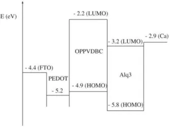
In this work we use a complex, but well-established con-cept of device structure, using FTO as anode, instead of ITO. As the hole injecting layer we used PEDOT-PSS (Baytron P®) (poly(3,4 - ethylenedioxythiophene) : poly(styrenesulfonate)), and OPPVDBC (poly(1,10 – decanedioxy – 2 – methoxy - 1,2 – phenylene - 1,2 – ethenylene - 3,6 – dimethoxy - 1,4 – phenylene - 1,2 – ethenylene – 3 – methoxy - 1,4 - phenylene))12,13 was used
as hole transport layer, HTL (see Fig. 1). In the organic heterolayer used in this work the recombination zone is ex-pected to be located at the interface between OPPVDBC and Alq3 [tris(8-hydroxyquinoline)aluminum salt], which was used as electron transporting layer (ETL),due to the energetic discontinuity of the relevant energy levels of the layers (HOMO: highest occupied molecular orbital; and LUMO: lowest unoccupied molecular orbital). Alq3, is still an interesting material due to its high electroluminescent efficiency.
2. Experimental
re-sistance of 15 Ω/) supplied by Flexitec Eletrônica Orgânica Ltda were cut in pieces of 23.0 × 32.5 mm2, patterned using conventional lithography and etched14. After patterning, FTO substrates were cleaned in a 1:4 solution of H2O2:H2SO4 for 1 h and rinsed in ultra-pure water and isopropanol. No change in surface morphology or transmittance spectra of the FTO was noted due to these cleaning, patterning and etching procedures. Absorbance spectra were measured us-ing an Optometrics spectrophotometer. Film thickness was determined using a Dektak3 surface profiler.
PEDOT-PSS dispersed in H2O was treated in ultrasonic bath for 10 h to dissolve undesired clusters before filtering. PEDOT-PSS was deposited onto glass/FTO by spin-coat-ing at 4.200 rpm. After deposition, the sample was dried in a vacuum oven at 313 K for 4 h. OPPVDBC was dissolved in distilled CHCl3 and deposited onto glass/FTO/PEDOT-PSS by spin-coating at 200 rpm, resulting in an OPPVDBC film thickness of ~ 45 nm. Alq3, Ca and Al, were evapo-rated in high vacuum, at 71 × 10 –6 Pa, with thickness of 45 nm, ~ 200 nm and ~ 200 nm, respectively. The fully evapo-ration sequence was done without vacuum breaking. Alq3 and metal film geometry were controlled through shadow masks geometry during evaporation.
Devices without the Alq3 layer were also made for com-parison.
After evaporation, the samples were transported in air to a glove box with dry N2 atmosphere. After 48 h under N2 flux the samples were encapsulated15,16. Electrical and opti-cal measurements were made in the dark. Emission spectra of FTO/PEDOT:PSS (50 nm)/OPPVDBC (20 nm)/ Alq3(45 nm)/Ca/Al device and of FTO/PEDOT:PSS (50 nm)/OPPVDBC (20 nm)/Al/Ca device were recorded with an OceanOptics CCD spectrophotometer with a 50 µm ap-erture optical fiber and with an Hitachi spectrofluorimeter, respectively.
The Ionization Potential (IP) was estimated using cy-clic voltammetry, correcting the oxidation onset at Ag/Ag+ quasi-reference electrode to vacuum reference level17 and the LUMO was estimated summing the energy of the opti-cal gap to the HOMO-energy18. The voltammetry was per-formed in a single compartment electrochemical cell. Gold was used as working electrode and a 0.1 mol/l LiClO4 solu-tion in acetonitrile, as electrolyte.
3. Results and Discussion
Taking the oxidation onset of the cyclic voltammogram of OPPVDBC at ~ 0.53 V and using the procedure described in17, the IP was estimated as ~ 4.9 eV, that summed to the optical gap of ~ 2.6 eV18 leads to an estimated electroaffinity of ~ 2.3 eV. Taking these values and using literature data for the other device layers (Alq319, PEDOT20, FTO21), we constructed the device energy scheme, presented in Fig. 2.
The PEDOT layer is introduced because it is able to effec-tively eliminate the potential barrier between PEDOT and the substrate10, in our case, FTO. It strongly collaborates to charge injection in this device, so that positive charge car-rier injection in the OPPVDBC layer is not inhibited by the energy barrier at the anode interface. Similarly, the intro-duction of the Alq3 layer strongly improves the negative charge carrier injection, leading to higher current density through the device, when compared to a device without Alq3 layer, as can be seen in Fig. 3. It was observed that current-voltage I(V) characteristics of both devices, FTO/
PEDOT:PSS/OPPVDBC/Alq3/Ca/Al and FTO/
PEDOT:PSS/OPPVDBC/Ca/Al, show negligible rectifica-tion.
The device without Alq3 presents lower
electroluminescent intensity, leading to a higher noise-level electroluminescent signal (Fig. 4), but could be seen under amber light conditions. More important, however, is that the introduction of the Alq3 layer implies in a significant reduction of the onset voltage for light emission, from ~ 11 V to ~ 6 V. Comparing the spectra of both de-vices, presented in Fig. 5, we observe a red shift of about 30 nm in the device with Alq3 layer, indicating that the re-combination zone in this device is preponderantly located inside the Alq3 layer22. It is important to observe that the
Figure 1. Chemical Structure of OPPVDBC; R. Lessmann et al.
Figure 2. Proposed energy band diagram of the device layers,
Fluorine-Foped Tin Oxide Substrates
optical gaps of OPPVDBC and of Alq3 are almost the same, permitting, in principle, exciton diffusion across the OPPVDBC/Alq3 interface. The calculated CIE coordinates are x = 0.29 = 0.58 for the FTO/PEDOT:PSS (50 nm)/
OPPVDBC (45 nm)/Alq3 (45 nm)/Ca Al and x = 0.22,
y = 0.37 for the FTO/PEDOT:PSS (50 nm)/OPPVDBC (20 nm)/Ca/Al device.
In the device with Alq3, the thickness of the HTL (OPPVDBC) and ETL (Alq3) is the same. It is interesting to notice that reported mobilities for negative charge carri-ers in Alq3 (µeAlq3 ~ 10-6 cm2/V.s)2 and for positive charge carriers in OPPVDBC (µhOPPVDBC ∼ 10-9 cm2/V.s)18 are quite different. In this case one would expect a displacement of
the recombination zone into the OPPVDBC layer, since the electrode interfaces are assumed to present no constraints for charge injection, permitting to assume ohmic injection. Under these conditions it results that radiative recombina-tion is much more favored in Alq3 than inOPPVDBC or that there is a net exciton flow at the OPPVDBC/Alq3 to the Alq3 layer due to a difference in exciton binding energy, which would be higher in the Alq3.
We have succeeded in turning on all display segments
Figure 3. J × V characteristics of a FTO/PEDOT:PSS (50 nm)/
OPPVDBC (20 nm)/Ca/Al device (circles) and a FTO/PEDOT:PSS
(50 nm)/OPPVDBC (45 nm)/Alq3 (45 nm)/Ca/Al device (squares);
R. Lessmann et al.
Figure 4. Electroluminescent intensity (EL) as a function of bias
voltage (V) of a FTO/PEDOT:PSS (50 nm)/OPPVDBC (20 nm)/ Ca/Al device (circles) and of a FTO/PEDOT:PSS (50 nm)/
OPPVDBC (45 nm)/Alq3 (45 nm)/Ca/Al device (squares); R.
Lessmann et al.
Figure 5. Electroluminescence (EL) spectrum of FTO/PEDOT:PSS
(50 nm)/OPPVDBC (20 nm)/Alq3(45 nm)/Ca/Al device at 8.5 V
(noise filtered). Circles: Electroluminescence spectrum of FTO/ PEDOT:PSS (50 nm)/OPPVDBC (20 nm)/Al/Ca device at 13 V;
R. Lessmann et al.
Figure 6. Photograph of two encapsulated 7 segments displays,
made of FTO/PEDOT:PSS/OPPVDBC/Alq3/Ca/Al, the left one
having all segments on, each one driven by a constant current of
of a seven-segment display. Segments till 16 mm2 were made showing good uniformity (Fig. 6). We made FTO rails wide enough to avoid enhanced resistivity problems. The display was connected to an electronic circuit to count numbers and worked well with the LEDs operating at ~ 8 V, demonstrat-ing that FTO is suitable for use in LEDs with large active areas and consequently, long conducting paths.
Another point that deserves discussion concerns the work function of FTO and its consequences to device operation. In the device, the PEDOT:PSS layer was used to change the effective energy barrier for charge injection, so that it al-most effectively equals the difference d of the chemical potential of the PEDOT:PSS and the anode work function3, producing a built-in potential and an electric field in the conjugated materials layers (in our case OPPVDBC and Alq3). Considering that thermodynamical equilibrium is established equalizing the electrochemical potential of the electrodes, an additional contribution to the built-in poten-tial appears as a consequence of the difference ∆φ in elec-trodes work functions24. These two contributions result that the built-in potential equals ∆φ + δ, which is the energy difference between the work function of the cathode and the PEDOT:PSS electrochemical potential, i. e., independ-ent of the anode work function. This means that in princi-ple, in case of devices with intermediate layer like PEDOT:PSS, the anode work function would not be rel-evant for device operational characteristics. These consid-erations presume that the PEDOT layer has the capability to compensate the potential difference δ. Since this com-pensation is done by polarization and charge transfer, it re-quests a minimum thickness of the PEDOT:PSS layer, oth-erwise the integration of the electric field throughout the sample thickness can be lower than δ.
Another important aspect that must be stressed is that the substitution of the ITO anode by FTO eliminates the problem of indium diffusion into the electroluminescent polymer layer2-5 due to the absence of indium in the anode material composition.
Previous investigations on FTO used in organic LEDs showed that devices prepared onto FTO substrates presented lower turn-on-voltage for current and for light and more light for a given voltage, with one observed drawback, higher leakage currents21.In the referred study, however, no inter-mediate layer was used to improve charge injection from the FTO and device performance was dependent on FTO cleaning procedure, despite the fact that the work function of FTO is not sensible to specific adopted cleaning proce-dure21, like in the case of TO6.
4. Conclusions
We have demonstrated that large seven-segment displays can be constructed using low sheet resistance fluorine-doped
tin-oxide as anode material. To demonstrate it we constructed FTO/PEDOT:PSS/OPPVDBC/Alq3/Ca/Al devices in a ge-ometry useful for low-end electronics.
Acknowledgements
The authors thanks to CAPES and CNPq for financial support, Winston S. L. Fung for the motivation and Flexitec Eletrônica Orgânica Ltda for providing the FTO substrates. We want to thank Dr. D. Ma who provided OPPVDBC ma-terial.
References
1. Tang, C.; VanSlyke, S. Appl. Phys. Lett. v. 51, p. 913-915, 1987.
2. Schlatmann, A.R.; Wilms Floet, D.; Hilberer, A.; Garten, F.; Smulders, P.J.M.; Klapwijk, T.M.; Hadziioannou, G. Appl. Phys. Lett. v. 69, p. 1764-1766, 1996.
3. Chao, C.I.; Ru, K.; Chen, S. A. Appl. Phys. Lett. v. 69, p. 2894-2896, 1996.
4. Herold, M.; Gmeiner, J.; Drummer, C.; Schwoerer, M. J. Mater. Sci. v. 32, p. 5709-5719, 1997.
5. de Jong., M.P.; van Ijzendoorn, L.J.; de Voigt, M.J.A.; Appl. Phys. Lett. v. 77, p. 2255-2257, 2000.
6. Arias, A.C.; Roman, L.S.; Kugler, T.; Toniolo, R.; Meruvia, M.S.; Hümmelgen, I.A. Thin Solid Films v. 371, p. 201-206, 2000.
7. Hümmelgen, I.A.; Yadava, Y.P.; Roman, L.S.; Arias, A.C.; Fernandes, M.R.; Nart, F. C.; Bull. Mater. Sci. v. 19, p. 423-427, 1996.
8. Arias, A.C.; de Lima, J.R.; Hümmelgen, I.A. Adv. Mater. v. 10, p. 392-394, 1998.
9. Vaufrey, D.; Ben Khalifa M.; Besland, M.P.; Sandu, C.; Blanchin, M.G.; Teodorescu, V.; Roger, J.A.; Tardy, J. Synth. Met. v. 127, p. 207-211, 2002.
10. Roman, L.S.; Berggren, M.; Inganäs, O. Appl Phys Lett v. 75, p. 3557-3559, 1999.
11. Roman, L.S.; Mello, R.M.Q.; Cunha, F.; Hümmelgen, I. A.; J. Solid State Electrochem. v. 8, p. 118-121, 2004. 12. Yang, Z.; Hu, B.; Karasz, F. Macromolecules v. 28,
p. 6151-6154, 1995.
13. Jiang, X.; Liu, Y.; Song, X.; Zhu, D. Solid State Commun. v. 99, p. 183-187, 1996.
14. Bradshaw, G.; Hughes, A. J. Thin Solid Films v. 33, L5-L7, 1976.
15. Toniolo, R.; Hümmelgen, I.A. Brazilian Patent Appli-cation, PI0201050-0.
16. Toniolo, R.; Hümmelgen, I.A. Macromol. Mater. Eng., accepted for publication. v. 289, p. 311-314, 2004 17. Micaroni, L.; Nart, F.C.; Hümmelgen, I.A. J. Solid State
Electrochem. v. 7, p. 55-59, 2002.
Fluorine-Foped Tin Oxide Substrates
19. Ohmori, Y.; Fuji, A.; Uchida, M.; Morishima, C.; Yoshino, K. Appl. Phys. Lett. v. 63, p. 1871-1873, 1993. 20. Cacialli, F.; Kim, J. S.; Brown, T. M.; Morgado, J.; Granström, M.; Friend, R. H.; Gigli, G.; Cingolani, R.; Favaretto, L.; Barbarella, G.; Daik, R.; Feast, W.J. Synth. Met. v. 109, p. 7-11, 2000.
21. Anderson, A.; Johansson, N.; Bröms, P.; Yu, N.; Lipo, D.; Salaneck, W. R. Adv. Mater. v. 10, p. 859-863, 1998.
22. Kim, K.; Lee, D.; Jin, J. Synth. Met., v. 114, p. 49-46 2000.
23. Kepler, R.; Beeson, P.; Jacobs, S.; Anderson, R.; Sinclair, M.; Valencia, V. Appl. Phys. Lett. v. 69, p. 3618-3620 1995.