Development of a Dynamically
Extensible SpiNNaker Chip Computing
Module
Rui Emanuel Gonçalves Calado Araújo
Master in Electrical and Computers Engineering Supervisor: Jörg Conradt
Co-Supervisor: Diamantino Freitas
O projeto SpiNNaker desenvolveu uma arquitetura que é capaz de criar um sistema com mais de um milhão de núcleos, com o objetivo de simular mais de um bilhão de neurónios em tempo real biológico. O núcleo deste sistema é o "chip" SpiNNaker, um multiprocessador System-on-Chip com um elevado nível de interligação entre as suas unidades de processamento. Apesar de ser uma plataforma de computação com muito potencial, até para aplicações genéricas, atualmente é ape-nas disponibilizada em configurações fixas e requer uma estação de trabalho, como uma máquina tipo "desktop" ou "laptop" conectada através de uma conexão Ethernet, para a sua inicialização e receber o programa e os dados a processar.
No sentido de tirar proveito das capacidades do "chip" SpiNNaker noutras áreas, como por exemplo, na área da robótica, nomeadamente no caso de robots voadores ou de tamanho pequeno, uma nova solução de hardware com software configurável tem de ser projetada de forma a poder selecionar granularmente a quantidade do poder de processamento. Estas novas capacidades per-mitem que a arquitetura SpiNNaker possa ser utilizada em mais aplicações para além daquelas para que foi originalmente projetada.
Esta dissertação apresenta um módulo de computação dinamicamente extensível baseado em "chips" SpiNNaker com a finalidade de ultrapassar as limitações supracitadas das máquinas SpiN-Naker atualmente disponíveis. Esta solução consiste numa única placa com um microcontrolador, que emula um "chip" SpiNNaker com uma ligação Ethernet, acessível através de uma porta série e com um "chip" SpiNNaker. Além disso, um programa de computador multi-plataforma baseado em Java disfarça esta solução personalizada permitindo que este novo sistema seja retrocompatível com todas as ferramentas existentes para as máquinas convencionais.
Para desenvolver esta nova solução foi necessário um estudo profundo e detalhado da ar-quitetura e do funcionamento interno do "chip" SpiNNaker. Com o conhecimento adquirido a partir desta análise aprofundada, foi possível construir uma placa com um microcontrolador e um "chip" SpiNNaker conectados através dum protocolo interno da arquitetura SpiNNaker. Após a criação da placa, desenvolveu-se o software para controlar o microcontrolador e uma aplicação para manter a retrocompatibilidade com sistemas padrão. Para demonstrar as novas capacidades desta plataforma noutras aplicações para além de redes neuronais, desenvolveu-se uma simulação do movimento dum bando de pássaros.
A solução apresentada permite a utilização de dezenas de núcleos ARM eficientes num pacote de reduzida dimensão, sendo desta forma adequada para ser utilizada em pequenos robots e assim implementar algoritmos avançados que exijam poder computacional paralelo.
The SpiNNaker project has created an architecture that is capable of scaling up to a system with more than a million embedded cores in order to simulate more than one billion spiking neurons in biological real time. The heart of this system is the SpiNNaker chip, a Multi-Processor System-on-Chip with a high level of interconnectivity between its processing units. Although it is a very powerful computing platform, even for non-neural application, it is currently only available in fixed configurations and it requires a workstation, usually a desktop or a laptop connected through an Ethernet connection, to be initialised and to receive the data to be processed.
Therefore if one wishes to take advantage of the capabilities of the SpiNNaker chip in other fields, as for example the robotics field specially in the case of small or flying robots, a new hardware solution with custom software must be built where the amount of processing power can be granularly selected. This new capability allows the SpiNNaker architecture to be used in more applications than it was originally designed for.
This thesis presents a Dynamically Extensible SpiNNaker Chip Computing Module to improve on the limitations of the currently available SpiNNaker machines. This approach is a single board with a microcontroller which emulates an Ethernet connected SpiNNaker chip accessible through a serial port and a single SpiNNaker chip placed together. Additionally it features a cross-platform Java based computer program that disguises this custom solution allowing this new system to be backwards compatible with all the existing tools for the standard machines.
In order to develop this new solution, a very deep and detailed study of the inner workings of the SpiNNaker chip was required. With the acquired knowledge from this thorough analysis, it was then possible to build a custom board with a microcontroller and the SpiNNaker connected through a internal protocol from the SpiNNaker architecture and develop the software to drive the microcontroller and an application to emulate a standard system for the SpiNNaker tools. A non-neural application, the simulation of the movement of a flock of birds, was developed to demonstrate the general purpose capabilities that this new platform has.
The presented solution allows the deployment of dozens of power efficient ARM cores avail-able in a very small package suitavail-able to be used in small robots which makes it possible to imple-ment advanced algorithms that require truly parallel computational power.
I wish to thank, first and foremost, to Professor Jörg Conradt who continuously supported and encouraged me, besides the technical advice essential for the development of this work. I am also thankful to my co-supervisor Professor Diamantino Freitas for his availability, support and criticism. Besides my supervisors, I would like to thank Nicolai Waniek and Christian Denk for their precious suggestions and feedback.
This thesis would not have been possible without the precious help from Steve Temple, Luis Plana and Francesco Gallupi from the University of Manchester who provided essential guidance while studying the SpiNNaker system.
I thank my fellow student, Tobias Brennich, whose help in the assembly of the multiple testing and final boards proved to be invaluable.
I owe my deepest gratitude to my family, especially my parents, Rui and Manuela, and my siblings, Mónica, Beatriz and Francisco, for their unconditional love and support.
I reserve a special thank you, to my soul mate, Ângela Igreja for all your love, affection,encouragement, motivation, support and availability, along this path. I would also like to thank all of my friends,
especially to Ricardo Castro, for all their encouragement and support .
Rui Araújo
Carl Schoonover
1 Introduction 1 1.1 Context . . . 1 1.2 Motivation . . . 2 1.3 Goals . . . 2 1.4 Methodology . . . 3 1.5 Main Results . . . 4 1.6 Related Works . . . 4 1.7 Document Structure . . . 6
2 The SpiNNaker System 7 2.1 Architecture . . . 7 2.1.1 Inter-chip communication . . . 15 2.1.2 SDP packets . . . 16 2.1.3 SpiNNaker machines . . . 22 2.2 Application Loading . . . 22 2.2.1 Boot sequence . . . 23
2.2.2 Application Load and Execute (APLX) File Format . . . 33
2.2.3 SpiNNaker Control & Monitor Program (SC&MP) . . . 36
2.2.4 SpiNNaker Application Runtime Kernel (SARK) . . . 36
2.2.5 Toolchain . . . 37
2.3 Summary . . . 39
3 SpiNNaker Chip Computing Module 41 3.1 General Architecture . . . 41 3.2 Hardware . . . 42 3.2.1 Components Selection . . . 45 3.2.2 Power Dissipation . . . 46 3.2.3 Layout Concerns . . . 47 3.2.4 PCB Test Board . . . 47 3.2.5 PCB Final Board . . . 48
3.2.6 SpiNNaker Extension Board . . . 48
3.3 Microcontroller Firmware . . . 48 3.3.1 M0 Core . . . 50 3.3.2 M4 Core . . . 54 3.4 Workstation Application . . . 57 3.4.1 User Interface . . . 60 3.4.2 Wrapper Protocol . . . 60 3.5 Evaluation . . . 62 ix
3.6 Summary . . . 63 4 Case Study 65 4.1 Boids Model . . . 65 4.2 General architecture . . . 66 4.2.1 SpiNNaker implementation . . . 66 4.2.2 Computer Visualiser . . . 68 4.3 Evaluation . . . 69 4.4 Summary . . . 69
5 Conclusions and Future Work 71 5.1 Summary . . . 71
5.2 Difficulties . . . 72
5.3 Future Work . . . 72
5.3.1 PCB Layout . . . 72
5.3.2 Full Workstation Independence . . . 72
A Developed Hardware 73 A.1 Test Board . . . 73
A.2 Final Board . . . 73
A.3 SpiNNaker Extension Board . . . 73
B SDP over P2P Packets 89 B.1 Payload of the different packets used . . . 89
C Source code 93 C.1 Microcontroller Firmware . . . 93
C.2 Workstation application . . . 93
C.3 Boids Simulation . . . 93
D SARK Source code and API 95 D.1 SARK API . . . 95
1.1 Work Methodology: phases and respective research methods . . . 4
2.1 Block diagram of the SpiNNaker chip. . . 8
2.2 Block diagram of the ARM928 core. . . 10
2.3 Emergency routing. . . 11
2.4 The 4 different SpiNNaker Packets. . . 13
2.5 SpiNNaker Communications model. . . 17
2.6 SDP packet header. . . 18
2.7 SDP packet embedded within a UDP packet. . . 19
2.8 SDP over P2P protocol. . . 20
2.9 SCP packet. . . 21
2.10 102 Machine. . . 23
2.11 103 Machine. . . 24
2.12 SpiNNaker Machines. . . 25
2.13 Node-Boot process until the selection of the Monitor processor. . . 27
2.12 Node-Boot process after the selection of the Monitor processor. . . 28
2.13 State machine for the reception of the System-Boot image. . . 30
2.14 Packet scheme used by the Host System to push the second stage image to a SpiN-Naker chip. . . 31
2.15 Packet scheme used by the SpiNNaker chip to push the second stage image to a neighbour chip. . . 32
2.16 Word array for a Flood-Fill Block. . . 33
2.17 Typical APLX file structure. . . 34
2.18 SpiNNaker programming framework. . . 38
2.19 SpiNNaker neural networks simulation development route. . . 40
3.1 General Architecture of the developed solution. . . 42
3.2 Possible connection between the microcontroller and the SpiNNaker chip. . . 43
3.3 AutoBGA user interface for the parameter configuration. . . 44
3.4 PCB Test Board. . . 48
3.5 The SpiNNaker Computing Module. . . 49
3.6 Microcontroller Firmware Architecture. . . 50
3.7 Packet Input Reading Algorithm. . . 52
3.6 Packet Input Reading Algorithm. . . 53
3.7 Host communication task state machine. . . 55
3.8 SDP Packet Transmission State Machine. . . 57
3.9 SDP Packet Reception State Machine. . . 58
3.10 SpiNNaker Wrapper Application Architecture. . . 59
3.11 User Interface of the Workstation Application. . . 61
4.1 Architecture for the Boids simulation. . . 67
4.2 A frame of the Boids Visualiser with 2176 birds. . . 70
A.1 Schematic of the initial testing board. . . 75
A.2 Developed PCB layout for the initial testing board. . . 77
A.3 SpiNNaker 102 machine with the test board. . . 79
A.4 Schematic of the final design. . . 81
A.5 Final PCB layout with the SpiNNaker chip and power supplies. . . 83
A.6 Schematic of the SpiNNaker extension board. . . 85
A.7 SpiNNaker chip extension board. . . 87
2.1 Multicast Output Vector Assignment. . . 14
2.2 P2P Table Entry behavior. . . 14
2.3 2-of-7 Symbol coding. . . 16
2.4 IPTag timeout values. . . 18
2.5 Timeout values for SDP over P2P. . . 19
2.6 Retries count for SDP over P2P. . . 21
2.7 5 SCP commands that both SC&MP and SARK implement. . . 21
2.8 Ordered list of power-on self-tests performed during Node-Boot. . . 25
2.9 APLX header and APLX Command structure . . . 35
2.10 Event Callbacks Arguments. . . 37
3.1 Power dissipation for the various regulators. . . 47
3.2 Commands send by the Application to the Microcontroller . . . 61
3.3 Commands send by the Microcontroller to the Application . . . 62
3.4 Performance Measurements for the transmission and reception of SpiNNaker pack-ets. . . 63
4.1 Frames per second for the simulation with and without the SpiNNaker Computing Module. . . 69
API Application Programmable Interface
APLX Application Load and Execute
APT Advanced Processor Technologies
ASCII American Standard Code for Information Interchange
BGA Ball Grid Array
BSD Berkeley Software Distribution
CCR Cyclic redundancy check
CPU Central Processing Unit
DDR Double Data Rate
DMA Direct Memory Access
DMIPS Dhrystone Millions Instructions per Second
DTCM Data Tightly-Coupled Memory
EAGLE Easily Applicable Graphical Layout Editor
EDA Electronic Design Automation
ELF Executable and Linkable Format
EEPROM Electrically Erasable Programmable Read-Only Memory
FIQ Fast Interrupt Request
FLOPS Floating-point Operations Per Second
FPGA Field Programmable Gate Array
FPS Frames Per Second
FR Fixed Route
GALS Globally Asynchronous Locally Synchronous
GPIO General Purpose Input Output
GPL General Public License
IRQ Interrupt Request
JAR Java Archive
LED Light-emitting diode
IPC Interprocessor Communication
ITCM Instruction Tightly-Coupled Memory
MAC Media Access Control
MC Multicast
MIPS Millions Instructions per Second
MPSoC Multi-Processor System-on-Chip
NN Nearest-neighbour
NoC Network on Chip
NRZ Non-Return-To-Zero
OSI Open Systems Interconnection
P2P Point to Point
PCB Printed Circuit Board
RAM Random Access Memory
ROM Read Only Memory
RTZ Return To Zero
SARK SpiNNaker Application Runtime Kernel
SATA Serial Advanced Technology Attachment
SCP SpiNNaker Command Protocol
SC&MP SpiNNaker Control & Monitor Program
SDP SpiNNaker Datagram Protocol
SDRAM Synchronous dynamic random access memory
SoC System on Chip
SpiNNaker SPIKING Neural Network Architecture
SRAM Static Random Access Memory
TCAM Ternary Content-addressable Memory
UDP User Datagram Protocol
VIC Vector Interrupt Controller
Introduction
The inner workings of the biological brain is still one of the great challenges for computational neuroscience despite an increasing amount of experimental data and deeper scientific understand-ing of individual components such as neurons.
There is a general consensus that the human brain has roughly about 85 to 100 billion neurons
total [Ngu10] where each neuron can have up to 15000 connections to other neurons via synapses
[Bro09]. Using techniques such as magnetic resonance imaging it is possible to observe large-scale brain activity. However, this knowledge is insufficient to truly understand how thoughts are constructed and how information is generally processed. It is believed that these functions
probably lie in the intermediate levels of the brain [FB09]. In order to understand these middle
layers, it is necessary to construct very large systems of spiking neurons with structures inspired by the latest findings from the neuroscience field.
General purpose digital architectures are not well suited to simulate these kinds of networks since these networks are characterized by massive processing parallelism and a high level of in-terconnectivity between the processing units. A possible approach is the usage of neuromorphic
systems such as the BrainScales [PGJ+12] or the Neuro-grid [CSF+12] which emulate the neural
network with a physical implementation of the individuals neurons. Another possible approach is a massively-parallel computer architecture with a high bandwidth inter-process communication
like the SpiNNaker system [FB09].
1.1
Context
The SpiNNaker system is a massively-parallel computer architecture based on a Multi-Processor System-on-Chip (MPSoC) technology that can scale up to a million cores and is capable of simu-lating up to a billion spiking neurons in biological real time with realistic levels of interconnectivity between the neurons.
The SpiNNaker system was designed under the latest paradigm for high-performance com-puting, highly-parallel systems. However, it is motivated by the attempt to understand and study biological computing structures which achieve high level of parallelism with frugal amounts of
energy as opposed to traditional electronics designs which up until the last few years were mostly driven by the serial throughput. The biological approach to the design of this many-cores ar-chitecture also brings new concerns in terms of fault-tolerance computation and efficiency. The SpiNNaker chip, the basic building block of a SPiNNaker machine, relies on smaller processors than other machines but in greater number, it has 18 highly efficient embedded ARM processors
that allows the SpiNNaker system to be competitive according to two metrics, MIPS/mm2 and
MIPS/W.
1.2
Motivation
The currently available machines with SpiNNaker chips are relatively large, the minimum size at this moment is 105 × 95mm, which limits their deployment on systems with limited size as for example, small mobile robots, specially flying ones due to very strict weight and space constraints. Additionally the SpiNNaker systems currently require a workstation, usually a desktop or a laptop, connected through an Ethernet connection to bootstrap the system every time it powers on and to feed the processing data into the system. This requirement seriously limits the independence and deployment capabilities of systems with embedded SpiNNaker chips. At present, it is necessary to
add an wireless router in order to have a mobile system with a SpiNNaker machine [DLBG+13].
The drawbacks from this approach are fairly obvious, such as increased power consumption and space requirements since the typical wireless router consumes around 4 to 5 Watt and even though there are fairly small models available at the market it would still take up some space.
Furthermore the amount of extensibility provided by standard SpiNNaker machines is very limited since it only allows increases of computing power in fixed amounts. The current single board SpiNNaker machines are available in two versions, one with four chips and another with forty eight. These are wildly different amounts of processing capability which make it difficult to create intermediate solutions. It would be interesting to have the capability of selecting how many SpiNNaker chips one needs to deploy without having to design new hardware.
The current requirements of the SpiNNaker architecture are not suitable for a lot of applica-tions where its processing power and capabilities would be helpful. It is then necessary to design a new solution that can overcome the limitations of the present options.
1.3
Goals
This thesis focused on the detailed study of the SpiNNaker architecture, with special care given to the analysis of the inner workings of the SpiNNaker chips during its bootstrapping procedures and its communications protocols with other chips in the system. The main objective from this study is the identification of the most relevant limitations and possible paths to overcome these.
The primary goal of this research is to bring this advanced and efficient computing platform to new ventures with increased flexibility. Having identified the main flaws and possible solutions to overcome them, the most significant requirements can be determined. These are as follows:
• Small size – in order for this system to be available for deployment in as many fields as possible, it must have reduced dimensions or allow for significant reductions in size with future iterations. This requirement makes it feasible to include this new computing platform in many more applications;
• Extensible – the basic solution should have only one SpiNNaker chip but it must allow the system to be extended in order to be a compelling option for applications that require greater amounts of computing power;
• Low cost – it should strive to use low cost components and only the ones required for the solution;
• Backwards Compatibility – the new solution must be compatible with tools and frame-works that are currently available for the SpiNNaker machines. The requirement increases the value of the new solution by allowing previous developments based on standard SpiN-Naker machines to be used on the new system with minimal or no work required.
1.4
Methodology
The methodology devised for this research to reach the defined goals includes the following
phases, as depicted in Figure1.1.
1. Information Gathering: The initial phase of the research was dedicated to gather and synthesize information on the SpiNNaker system and specially on the detailed behaviour of the SpiNNaker chip and on its communication with other chips. The results of this research
are presented in chapter2.
2. Development Approach:
The solution development was done in stages. The initial step was the design of a basic hardware version in order to allow the start the development of the software while still iterating on the final hardware design. The second stage was the continued improvement of the software up until the point it could boot SpiNNaker system by itself. The final step was the competition of the software to be feature complete in terms of the various capabilities that the communication subsystem of the SpiNNaker system has. This style of development led to successive improvements on the previous layers when new features or changes of functionality were required.
3. Evaluation Approach:
In order to do a validation of the developed solution, besides the standard test-bench mea-surements, a case study of a computation-intensive process with special random
characteris-tics was built. The simulation of the movement of a flock of birds [Rey87] was implemented
may bring. This example was tested on the developed solution as well as on a standard SpiNNaker machine to validate the backwards compatibility requirement.
Figure 1.1: Work Methodology: phases and respective research methods
1.5
Main Results
The main contribution of the research is a new high performance computing module based on the SpiNNaker chip which is small and cost efficient to be used on mobile platforms such as small robots. The main features of the developed module are:
• Small size – Removing the Ethernet jack among other non-essential components allowed significant reductions in total size of the new board even though the current proof of concept is a only one sided. It features also a single SpiNNaker chip and a microcontroller that emulates an Ehternet connected SpiNNaker chip.
• Extensible – The developed board has a 34 pin connector that allows the system to be augmented with other SpiNNaker machines or a custom single SpiNNaker board.
• Backwards Compatibility – A computer application written in Java was developed that allowed the system to masquerade as a standard SpiNNaker machine, capturing the UDP datagram used by the standard tools.
Another contribution from the developed work during this thesis, is the detailed study
pre-sented in chapter2on the innards of the SpiNNaker architecture. It is a collection of the
knowl-edge present in the several articles and documents available from the researchers who created this biological inspired computing platform.
1.6
Related Works
The SpiNNaker system, although biological inspired and designed to help the study of the be-haviour of large neural network of spiking neurons, is still a fairly general purpose architecture
since it makes use of small ARM embedded cores which are general purposes processors. There is an alternative named neuromorphic system which are a class of devices that implements
par-ticular features of biological neural networks in their physical circuit layout [CSBR10]. One of
these type of systems has been designed by the BrainScaleS project, a universal neuromorphic
computing substrate [PGJ+12], whose central component is the neuromorphic microchip Spikey.
This microchip contains analog very-large-scale integration (VLSI) circuits that model the electric behaviour of neurons and synapses. In this type of modelling, measurable quantities in the circuit
have biological equivalents as for instance, the membrane potential Vm of a neuron is modelled
by the voltage over a capacitor Cm. On Spikey, the standard leaky integrate-and-fire (LIF) neuron
model with conductance-based synapses, depicted in equation1.1, is implemented.
Cm
dVM
dt = −g1(Vm− E1) −
∑
i gi(Vm− Ei) (1.1)This neuromorphic system includes a Field Programmable Gate Array (FPGA) to interface the system with a Host computer that is responsible for generating configuration data as well as input stimuli to the network. It was not possible to find the power consumption of this system but depending on the selected FPGA it should be lower than the comparable SpiNNaker system since the power consumption of neuromorphic chips is much lower than equivalent digital designs
[ID00].
Another neuromorphic system, although this one is a multi-chip solution, is the Neurogird
[CSF+12] which is capable of simulating a million neurons connected by billions of synapses
in real-time. It has sixteen 12 × 14mm Neurocores where the layers of the neural networks are mapped and SRAMs and a FPGA to relay the packets with the spikes. The power consumption for the entire system is 3.1W which is a very low number for the number of neurons emulated. For comparison purposes, a comparable SpiNNaker system would consume 90W.
The biggest advantage from the neuromorphic systems is the low power consumption specially when compared to regular digital circuits. On the other hand, these systems are very tailored to the original models they were designed for and although they have some reconfigurability, it is still very limited when compared with a more general purpose approach like the SpiNNaker architecture.
There are other general purposes solutions which have designed as massively parallel
high-performance computing, as for instance, the IBM BlueGene/Q Compute Chip [HOF+12] which is
the basic unit of computing for the Blue Gene Project [GBC+05] which is an IBM project aimed at
designing supercomputers that can reach operating speeds in the petaFLOPS (for FLoating-point Operations Per Second) range, with low power consumption. This is the third design generation after BlueGene/L and BlueGene/P. The compute chip design shares some designs decision with the SpiNNaker chip. It features 18 processing units, with one used as spare and another in charge
of management tasks, although the cores used are a variant from the PowerPC A2 [IBM12]
down-clocked to 1.6 GHzfrom the original 2.3 GHz design speed as opposed to the embedded ARM cores used in the SpiNNaker architecture. Nevertheless, the main objective of this chip is to have
maximum throughput, as opposed to the SpiNNaker design where the design guidelines lead to some performance sacrifice for increased efficiency. The rated power consumption for the Blue-Gene/Q Compute Chip is 55 W while delivering a peak performance of 204.8 gigaFLOPS. It was not possible to find a Dhrystone performance measurement for this chip in order to compare it with the SpiNNaker architecture which achieves 1.1 DMIPS/MHz.
1.7
Document Structure
This dissertation is organized in four more chapters, besides the current one.
Chapter2 describes the SpiNNaker chip in detail, starting by the hardware perspective and
later analysing the several layers of software that are needed on a standard SpiNNaker machine.
Chapter3presents the developed solution, the SpiNNaker Chip Computing Module while the
chapter4describes the evaluation.
Lastly, chapter 5reviews the dissertation as a whole, explains results and points questions for
future research, that might improve the proposed solution. Appendix Adisplays the developed
hardware, with the schematics and the PCB layouts for all the developed boards, and appendix
B has a detailed diagram with the format of the packets used in a SpiNNaker specific protocol.
AppendixChas some details on the code organization and on its availability and appendixDhas
The SpiNNaker System
The SpiNNaker chip is the basic building block of the SpiNNaker system. This system was designed with the aim of simulating up to a billion spiking neurons in (biological) real-time
[NLMA+09]. This system is intended to serve as the brain of mobile robots to provide
real-time stimulus-response behaviour [ES03] and to help improve the understanding of the brain
ar-chitecture. The system was biologically inspired which allowed it to take advantage of several characteristics such as the lack of memory coherence and the slow pace of biological neurons when compared to artificial ones together with regular neuron losses. In fact, the average human
adult loses about a neuron per second without any visible consequences [FB09] meaning that the
SpiNNaker machine must be resilient to failures, since the sheer scale of the project will lead to frequent problems from which the system must recover and work around without the need for manual intervention.
This chapter presents the SpiNNaker in detail since it is a state-of-art biologically inspired system that it is not available for sale to the general public.
2.1
Architecture
The SpiNNaker machine has massively parallel architecture which can hold up to 65536 nodes, where each node is a SpiNNaker chip, a System on Chip (SoC) device with 18 low power ARM968 processors and a common 128 M byte SDRAM. One of the most important guidelines while the SoC was designed was low energy consumption since it was assumed that the cost of processors can be considered negligible when compared to the cost of the energy for the duration of the system lifetime. These guidelines explain the use of efficient embedded ARM9 cores and Mobile DDR ( Double Data Rate ) SDRAM where some performance was sacrificed in exchange of for lower power consumption. For inter-chip communications, self-timed channels were used which require much less power than synchronous links of the same capacity although they are more costly in wiring.
(Input) Comms NoC (Output) Comms NoC Proc3... 2of7 Enc 2of7 Dec 2of7 Dec 2of7 Dec 2of7 Dec 2of7 Dec 2of7 Dec 2of7 Enc 2of7 Enc 2of7 Enc 2of7 Enc 2of7 Enc
EvenClk EvenClk OddClk EvenClk OddClk
Proc0 Proc1 Proc2 Proc15 Proc16
System NoC MemClk JTAG Debug 10MHz Router control Decode
Packet Routing Output Engine Select OddClk PL340 SDRAM I/F Ctlr System Watch− dog RAM System ROM System Ethernet Ether MII 1Gbit DDR SDRAM I/O Port Reset Test Proc17 POR APB Slave AHB Master EvenClk AHB Slave OddClk RtrClk SysClk AHB Slave AXI Master AXI Master Packet Router AHB Slave Clock PLL AHB Slave AHB Slave System AHB AXI Master AXI Master AXI Master AXI Master CommCtlr CommCtlr
CommCtlr CommCtlr CommCtlr CommCtlr
Input Links Output Links RtrClk MemClk AXI Slave AHB Slave
Figure 2.1: Block diagram of the SpiNNaker chip [Gro11b].
The chip itself is a Globally Asynchronous Locally Synchronous (GALS) system with the mentioned 18 low power ARM968 processors nodes connected through an energy-efficient packet-switched asynchronous communications infrastructure. Initial SoC designs used an interconnect
paradigm based on a shared bus design [FB05]. However this paradigm is not conveniently
up-scalable when the complexity of the system increases. In order to solve this problem, SoC design-ers use a complex hierarchy of buses which allows concurrent communication with the different components partitioned in separate buses. These buses are connected through complex protocols and multiple bridges between them. This increased complexity makes it harder to meet the timing
requirements. A solution to this problem is the use of packet-switched networks [DT01] which
of-fer greater flexibility in the topology of the SoC, reduced latency and increased bandwidth through the use of additional area. Networks on Chip (NoC) decouple the timing domains of each block which simplifies the timing closure process. The SpiNNaker chip uses CHAIN, a solution devel-oped at the University of Manchester, which uses self-timed circuits with delay insensitive data
encoding combined with a return-to-zero signalling protocol to implement the packet switching
network [BF02]. Self-timed circuits ( asynchronous ) are an alternative circuit design which uses
acknowledgement to explicitly indicate and validate the data as opposed to synchronous circuits where there is a global clock to indicate the moments of data stability. There are a number of
dif-ferent designs in how to signal data validity, CHAIN uses a delay-insensitive style [Ver88] where
the data validity is transmitted implicitly in the data encoding which removes the need for much of the timing analysis since this design operates correctly regardless of the delays involved in the interconnected wires.
Figure 2.1 illustrates the main functional components. The shaded areas indicate the
asyn-chronous interconnect areas. It is clear that each chip has two NoC. The Communications NoC is responsible for transmitting packets between on-chip and off-chip processors while the System NoC replaces the traditional system bus by providing access to an off-chip DDR SDRAM, which is usually available in the same package mounted on top of the SpiNNaker die and stitch-bonded to it, and to other system control peripherals like the Router’s configuration registers, the System Controller and the Watchdog Timer.
One of the most important components is the ARM928 core which is the main processing
resource of the SpiNNaker system and whose block diagram can be seen in Figure 2.2. The
ARM698E-S is the smallest, lowest power consuming ARM9 family processor [ARM13]. Each
core in the SpiNNaker chip was configured to have 32 Kbyte of instruction tightly-coupled mem-ory ( ITCM ) and 64 Kbyte of data tightly-coupled memmem-ory (DTCM) available. It also has a timer which is used by the kernel to provide time sensitive services, a DMA controller to be used for transfers with the attached SDRAM and to communicate with the system bus, and a Communica-tions Controller. The CommunicaCommunica-tions Controller is the peripheral that allow each core to access the packet switching network present in the SpiNNaker system.
All 18 processors nodes are identical which is the cause of problems during the start-up pro-cedures. One of the processors is chosen as the Monitor Processor through a process which will be described later and it will be responsible for booting the chip, the communication with the Host PC and performing the necessary system management tasks. The other processors are named Ap-plication Processors and they will be responsible for modelling a group of neurons with associated inputs and outputs, named neuron fascicle, in neural application since the processor are general purpose in essence. Some Application processors may not be used to serve as spares for fault-tolerance purposes. The Monitor processor runs a different kernel, named SpiNNaker Control & Monitor Program (SC&MP), from the Application cores which run the SpiNNaker Application Runtime Kernel (SARK). The Monitor processor is also given access to SystemRAM which is an extra block of 32 Kbyte of on-chip RAM accessible through the System NoC. This memory is not exclusive to the Monitor processor although the latter is its main user to improve its data resources as it will be responsible for the management of the chip and run complex algorithms.
The Router is the hearth of the Communications NoC, taking up 10% of the chip’s area
[NLMA+09], as it is responsible for the routing of packets between on-chip processors and with
32KB ITCM DTCM 64KB CpuClk (~200MHz) Clock Buf/Gen AXIClk DMAClk AHBClk ARMClk CCClk Timer / Counter Controller Interrupt Communications Controller ARM968E−S AHB−Lite M Controller System NoC Comms NoC CHAIN Gateway DMA AHB M AHB S AHB S AHB2 AHB S IRQ TClk ARM IRQ/FIQ ARMClk AHBClk AXIClk DMAClk CCClk AXI Master JTAG AHB1 AHBClk AHBClk AHBClk
Figure 2.2: Block diagram of the ARM928 core [Gro11b].
through the two most significant bits in the header, the different packet formats are showed in the
diagram2.4. All packets have a 32 bit optional payload whose presence is indicated through bit 1
in the header control byte. The least significant bit indicates if the entire packet has odd parity. For almost all packet types, there is a two bit time stamp present in the control byte. This time stamp is set to the current time phase of the system. There is a global time phase that cycles through 00 -> 01 -> 10 -> 11 -> 00, synchronization should be accurate to within one time phase, which is pro-grammable and dynamically variable. If the Router finds a packet to be two time phases old, easily checked through an XOR operation, then it will drop it to the Monitor Processor. The Router is the one responsible for inserting this time stamp on local packets during normal operation though this behaviour can be overridden through configuration on the Communications Controller.
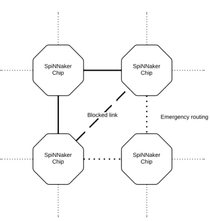
Emergency Routing
Each chip has six bidirectional links to communicate with other chips. These are numbered from 0 to 5. The recommended connection configuration is a triangular mesh where each chip is con-nected to six different neighbours. This allows for easy emergency routing in the event of a failing or congested link, the traffic that would be using the congested link is redirected using two
Figure 2.3: Emergency routing.
dependencies between links there are potential deadlock scenarios for which there is a policy in place to prevent them which is "no Router can ever be prevented from issuing its output". In or-der to enforce this policy, the Router has several mechanisms available, the output has sufficient buffering and capacity detection so that the Router can know whether or not the output can accept another packet. If an output is blocked for any reason then emergency routing is used if possible to avoid overloading the blocked output. In cases where the emergency routing fails the packet is "dropped" to a Router error register and the Monitor Processor notified of this failure. The Monitor Process will then track the problem using a diagnostic counter:
• if the problem was temporary, it will only note it but do nothing further;
• if emergency routing keeps being used for the same route, it will negotiate a new one and divert some traffic to the new link;
• if the problem is permanent, it will establish new routes for all the traffic using this link. The time taken by the Router to try emergency routing is controllable through its control register, there are two wait values, wait1 is the number of clock cycles that Router waits before trying emergency routing and wait2 which is the number of cycles that the Router tries to do route the packet through another link before dropping it to the error register and continuing to the next one. There are 2 bits in the control byte which are used by Multicast and Fixed-route packets to control the emergency routing process. The meaning of each value is as follows:
• 00 - normal packet;
• 01 - the packet has been redirected by the previous Router through an emergency route along with a normal copy of the packet, the receiving Router should treat this as a combined normal plus emergency packet, meaning it will be routed in two different ways;
• 10 - the packet has been redirected by the previous Router through an emergency route which would not be used for a normal packet;
• 11 - this emergency packet is reverting to its normal route.
Multicast Packets ( MC )
Multicast packets carry neural event information to be used during model simulations. Each packet contains an identifier which is used as a routing key as well as a neuron identifier in neural
ap-plications [PBF+08]. The multicast router behaves like a look-up table with two components, a
parallel ternary content-addressable memory (TCAM) and a conventional RAM look-up table. A content-addressable memory is a special kind of memory whose input in a read operation is the data and the output is the address where the data is located as opposed to a read from RAM where the input is a memory location and the output the data stored at that address, the ternary variation
include support for a do not care bit [PS06]. The router’s TCAM has 1024 entries, which must
be initialized after reset, each with its own mask and match value. The routing process uses the routing key present in the packet as input for the TCAM, then the TCAM result is used to retrieve from the look-up table the output vector whose value determines where this packet should be sent. In case of multiple matches from the TCAM look-up, the one with the lowest value will be used.
The table 2.1shows how each bit of the output vector, when set to 1, affects the propagation of
the multicast packet. When the routing key has no matches then the default routing is employed. The default routing simply outputs the packet on the opposite link of the input link through where it was received. For local packets this routing is not available meaning that if the packet fails to match an entry it will be dropped.
When an output link is blocked, the Router will try to do emergency routing through a link with the next lower number. If the original port becomes unblocked before sending the packet through the emergency port, then the router will retry through the original one. If the Router receives a packet with the emergency packet bits set as diverted, then it will attempt to output it as a reverting packet to the output link with the next lower number than the input link number, where it was received. If it is also a normal packet then it will also perform the conventional routing. A received reverting packet is routed normally if it is recognised by the router, otherwise it is default routed to the link numbered two greater than the input link.
Point to Point Packets ( P2P )
Point-to-point packets carry system management and control information. They are also used to implement a higher level packet transmission which it will be described later. These packets
control routing key
8 bits 32 bits 32 bits
Multicast Packet
0
optional payload
0 emergency routing time stamp payload parity 6
7 5 4 3 2 1 0
Control Byte
control
8 bits 16 bits 32 bits
Point to Point Packet
0
optional payload
1 sequence code time stamp payload parity 6 7 5 4 3 2 1 0 Control Byte source ID destination ID 16 bits control address/operation
8 bits 32 bits 32 bits
Nearest-Neighbour Packet
1
optional payload
0 debug route payload parity
6
7 5 4 3 2 1 0
Control Byte
control payload
8 bits 32 bits 32 bits
Fixed-Route Packet
1
optional payload
1 emergency routing time stamp payload parity 6
7 5 4 3 2 1 0
Control Byte
Multicast Output Vector Entry Output port Direction bit[0] Tx0 East bit[1] Tx1 North-East bit[2] Tx2 North bit[3] Tx3 West bit[4] Tx4 South-West bit[5] Tx5 South
bit[6] Processor 0 Local
bit[7] Processor 1 Local
bit[8] Processor 2 Local
... ... ...
bit[23] Processor 17 Local
Table 2.1: Multicast Output Vector Assignment [Gro11b].
include a source and destination ID, each one with 16 bits. The destination ID is used to determine which output should the packet be routed to. For each ID, there is a three bit entry which is decoded to determine whether the packet should be delivered to the Monitor Processor, sent through one
of the output links or dropped. The table2.2show the routing behaviour for each possible entry
value. These values are packet in a 8K x 24 bit SRAM lookup table sequentially. The use of a Static Random Access Memory helps reducing the access time and power consumption while
using the lookup table [YIK87]. The sequence code field present in the control byte is under
software control and can be used for any purpose.
Nearest-neighbour Packets ( NN )
Nearest-neighbour packets are used during boot-time to do flood-fill of the boot image ( to be described later ), broadcast of P2P addresses and for chip debugging. The routing process delivers
normal NN packets to the Monitor processor when receiving through one of the six input links
and it send through the appropriate output link the internally generated packets. This routing is essential to support the flood-fill load process.
When the debug bit in the header control byte is set, the NN packet is interpreted as a peek/poke
P2P Table Entry Output Port Direction
000 Tx0 East 001 Tx1 North-East 010 Tx2 North 011 Tx3 West 100 Tx4 South-West 101 Tx5 South
110 none (drop packet) none
111 Monitor Processor Local
packet which can be used by neighbouring chips to access System NoC resources without proces-sor intervention which means it can be used to investigate a non-functional chip, to re-assign the Monitor Processor or to generally debug and test easily a SpiNNaker chip. The nature of the oper-ation depends on the presence of a payload, meaning that a write operoper-ation will include a payload while the read operation will not. The address/operation field contains the address, within the Sys-tem NoC address space, where the operation will be performed, either the payload will be written to this location or the current contents will be read into the response packet. There is always a response which is a normal NN packet with the same address field for identification purposes with the least significant bit set to indicate a response. In case of bus error while accessing then bit 1 will also be set. The response will also include a payload when replying to a peek packet.
Fixed-route Packets ( FR )
Fixed-route packets usually convey application debug data back to the host computer which facili-tates monitoring and debugging. Its routing procedure is identical to the multicast packet although since they do not include routing key, the value of a specific Router’s register, in this case regis-ter 33, is used as its routing key. As a consequence, all fixed route packets are routed using the same output vector. When an output is blocked, the router will use the same emergency routing procedures that it uses for the multicast packet emergency routing.
2.1.1 Inter-chip communication
The on-chip interconnect employs a 3-of-6 return-to-zero (RTZ) self-timed codes and the
switch-ing fabric based on CHAIN [FB09]. Each inter-chip link is based on the 2-of-7 non-return-to-zero
(NRZ) self-timed coding, where each unidirectional link consists of 7 data wires and an acknowl-edge signal. The data symbols are sent using transition signalling from the Sender to the Receiver where a transition on 2 of the data wires translate to a 4 bit symbol. The sender waits for a tran-sition on the acknowledge signal to proceed to the next symbol. The logic levels 0 and 1 are represented by voltages of 0 and 1.8V respectively. After the chip reset, the output data wires are brought to logic 0 while the acknowledge goes to logic 1.
There were mainly two motivations to have two different protocols involved in the communi-cations:
• Performance; • Power consumption.
A RTZ protocol will always have two transitions on each line during a symbol transmission as opposed to a NRZ protocol which only needs one, this translate on easily doubling the through-put. As far as power consumption is concerned, minimizing transitions is essential to maximize efficiency. In this particular case, the 3-of-6 RTZ employs 8 transitions to send 4 bits of data, the 2-of-7 NRZ uses only 3 transitions to send the same data. in the off-chip domain these improve-ments are essential as chip-to-chip delays dominate performance and wire transitions dominate
Value L[6] L[5] L[4] L[3] L[2] L[1] L[0] 0 0 0 1 0 0 0 1 1 0 0 1 0 0 1 0 2 0 0 1 0 1 0 0 3 0 0 1 1 0 0 0 4 0 1 0 0 0 0 1 5 0 1 0 0 0 1 0 6 0 1 0 0 1 0 0 7 0 1 0 1 0 0 0 8 1 0 0 0 0 0 1 9 1 0 0 0 1 1 0 10 1 0 0 1 0 0 0 11 1 0 1 0 0 0 0 12 0 0 0 0 0 1 1 13 0 0 0 0 1 1 0 14 0 0 0 1 1 0 0 15 0 0 0 1 0 0 1 EOP 1 1 0 0 0 0 0
Table 2.3: 2-of-7 Symbol coding [Tem12].
power consumption, The 2-of-7 protocol offers the double of performance with less than half en-ergy consumption. These advantages do not apply in the on-chip domain as the simpler logic required to implement the 3-of-6 protocol dominates the decision on both power and performance. One common issue that self-timed codes suffer from is the lack of resistance to transient or permanent faults. The SpiNNaker inter-chip links have been designed to improve on this weak-ness by reducing the risk of deadlock as much as possible since preventing data corruption is not possible. Additionally, the SpiNNaker chip has the ability to reset sub-circuits in order to simplify recoveries from deadlocked situations.
2-of-7 Symbol coding
There are 17 different symbols where one is EoP which means End of Packet and the others are
values between 0 and 15. The table2.3shows the encoded symbol for each set of transitions, on
this table the value 1 on the data wire should be read as transitions while 0 as no transition.
2.1.2 SDP packets
The figure2.5illustrates the different layers of the SpiNNaker communications model, the Open
Systems Interconnection (OSI) model was added to show the relative function of each layer as it is a common abstraction. At this point, the bottom two layer have already been discussed. This section will analyse the third layer which builds upon the lower layers.
The basis of all communication from the host system with the SpiNNaker system is done using SpiNNaker Datagram Protocol ( SDP ) packets. The protocol is similar to User Datagram Protocol (UDP) since it is sent in datagrams and it has very few capabilities embedded in the protocol itself
Presentation Layer Session Layer Transport Layer Application Layer
Network Layer Data Link Layer
Physical Layer
Application Layer
On-chip: 3-of-6 RTZ protocol Off-chip: 2-of-7 NRZ Protocol
SpiNNaker Packets SpiNNaker Datagram Protocol
OSI Model SpiNNaker Comms Model
Figure 2.5: SpiNNaker Communications model.
besides the transmission of a limited amount of data. The SDP datagram may contain up to 64 kilobytes though the current implementation in the SpiNNaker kernel limits this value to 272 bytes in order to minimize the size of the buffers required.
A SDP packet contains a header with information needed for its routing and a payload field with the data that is being sent. Since SDP provides point to point communication, an addressing
scheme is needed to identify the endpoints. As it can be seen in Figure2.6, for each endpoint there
are 3 fields with each taking 1 byte. Two fields, "Addr X" and "Addr Y" , are used to identify the chip’s position inside a SpiNNaker system shaped into a 2D grid. The third byte is divided in two fields where the lower 5 bits are the Virtual CPU number which is unique within a SpiNNaker chip and the 3 high bits are a port number which attaches the packet to a particular process on that CPU. The convention which is in place states that port 0 is reserved for communication with the kernel running on the core and the rest of the ports are available for applications. There are two more fields in the header that must be mentioned, the Flags field which should be set to 0x87 or 0x07 if a reply is expected or not, and Tag field which holds the IPTag.
An IPTag is a small number that is used by the SpiNNaker node connected to the Ethernet port to know where to send each output SDP packet bound to the Ethernet port. This SpiNNaker node maintains a mapping between the IPTag and the IP address/port pair. Each IPTag can be permanent or transient, permanent tags are set through commands which will later be described, transient tags are created when a new SDP packet arrives for which a reply is expected. The newly created tag is then written to the packet header before delivering it to its destination. As soon as
CPU Dest Addr Y Srce Addr Y Srce Addr X X Dest Addr CPU Srce Dest Tag Flags Srce Port Dest Port 8 3 5 3 5 8 8 8 8 8 bits
Figure 2.6: SDP packet header [Tem11c].
reply reaches the Ethernet-attached node, the tag is used to retrieve the IP address needed for its routing and the IPTag table entry is deleted at this point. A transient tag can have a associated timeout that in case the reply fails to arrive the table entry can be reclaimed. The current IPTag table implementation in the SpiNNaker kernel has 16 entries where the first 4 are reserved for permanent tags.
Regarding the Virtual CPU number, each core on a SpiNNaker chip has a physical CPU num-ber which is hardwired from 0 to 17. During the boot up process, a processor is selected as Monitor processor and is assigned the Virtual CPU number 0 and the rest of Application processors from the number 1 upwards from which non-working CPUs are excluded.
SDP packets can be conveyed in a number of manners, for example, when sent from the host
system to a SpiNNaker system they are embedded within a UDP packet as seen in Figure2.7. The
2 byte pad present at the beginning of the UDP data aligns the data to a 4 byte boundary which makes the processing in a SpiNNaker rather easier. The first of the these two bytes is an argument which is used as the IPTag timeout. The valid values for this timeout go from 0 to 16 whose
meaning can be checked in table2.4.
SDP over P2P
While the SDP packets are usually introduced into a SpiNNaker system through the Ethernet port, they are transmitted between SpiNNaker chips using P2P packets. This protocol is undocumented
and it was reverse engineered from the kernel source-code. The Figure2.8shows a typical protocol
run with no errors or retries. The initial step is a request from the sender to open a channel for reception. The receptor will reply with an open acknowledgement packet with the channel id or with an error code in case either the SDP packet is too large (over 280 bytes ) or there are no free channels. Having received a normal acknowledgement packet, the sender will send sets of 16 data packets, each with 24 bits of data. At end of this set, the receptor will send a data
Value Meaning 0 No timeout ( infinite ) 1 10 ms 2 20 ms ... ... N 10 ∗ 2N−1ms ... ... 16 327680 ms
MAC
Hdr IP UDP PAD SDP SDP DATA FCS
4 8 8 2 20 (typ) Hdr Hdr Hdr SDP Packet UDP Data 14 bytes
Figure 2.7: SDP packet embedded within a UDP packet [Tem11c].
acknowledgement packet which allows the sender to send the next set of data packets. This cycle continues until the receptor has all the data packets it needs. At this point, the receptor will send a close request packet to the sender to which it should reply with a close acknowledgement packet. Then both ends close the connection. The detailed packet format for each step and their content is
presented in the appendixB.
Since this connection can be made between any two SpiNNaker chips in the system, there is fairly big timeout for each step of the protocol. Additionally, in case of errors or timeout there are also retries mechanisms for most steps of the protocol. The specific values being used in the
current implementation are presented in the table2.5and2.6.
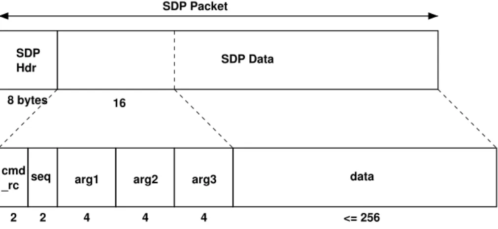
SpiNNaker Command Protocol (SCP)
One of the uses for SDP packets is to convey commands and responses around a SpiNNaker system. In this case, the SDP data field is structured into 6 fields which are shown in the Figure
2.9. The cmd_rc field indicates either the command that is being specified or the return code of
a command execution when the packet is a response. The seq field may be used to create a retry mechanism on top of SDP. The fields arg1, arg2 and arg3 may contain 32-bit arguments or return values while the data data field may contain any kind of data up to 256 bytes.
SDP packets with SCP commands should be sent to port 0 so that the kernel running at the core can process them. There are five commands which are currently implemented by both kernels.
Their names and actions can be seen in Table2.7, the reader interested in higher levels of detail
should refer to [Tem11d].
Protocol Step Timeout value ( ms)
Waiting for Open ACK packet 250
Waiting for Data ACK packet 3000
Waiting for a Data packet 500
Waiting for a Close ACK packet 250
Sender
Requests a stream to be open for the data
Acknowledges the Open Request
Sends 24 bits Sends 24 bits
Sends 24 bits
Acknowledges the data received
16 times unless the SDP packet length is smaller
than 48 bytes
Sends 24 bits Sends 24 bits
Sends 24 bits
Sends a Close request This cycle
repeats as long as there is data
to send
Acknowledges the Close request
Receptor
Initial connection procedures
When all the data has been received, the Receptor ask the Sender
to close the connection Note: In case all data is sent during the first 48 bytes, the Receptor will send a Close request
immediately.
Protocol Step Retries Count
Retries for Open requests 16
Retries for starting data transmission 4
Retries for resuming data transmission 4
Retries for Close requests 4
Table 2.6: Retries count for SDP over P2P.
SDP Hdr
16
2 2 4 4 4
cmd
_rc seq arg1 arg2 arg3 8 bytes
data SDP Packet
SDP Data
<= 256
Figure 2.9: SCP packet [Tem11d].
Command Name Action
CMD_VER Retrieves the version of the kernel
CMD_READ Allows the reading of memory from the core’s address space up to
256 bytes. The read operation can be requested in byte, halfwords and words.
CMD_WRITE The equivalent of CMD_READ for writing operations
CMD_RUN Low level command which instructs the core to start executing at
a specific address, it is not usually used.
CMD_APLX The usual way of starting an application. This instructs the kernel
to process an APLX file, which must have been loaded to memory (using CMD_WRITE) beforehand.
2.1.3 SpiNNaker machines
The Advanced Processor Technologies Research Group (APT), that has developed the SpiNNaker system, has also developed several SpiNNaker machines, each with different number of SpiN-Naker chips. Their names are formatted as 10N where N is an integer number which tells the
user that the machine has approximately 10Ncores. The 102 and 103 machines are single printed
circuit board (PCB), larger machines are cabinets and/or racks of the 103 machine [Gro13].
102 machine
The 102 machines is a 4 node board with 72 ARM cores, with 64 usually deployed as Application cores, 4 Monitor processor and 4 spares cores. It is the smallest SpiNNaker machine currently available measuring 105 × 95mm and weighting around 50 grams. It has two connectors that expose the SpiNNaker’s inter-chip link interface and a 100Mbps Ethernet standard plug, RJ-45.
This machines requires a 5V 1A supply and it is depicted in Figure2.10.
103 machine
The 103 machine has 48 nodes, which leads to 864 ARM processors. From this total, 48 are used as Monitors processors and 48 as spares processors which leaves 768 cores to be used as application cores. There are six 3.1Gbps high-speed serial interfaces, which use SATA cables though not necessarily a SATA protocol. These interfaces are used to build the larger machines, but they can also be used as general purpose high-speed input/output communications by configuring the
on-board FPGAs. These machines require a 12V 6A supply and it is depicted in Figure2.11.
104, 105 and 106 machine
The larger machines are increasingly bigger sets of 103 machine linked together through the SATA
links available on those boards. Figure 2.12 depicts the amount of cores available with each
machine, their relative sizes and their power consumption.
2.2
Application Loading
Besides the Node-Boot described below, a SpiNNaker system has no non-volatile storage from where it can load the software that will be running, so a host machine, usually a desktop or laptop, is needed. The connection between the host and the SpiNNaker is usually done with an Ethernet cable since every SpiNNaker chip has an Ethernet controller hardware on-board, though a direct connection is only possible when this is connected to an external transceiver responsible for con-necting the link layer to the physical layer of the OSI model,hereafter many times addressed as PHYceiver, and a SerialROM chip with a valid IP and MAC address.
Figure 2.10: 102 Machine [Gro13].
2.2.1 Boot sequence
There are 3 stages on the SpiNNaker booting sequence:
• The Node-Boot phase which executes the code from a read-only on-chip memory, BootROM. This code was designed to be as simple as possible to minimize the probability of bugs since it is not possible to correct them after production. It is also responsible for the initial chip testing and initialisation, the election of a Monitor Processor and having the node ready to receive the second stage image.
• The System-Boot phase where a boot image is received on the Ethernet connected SpiN-Naker node and is propagated to its neighbours until every Monitor Processor in the system is running the second stage image. This propagation of the boot image through the system
Figure 2.11: 103 Machine [Fur13].
is known as flood-fill. Following this, every working core in each chip is assigned a Virtual CPU number as described above.
• The final stage is the Application-Load where the application software is loaded from the host machine to the chosen cores, the application data uploaded to the shared SDRAM and the route tables populated.
Node-Boot
This is the first phase of the boot and the one where the initial checks are performed to check on the status of the memories and the peripherals, any failures at this stage will lead to the shutdown
of the core as may be seen in Table2.8. The very first step of the boot sequence is to check using
the external General Purpose Input/Output (GPIO) pin 7 whether a manufacturing test should be run or if the default BootROM should be executed. Assuming the latter, the cause of the boot is probed at the Register 12 of the System Controller.
If the reset was caused by the Watchdog then it is detected if an ITCM Validation Block (IVB) has been set up to detect whether the instruction memory is intact and has not been corrupted by
103 machine: 864 cores, 1 PCB, 75W 104 machine:10,368 cores, 1 rack, 900W (NB 12 PCBs for operation without aircon) 105 machine: 103,680 cores, 1 cabinet, 9kW
106 machine: 1M cores, 10 cabinets, 90kW
Figure 2.12: SpiNNaker Machines [Fur13].
Peripheral Method Executing Core Failure response
At Power-on
ITCM RAM test All Shutdown Core
DTCM RAM test All Shutdown Core
After Scatter loading
Comms controller Register test All Shutdown Core
DMA controller Register test All Shutdown Core
Timer Register test All Shutdown Core
VIC Register test All Shutdown Core
After Monitor election
Previous Monitor Check Register All Shutdown Core
SystemRAM RAM test Monitor Shutdown MP Core
Router Register test Monitor Shutdown MP Core
Watchdog Register test Monitor Shutdown MP Core
PL340 Register test Monitor Record, continue
SDRAM RAM test Monitor Record, continue
Exceptions
Exception Hi Vectors All Shutdown Core
Exception Low Vectors All Shutdown Core
any software malfunction, and to resume execution immediately. This capability is useful in cases when the simulation is already running in the system. In this case the rest of the chips would not have code to restore the reset node and the routing paths would be interrupted. The fault may have been only a glitch or a transient fault which could mean that all the operating environment may yet be in memory. The IVB is a series of checksums that allows the node to be sure that its instruction memory was intact to start executing right away, otherwise it would proceed through with the normal boot.
If it was a non-watchdog reset, as for example a power on reset, then one processor is chosen as Boot processor through external GPIO pins. This core checks for the presence of an external SerialROM chip which usually provides the MAC and IP addressing information though it may be optionally be used to exit the Node-Boot sequence early by loading and executing an image hosted in this chip. After this point, all core clocks are boosted to 160 MHz to accelerate the boot sequence since up until this point all the clocks were running at 10 MHz.
In order to initialize other peripherals, a Monitor processor must be elected first. The election is performed by a hardware mutex in the System Controller implemented as a read sensitive register. The first processor that reads back the register is selected as a Monitor. The cause of the reset is again important, if it was a soft-reset, caused by the watchdog or an intervention triggered due to an unexpected failure, it could have been caused by an error within the Monitor processor so if this core was a Monitor before it will shut itself down so that other cores may be elected, otherwise the history of Monitor Processors is cleared so that every core has a chance to be elected. The newly selected processor marks itself in the bit-wise "Monitor History" System RAM location which will be used in the soft-reset scenarios. Other processors will then become Application processors and will wait for the Monitor to finish the remaining initialization procedures.
At this stage the remaining peripherals to be initialized are the Router, the Watchdog, the Ethernet and the GPIO pins. The router tables are populated with blank entries meaning that the P2P packets will be dropped and it will only transmit multicast packets with the default routing. The Watchdog is set to expire every 1.25 seconds and the chip will reset after the second timeout of the watchdog timer. This should not happen during normal operation as it should be refreshed every 5 ms. For the Ethernet to work, an external PHYceiver must be provided and a SerialROM with the IP and MAC addresses information, it will only be initialized if both are present and functional. The last step before signalling to the Application Processors that they may continue the booting process is the initialization of some GPIO pins where there are usually some LEDs connected. These are useful to denote the stage of the boot process since the frequency of its flashes is different on every stage. One important thing to notice, is that the failure to initialize correctly the router or the watchdog will lead to the shut down of the Monitor processor and to the restart of the SpiNNaker chip, where a different Monitor will be chosen.
The final step before waiting for the reception of the System Boot image is the initializations of the processors’ timers and their Vector Interrupt Controller (VIC). The timer 1 is set to tick every millisecond in all cores but the VIC configuration depends on whether or not the processor is the Monitor processor. The Application processors only take action when the System Controller
N Boot or
Manufacturing test? Watchdog
Reset? Is IVB setup? GPIO Pin #7
Manufacturing Test?
GPIO Pin #6 Check Serial ROM
Get Info from SerialROM instructions / blocks of memory from SerialROM GPIO Pins #3:5
Select Boot Proc ID
Am I boot Processor? BootProc complete? IVB Recovery Success? Test ITCM Test DTCM Record Fault Code. Shutdown Core GPIO Pin #1 POST Enabled? POST Required? Test Comms Ctrl Test DMA Ctrl Test Timer Test VIC Fail Record Fault Code. Shutdown Core Fail Reset by Power-on? Success Y N N N Y Y Manufacturing Tests Boot Mnfrg N Y Y Run software validated in ITCM Y Success Mutex: Reset previous MonProc list Have I been MonProc? Record Fault Code. Shutdown Core Y Y N Mutex: Elect Monitor Processor N Am I the Monitor? I am an Application Processor N I am the Monitor Processor for the
Node Y If Returns, mark BootProc Done Start: BootROM 0xFFFF0000 Waiting N
N Test PHY GPIO Pin #6
Check Serial ROM
Am I the Monitor Processor?
Enter Main Loop
Missing/Faulty Present & OK Y I am an Application Processor I am the Monitor
Processor for the Node
GPIO Pin #1 POST Enabled?
POST Required?
System RAM Test Router Test Watchdog Test
Record Fault Code. Red LEDs.
Trigger restart of Appl Procs. Shtdwn Monitor Fail Y Success PL340 Test SDRAM Test Record any Fault Code & detected SDRAM size Initialise Router
N
IP/MAC from SerROM? Initialise PHY and
Ethernet Serial ROM
attached?
Initialise GPIO for LEDs & Watchdog Trigger continue to Application Procs
Initialise Timer & VIC – for system
controller intrrpts
Waiting
Initialise VIC – for timer, packet and Ethernet interrupts Switch to Low
Vectors, enable interrupts, set
CPU OK
Trigger Condition set N
Y
Y N
![Figure 2.1: Block diagram of the SpiNNaker chip [Gro11b].](https://thumb-eu.123doks.com/thumbv2/123dok_br/15707443.1068355/26.892.104.837.138.740/figure-block-diagram-spinnaker-chip-gro-b.webp)
![Figure 2.2: Block diagram of the ARM928 core [Gro11b].](https://thumb-eu.123doks.com/thumbv2/123dok_br/15707443.1068355/28.892.125.726.157.616/figure-block-diagram-arm-core-gro-b.webp)
![Figure 2.10: 102 Machine [Gro13].](https://thumb-eu.123doks.com/thumbv2/123dok_br/15707443.1068355/41.892.155.785.146.754/figure-machine-gro.webp)
![Figure 2.11: 103 Machine [Fur13].](https://thumb-eu.123doks.com/thumbv2/123dok_br/15707443.1068355/42.892.133.719.143.669/figure-machine-fur.webp)
![Table 2.8: Ordered list of power-on self-tests performed during Node-Boot [Gro11a].](https://thumb-eu.123doks.com/thumbv2/123dok_br/15707443.1068355/43.892.164.788.193.489/table-ordered-list-power-tests-performed-node-boot.webp)
![Figure 2.13: Node-Boot process until the choosing of the Monitor processor[Gro11a].](https://thumb-eu.123doks.com/thumbv2/123dok_br/15707443.1068355/45.892.155.785.122.1125/figure-node-boot-process-choosing-monitor-processor-gro.webp)
![Figure 2.12: Node-Boot process after the choosing of the Monitor processor[Gro11a].](https://thumb-eu.123doks.com/thumbv2/123dok_br/15707443.1068355/46.892.101.744.128.1145/figure-node-boot-process-choosing-monitor-processor-gro.webp)
![Figure 2.13: State machine for the reception of the System-Boot image [Gro11a].](https://thumb-eu.123doks.com/thumbv2/123dok_br/15707443.1068355/48.892.107.743.138.487/figure-state-machine-reception-boot-image-gro-a.webp)
