Bernardo Marques Rodrigues
Bachelor in Micro and Nanotechnology Engineering
Multilevel metallization
scheme using printing technologies for
IC fabrication using discrete
oxide TFTs
Dissertation submitted in partial fulfilment of the requirements for the degree of
Master of Science in Micro and Nanotechnology Engineering
Supervisor: Dr. Pedro Miguel Cândido Barquinha, Associate Professor, Faculty of Science and Technology, NOVA University of Lisbon Co-Supervisor: Dr. Man-Kay Law, Assistant Professor,
Faculty of Science and Technology, University of Macau
Panel:
Chairman: Prof. Dr. Rodrigo Ferrão de Paiva Martins Examiner: Prof. Dr. Luís Miguel Nunes Pereira
Jury member: Prof. Dr. Pedro Miguel Cândido Barquinha
Multilevel metallization scheme using printing technologies for IC fabrication using discrete oxide TFTs
Copyright © Bernardo Marques Rodrigues, Faculdade de Ciências e Tecnologia, Universidade Nova de Lisboa.
A Faculdade de Ciências e Tecnologia e a Universidade Nova de Lisboa têm o direito, perpétuo e sem limites geográficos, de arquivar e publicar esta dissertação através de exemplares impressos reproduzidos em papel ou de forma digital, ou por qualquer outro meio conhecido ou que venha a ser inventado, e de a divulgar através de repositórios científicos e de admitir a sua cópia e distribuição com objectivos educacionais ou de investigação, não comerciais, desde que seja dado crédito ao autor e editor.
“When everything seems to be
going against you remember
that the airplane takes of
against the wind not with it.”
i
Acknowledgements
First, I would like to thank professor Rodrigo Martins and Elvira Fortunato for the opportunity and for giving me access to work in CENIMAT|i3N and CEMOP research centres. Next a big thanks to my supervisor and co-supervisor Pedro Barquinha and Matthew Law for allowing me to develop this innovative project and for all the help, patience, advice and interesting ideas. Without them, this dissertation wouldn’t be complete. Also, I would like to send a special thanks to Cristina Gaspar for all the time and help provided in the laboratory. Her help provided me guidance through all the obstacles that I had to surpass. To Angelo Rodrigues and Ana Santa thank you for the design of the TFTs matrix and for the fabrication of those TFTs respectively.
Next, I must thank, my parents and my family for all the support and love throughout my life and especially along these last six months. Even when they couldn’t directly help in the work, they supported me just by listening and being there and that was more than I could ever ask.
Of course, I can’t forget the friends which are present in my life. Thanks for all the love, kindness and support I’m really grateful. A special mention to Mariana for the advice and fresh pair of eyes to improve some parts of this work and those times we spend together, to Andre for our philosophic conversations about life that help keep my head in the right place, to Alexandre thanks for the conversations about science and future perspectives, instead of training, that kept me motivated to do my best work possible and final special thanks to Laura for listening to my crises and dramas and for all the dances and fun that reenergized me to keep pressing on.
Finally, but definitively not the least, a very special thanks to Inês for entering my life in a very difficult time and in such short time changing it for the best. Thanks for all the support, patience, love, kindness and just being there when needed in those times that I just wanted to give up.
iii
Abstract
Despite the emergence of flexible electronics as a technology for manufacturing integrated circuits at lower costs than traditional silicon microelectronics, costly and time-consuming clean room processes are still needed to interconnect the various transistors that make up the circuits. In this context, this dissertation presents an alternative, based on printing processes of multi-layer metallic interconnections, that allow to connect thin film transistors (TFTs) in functional circuit blocks, thus bringing a significant cost reduction and great flexibility for the prototype of new circuits.
For such, a silver ink and polyvinylpyrrolidone (PVP) solution were used to form the conductive and insulating layer respectively. Using an inkjet printer, it was possible to pattern, on glass, silver lines with 100 and 50 µm width and a resistivity of 7.12 × 10⁻⁸ Ωm using 200 ºC for 30 min. PVP was deposited with a thickness of 3.5 µm to ensure insulation between conductive layers and a laser etching process was implemented to create vias between different metallization levels. Finally, the developed process was demonstrated in several digital circuit blocks based on oxide TFTs.
Keywords: Inkjet, Conductive ink, Multi-level metallization, Silver interconnections, Silver lines
v
Resumo
Apesar da emergência da eletrónica flexível como uma tecnologia para o fabrico de circuitos integrados com custos mais reduzidos que a tradicional microeletrónica de silício, são ainda necessários processos dispendiosos e morosos de sala limpa para interligar os vários transístores que constituem os circuitos. Neste contexto, apresenta-se uma alternativa baseada em processos de impressão de múltiplas camadas de pistas metálicas que permitem ligar transístores de filme fino (TFTs) em blocos de circuitos funcionais, trazendo assim uma redução significativa de custos e grande flexibilidade para o teste experimental de novos circuitos.
Para tal uma tinta de prata e uma solução de polivinilpirrolidona (PVP) foram utilizadas para formar a camada condutora e isolante respetivamente. Utilizando uma impressora por jato de tinta foi possível padronizar, sobre vidro, a prata em linhas de 100 e 50 µm com uma resistividade de 7.12 × 10⁻⁸ Ωm, utilizando 200 ºC durante 30 min. Entretanto, o PVP foi depositado com uma espessura de 3.5 µm de forma a garantir o isolamento entre camadas condutoras, sendo ainda implementado um processo de erosão por laser criando vias entre diferentes níveis de metalização. Por fim, os processos desenvolvidos foram demonstrados em vários blocos de circuitos digitais, baseados em TFTs de óxidos.
Palavras-chave: Impressora por jato de tinta, Tintas condutoras, pistas condutoras de prata, impressão de múltiplas camadas, interligações de prata
vii
List of acronyms
TFT - Thin film transistor PE - Printed electronics R2R – Roll to roll Ag - Silver Ag
DOD - Drop on demand CIJ - Continuous inkjet NP - Nanoparticle CNT - Carbon nanotube IR - Infrared
UV - Ultraviolet DPI - Drops per inch PVP - Polyvinylpyrrolidone RGB - Red, green and blue PPI - Pulses per inch DC – Direct current
ix
List of symbols
m - Meter nm - Nanometer µm - Micrometer ˚C - Degrees Celsius cm - Centimeter mm - Millimeter s - Seconds V - Volts mV - Millivolts mA - Milliampere Ωm - Ohm meter Ω - Ohmmm/s - Millimeter per second % - Percent wt% - Percentage in weight GHz - Gigahertz cP - Centipoise pL - Picoliter mL - Millilitre g - Grams
xi
Content
Acknowledgements ... i
Abstract ... iii
Resumo ... v
List of acronyms ... vii
List of symbols ... ix
List of figures ... xiii
List of tables ... xvii
Motivation and objectives ... xix
1.
Introduction ... 1
1.1
Printed electronics ... 1
1.2
Printing techniques and inkjet printing of conductive lines... 1
1.2.1 Inkjet ... 1
1.3
Sintering ... 4
2.
Methodology ... 7
2.1 Conductive layer ... 7
2.2 Insulating layer ... 8
2.3 Via formation by laser ablation ... 8
2.4 Characterization methods (morphological and electrical analysis) ... 8
2.5 Final prototype ... 9
3.
Results and discussion ... 11
3.1 Printing process ... 11
3.1.1 Inkjet printing silver lines on glass substrate ... 11
3.1.2 Deposition of PVP ... 17
3.1.3 Inkjet printing silver lines on PVP substrate ... 19
3.2 Sintering methods ... 21
xii
3.2.2 IR annealing ... 23
3.3 Electrical characterization of PVP layer ... 24
3.4 Via formation and characterization ... 25
3.5 Final prototype ... 28
4. Conclusions and future perspectives ... 33
5. References ... 35
xiii
List of figures
Figure 1.1-Effect of decreasing the drop spacing on the printed line morphology. a) has
the biggest drop spacing while d) has the lowest drop spacing.
9... 2
Figure 1.2- Cross-sectional profile of uniform lines printed at different temperatures.
5. 3
Figure 1.3-SEM images obtained with silver ink deposited on glass and sintered at
different temperatures
1... 5
Figure 2.1-Schematic of a cross-section of the final prototype, comprising a printed,
multilevel metallization scheme on a glass substrate with discrete oxide TFTs. ... 7
Figure 2.2- Inkscape pattern of conductive lines for optimization of the Ag printing
process ... 7
Figure 3.1-Effect of the resolution in the morphology of the printed Ag lines; a) to c) 50
µm lines with 750, 1000 and 1500 DPI respectively; d) to f) 100 µm lines with 750, 1000
and 1500 DPI respectively. ... 11
Figure 3.2- Effect of the printing speed in the morphology of the printed Ag lines a) to c)
50 µm lines with a printing speed of 100, 50 and 10 mm/s respectively; d) to f) 100 µm
lines with a printing speed of 100, 50 and 10 mm/s respectively. ... 12
Figure 3.3- Effect of the substrate temperature in the morphology of the printed Ag lines
a) to c) 50 µm lines with a substrate temperature of 30, 50 and 70 ºC respectively; d) to
f) 100 µm lines with a substrate temperature of 30, 50 and 70 ºC respectively ... 13
Figure 3.4- 100 µm Ag line printed with a substrate temperature of 30 ºC; a) speed of 100
mm/s and 750 DPI; b) speed of 100 mm/s and 1000 DPI; c) speed of 50 mm/s and 750
DPI; d) speed of 50 mm/s and 1000 DPI ... 14
Figure 3.5- 100 µm Ag line printed with a substrate temperature of 50 ºC; a) speed of 100
mm/s and 750 DPI; b) speed of 100 mm/s and 1000 DPI; c) speed of 50 mm/s and 750
DPI; d) speed of 50 mm/s and 1000 DPI ... 15
Figure 3.6- Time-lapse of the droplet formation under 50 % humidity environment .... 15
Figure 3.7- 50 µm line printed with a substrate temperature of 30 ºC; a) speed of 100
mm/s and 750 DPI; b) speed of 100 mm/s and 1000 DPI; c) speed of 50 mm/s and 750
DPI; d) speed of 50 mm/s and 1000 DPI ... 16
Figure 3.8- 50 µm line printed with a substrate temperature of 50 ºC; a) speed of 100
mm/s and 750 DPI; b) speed of 100 mm/s and 1000 DPI; c) speed of 50 mm/s and 750
DPI; d) speed of 50 mm/s and 1000 DPI ... 17
xiv
Figure 3.9- Profile taken at three different points of the insulating PVP layer obtained
with two different shear casting speeds; a) 1 mm/s; b) 2 mm/s ... 18
Figure 3.10- Profile taken at three different points of the insulating PVP layer obtained
with two different shear casting speeds and printed twice; a) 1 mm/s speed; b) 2 mm/s
speed ... 18
Figure 3.11- Profile taken at three different points of the insulating PVP layer deposited
twice, with the second layer deposited in the opposite direction with respect to the first
one and with two different shear casting speeds at 30 ºC; a) 1 mm/s speed; b) 2 mm/s
speed ... 19
Figure 3.12- Profile of two parallel samples of insulating PVP layer deposited twice, with
the second layer deposited in the opposite direction with respect to the first one, at 1 mm/s
shear casting speed and 30 ºC. ... 19
Figure 3.13- Ag lines printed on PVP with substrate temperature of 50 ºC, speed of 50
mm/s and 750 DPI a) 50 µm line b) 100 µm line. ... 20
Figure 3.14- 100 µm Ag lines printed on PVP with a substrate temperature of 50 ºC and
speed of 50 mm/s. ... 21
Figure 3.15- Resistivity Vs temperature plot for the different thermal sintering times; a)
100 µm lines b) 50 µm lines. ... 22
Figure 3.16- Resistivity Vs time plot for the different times (5, 10, 15 and 30 min) under
the IR lamp. ... 23
Figure 3.17- Test structure for calculating the breakdown voltage a) top view b)
cross-section view ... 24
Figure 3.18- Graphics of the electric field Vs current density of the PVP films using
thermal sintering methods; a) 180 ºC for 30 min; b) 200 ºC for 30 min. ... 24
Figure 3.19- Graphic of the electric field Vs current density of the PVP films sintered at
5 min under an IR lamp. ... 25
Figure 3.20- SEM images of the vias made by laser ablation; a) 2.5 % power and 1 %
speed; b) 3 % power and 1 % speed. ... 25
Figure 3.21- EDS mapping images of the via fabricated using 3 % power with 800 PPI at
1 % speed. ... 26
Figure 3.22- Profile of the via fabricated using 3 % power with 800 PPI at 1 % speed 27
Figure 3.23- I-V curves of the total resistance of the test structure utilized sintered at; a)
200 ºC; b) 5 min under the IR lamp. ... 28
xv
Figure 3.24- a) Mask layout of one oxide TFT for the final prototype b) one oxide TFT
fabricated in clean-room. ... 28
Figure 3.25- schematic of the cross-section of one TFT with two levels of metallization.
... 29
Figure 3.26- Silver lines printed on parylene with substrate temperature of 50 ºC, speed
of 50 mm/s and 750 DPI a) 50 µm b) 100 µm. ... 29
Figure 3.27 Silver lines printed on parylene with substrate temperature of 50 ºC, speed of
50 mm/s and 400 DPI with 3 layers; a) 50 µm b) 100 µm. ... 30
Figure 3.28- I-V curves of the silver lines printed on parylene, comparing the two
different printing conditions ... 30
Figure 3.29- Transfer curves for a) different TFTs in parallel; b) 10 discrete oxide TFTs;
c) not gates with different number of drive transistors; d) NAND gate at different VDD
values. ... 31
xvii
List of tables
Table 2.1- Summary of the different printing variables tested to achieve conductive Ag
lines ... 7
Table 3.1- Results of the effect of the DPIs in the morphology of the printed Ag lines. 11
Table 3.2- Results of the effect of the printing speed in the morphology of the printed Ag
lines. ... 12
Table 3.3- Results of the effect of the substrate temperature in the morphology of the
printed Ag lines. ... 13
Table 3.4-Electrical resistivity for the 100 µm line with the substrate temperature of 30
ºC with different speeds and DPIs ... 14
Table 3.5- Electrical resistivity for the 100 µm line with the substrate temperature of 50
ºC with different speeds and DPIs ... 15
Table 3.6- Electrical resistivity for the 50 µm line with the substrate temperature of 30 ºC
with different speeds and DPIs ... 16
Table 3.7- Electrical resistivity for the 50 µm line with the substrate temperature of 50 ºC
with different speeds and DPIs ... 17
Table 3.8- Width of Ag lines printed on PVP with substrate temperature of 50 ºC, speed
of 50 mm/s and 750 DPI. ... 20
Table 3.9- Electrical resistivity for the 100 µm line with different DPIs and number of
printed layers. ... 20
Table 3.10- Electrical resistivity of the different parallel samples for the selected sintering
condition (200 ºC for 30 min on a hot plate). ... 23
Table 3.11- Calculated value for the resistance of the via for the two sintering conditions
studied ... 27
Table 3.12- Width of the silver lines printed on parylene with substrate temperature of 50
ºC, speed of 50 mm/s and 750 DPI. ... 29
Table 3.13- Width of the silver lines printed on parylene with substrate temperature of 50
ºC, speed of 50 mm/s and 400 DPI with 3 layers ... 30
xix
Motivation and objectives
Traditionally electronic devices are mainly fabricated using a subtractive approach, that involves processes like photolithography and vacuum-based techniques. These techniques consists of multi-step processes, require specialized equipment and facilities and utilize hazardous materials, which translate to higher cost of production and time-consuming process. For this reason, it is starting to appear a need for a new approach to combat those problems and satisfy the market needs for simpler and cheaper manufacturing.1–3
This new approach is completely focused on additive processes and techniques, where the material is deposited directly on the desired spot, like inkjet printing and other types of printing techniques. Allowing the emergence of printed electronics, that in the past few decades has gained a lot of interest due to its massive flexibility and simplicity of production, for its one-step process. Many different materials and substrates can be used, giving it a wide range of possible applications compatible with industrial manufacturing. This solution allows a fast production rate with less waste, lowering its overall cost. Due to this kind of advantages the practical applications, that can arise from the use of this techniques are endless and constitute a very attractive and interesting area of investigations for this work. The consequences can be showed by the fact that the market is projected to reach $ 26.6 billion by 2022 from the current $ 14 billion in 2017 at a compound annual growth rate of 13.6 %.1–4
The purpose of this dissertation is to apply a set of low-cost, simple and rapid hybrid techniques to develop a multilevel metallization scheme useful to fabricate integrated circuits from discrete oxide thin film transistors (TFTs). The goal is to use different printing techniques to deposit, on a glass substrate containing high-performance, clean room fabricated oxide TFTs, multiple levels of conductive layers of silver (Ag) interconnections with line width as small as possible (sub-100 µm), with each level electrically insulated using printed insulating polymers.
To accomplish this goal, the following sub-objectives will be addressed:
i) Understanding the mechanisms and a first optimization of the printing process on regular glass and over the polymeric insulating layer.
ii) Optimization of the sintering process to convert the ink to conductive interconnections.
iii) Via formation through the insulator to connect the different levels of conductive layers, by laser ablation
iv) Comprehensive morphological and electrical characterization of the printing interconnections and insulating layer.
v) Final prototype fabrication and characterization comprised of several digital circuit blocks (NAND gate, a simple inverter and an inverter with 2 and 3 drive TFTs in parallel) using two levels of printed conductive layers.
1
1. Introduction
1.1 Printed electronics
Nowadays electronic components can be made using two different approaches: i) the conventional and widely used silicon-based microfabrication, that involves subtractive processes and techniques; ii) an additive process which gives rise to an area called printed electronics (PE).1,2
PE is an area of electronics that focus on fabricating devices by using material deposition techniques, like conventional printing techniques5 and in the last few years it has received enormous attention for being a potential alternative to the conventional approach.6,7 This is justified through to low-cost manufacturing with high throughput8, ease of integration, rapid prototyping2,9,10 and compatibility with flexible systems (e.g., large area-electronics and hybrid system fabrication on different substrates, organic or inorganic). This contrasts with classic microfabrication techniques, such as photolithography, laser ablation2 and vacuum-based techniques, that typically require complicated manufacturing processes with a significant number of steps, time bottlenecks in the prototyping and development stage. The disadvantages of these techniques are reflected in the downtime without any production, excessive material waste, high environmental impact and high production costs.1–4,6,10–14
This additive approach uses as building blocks conductive materials such as metal nanoparticles and nanowires, carbon nanotubes and graphene to fabricate transparent conductive films, flexible energy harvesting and storage devices, TFTs, electroluminescent device and wearable sensors, are some examples.1,7,8,15 All of these devices require some type of conductive structures and good alignment between layers, which means that highly conductive patterns with a high resolution are a critical component of PE which are sometimes hard to achieve.4,11
1.2 Printing techniques and inkjet printing of conductive lines
Printing techniques can be divided in two categories: i) Noncontact techniques or nozzle-based patterning; ii) contact-nozzle-based patterning. The noncontact techniques include inkjet printing, electrohydrodynamic (EHD) printing, aerosol jet printing and slot dye coating. Screen printing, gravure printing and flexographic printing are examples of contact techniques, that nowadays are the technique employed for mass printing.2,4,11
Contact printing techniques require the printing pads to be in contact with the substrate in order to transfer the inked patterns to the substrate. They typically use an embossed or engraved roll to transfer the ink to the substrate, the major problems being the potential damage induced to the bottom layer during printing and longer set-up times which usually translate into increased initial costs. In contrast, the non-contact techniques, don’t require a mask to deposit the ink, instead eject ink from a nozzle and the nozzle itself never gets in contact with the substrate. Therefore contaminations and wastages are minimal but nozzle clogging and unwanted ink spread are still problems to be addressed, due to the fact that a clogged nozzle prevents the ink from coming out (hindering the printing process) while unwanted ink spread limits the resolution of the technique.2,11 In general, most of these techniques benefit from the fact that the user controls where and how much material is deposited, eliminating the need for etching processes.10
1.2.1 Inkjet
Inkjet printing is a deposition technique for printing a wide range of functional materials.15 These materials in the form of colloidal dispersions are deposited through the micron-sized printing nozzle, with the advantage of being extremely accurate9 and conformal16 over large areas at a fast speed and low cost17. Additionally, small amounts of materials can be deposited (picolitre size drops in the range of 20-50 µm,11 depending on the nozzle diameter3) with minimal waste and over rigid or flexible substrates.1,3,5,8,13,18–20 Moreover, as this is a noncontact and maskless deposition technique,20,21 resulting in minimal damage to the substrate and allows for the deposition of different materials in the same substrate4,16 resulting in minimal contaminations from previous printing processes.2,13
2
There are two main mechanisms for the printing head to generate droplets: drop on demand (DOD) printing, which is the most utilized printing mechanism and it is the selected one for this work. The other mechanism is the continuous inkjet (CIJ) printing3,13,22. These systems are now robust industrial tools and are used for high-speed graphical applications.1,4,9–11
The DOD mode, in contrast to CIJ, is characterized by a smaller droplet size, efficiency of material usage and higher accuracy. 3,13,14 The droplets are ejected by a pressure pulse generated in a chamber filled with ink behind the nozzle.3,13,14,22 This pressure can be generated either by thermal pulse, a piezoelectric actuator or by an electrostatic pulse (Attachment A).2,4 In the first one the heating resistor receives the signal to start heating up and vaporise the ink to generate the vapour bubble that in turns pushes the ink out of the nozzle. In the piezoelectric mode the deformation of the piezoelectric ceramic actuator, due to an application of an electric signal, induces a pressure wave within the ink chamber to dispense the ink droplet out of the nozzle. Finally, in electrostatic mode, the electrostatic interaction, due to a potential difference between the conductive ink and an intermediate plate coupled to the substrate holder, forces the ink to be ejected from the nozzle.2,10,11,13,22
The CIJ is characterized by the fact that the nozzle is continuously ejecting ink droplets and to control the position of each droplet the printer uses electrostatic forces to deflect them to the desired position on the substrate.22 In the case of binary deflection CIJ printing, which is one of two printing modes, the droplets are either charged, which end up deflected to the gutter, or uncharged, which makes their way to the substrate. For the multi-deflection CIJ printing, individual droplets have different charges and when this droplets pass through a fixed electric field they are deflected in multiple-directions.2
One big problem with all these systems is the possibility of aggregation, that leads to clogging of the printing nozzle, being proper ink selection one way to solve this.11,20 To help the printing process the ink should have properties within the range accepted by the printer, nevertheless, the tuning of the printing parameters also helps with this. Particle size, viscosity, surface tension and density of the ink all play an important role in the droplet formation and ejection.3,4,6,18,23 In this work the use of a commercially available ink facilitates setting all these parameters in their correct range.
Another important part of inkjet printing is the interactions of the ink with the substrate. When a liquid drop impacts the substrate there will be a period when the drop shape will be controlled by fluid properties, where surface tension and contact angle play an important role, prior to solidification. Given that normally the deposition process involves more the one droplet, the spacing of those droplets and the speed at the printing head moves are important parameters to consider because this together with the ink properties are the most responsible for the pattern morphology as seen in the Figure 1.1.3,5,9,15,22
Figure 1.1-Effect of decreasing the drop spacing on the printed line morphology. a) has the biggest drop spacing while d) has the lowest drop spacing.9
3
Typically inkjet printed lines have features size of tens to hundreds of micrometres, with the limit so far being around 30 µm,22 and thickness in the range of hundreds of nanometres and from a macroscopic point of view, the type of morphology obtained will influence the electrical performance.5 To achieve low resistivity, the printed lines should be uniform with a large cross-sectional area. For that end, many facts like substrate surface energy, ambient conditions and printing parameters have some influence. Another important fact that helps the achievement of low electrical resistivity of the lines is the sintering conditions, which will be discussed in section 1.3 of this chapter.5
Since the inkjet process deals with colloidal dispersions, solvent evaporation dynamics are essential to take into account because it leads to a common effect called the coffee ring effect. This effect originates from the capillary flow induced by the different evaporation rates across the droplet.9,24 When a droplet has a pinned three-phase contact line, the excess solvent lost at the edge is replaced by solvent from the centre, leading to a radial capillary flow and a loss of cross-sectional area.4,24 This effect is highly temperature dependent in a way that the higher the temperature during printing, drying or sintering the more the solvents will evaporate, enhancing the coffee ring effect, leading to narrower widths but a deep valley starts appearing as Figure 1.2 shows.5,24
Figure 1.2- Cross-sectional profile of uniform lines printed at different temperatures.5 Is important to suppress this effect because it directly affects the morphology of the printing patterns, which in terms affects the resolution of the pattern and consequentially the performance of the device by interfering with the resistivity. There are several ways to reduce the coffee ring effect, like ink-drying on a smooth substrate or by constraining the evaporation at the edge, electrowetting or drying droplets in electric fields, a mixture of two or more liquids with different vapour pressures and surface tension or a sufficiently fast increase in viscosity after deposition.4,5
Another important effect that can happen during the printing process is the formation of internal or external cracks in the printed patterns. This can happen due to the large reductions of volume during the evaporation of the solvent, resulting in degraded electrical conductivity by introducing defects, which makes it difficult for the current to flow through the pattern.23 One way to control this effect is to select a substrate with a coefficient of thermal expansion closer to the metal in the ink.23
To achieve the best electrical performance it is useful to understand which variables affect the resistance of a printed line, as shown by the following equation:
𝜌 =𝑅 × 𝐴 𝑙
Where ρ is the material resistivity (Ωm), R is the resistance (Ω) of the line, l is the length (m) and A is the cross-sectional area (m2). From the equation, it is easily understood that the cross-sectional area needs to be maximized to ensure that the printed material’s resistivity is as close as possible to its typical bulk value. Since increasing the linewidth hinders high-density integration, increasing the thickness seems to be the most viable route, provided that transparency of the lines are not a requirement. This can be done simply by repeating the printing process several times,
4
increasing the thickness layer by layer. Nevertheless, this multi-step printing might also result in an increase of the linewidth so, in the end, the line resistance optimization has to be approached in a way that benefits the application in mind.5
Another characteristic of inkjet printing is the ink itself and the properties it should have to achieve a good printability. Conductive inks are multi-component systems containing a conducting material in a liquid medium, that can be aqueous or organic and some other additive components like rheology and surface tension modifiers, humectants, binders and defoamers, that provide a better performance of the overall system.1,20,23 The conductive material may be in the form of dispersed nanoparticles (NPs), a dissolved organometallic compound, or a conductive polymer that can be dissolved or dispersed.1,13,23 The choice of material depends on the required physical properties of what is going to be printed, such as conductivity, optical transparency, stability to bending, adhesion to the substrate, physicochemical properties of the resulting ink (like aggregation) and finally compatibility to the printer itself.1
The developed ink should have good printability, high resolution, enable minimum printer maintenance and a long shelf life, which means properties like surface tension, viscosity, wettability and adhesion to the substrate should be controlled to achieve an optimal print.1,13,18,25
Nowadays the most used material is metal NPs and the wet chemical methods used today to produce those NPs are able to meet the large scale requirements for inkjet ink formulation.1 These NPs are suspended in water or an organic solvent, such as toluene or ethylene glycol.1 The solvent chosen must quickly evaporate when deposited but not so fast that dries out at the nozzle leading to a series of problems as clogging.23 For example, silver (Ag) based metal NPs inks, which is the selected ink for this work, are the most widely used due to its high electrical conductivity and low oxidation1,5,7,8,13,18,20,25 but due to its high cost (like gold as well)5 research has been performed to find alternative material like copper or aluminium. These alternative materials are not ideal due to rapid oxidation in ambient condition, leading to an increase in the complexity of the production process in order to control the atmosphere.1,5,7,13,20,23,25
These NPs can only be used in inks if they are produced in a way that prevents them from aggregation and precipitation to ensure reproducible performance, so the addition of a stabilizing agent, like a polymeric material or a surfactant, is paramount. These stabilizers are especially important for dispersions with high metal loading (20-60 wt%) which are required to obtain printed patterns with high conductivity.1 Also, to guaranty a good printability, the NP synthesis has to be done in a way to control the size, shape and distribution of the NPs.1,13,20,23 As a general good rule of thumb the particle size should be 100 times smaller than the nozzle.20,23 Another problem with using NPs is the need for a post-printing treatment to remove this stabilizing agents and allowing the NPs to coalesce together in a sintering process (see section 1.3) resulting in conductive patterns.1,5,13,23
Is also possible to produce inks based on metal precursors dissolved in solution in the form of ions,5,13 that in this case would be silver or other metal depending on the needs of the application.5,13 Since these ions can be prevented from coagulation, the final ink can be very stable over a long time, preventing in this way the clogging of the printing nozzle.5,23The downside of this type of ink is the low metal content, which causes an increase of the electrical resistivity and also the complex post-treatment necessary to reduce the ions to elemental silver.5,23
Another family of materials to consider for ink fabrication are carbon-based nanomaterials, like carbon nanotubes (CNTs) and graphene20, which are very promising in flexible electronics due to their unique properties, such as high intrinsic current mobility and conductivity with a high optical transparency, mechanical flexibility and potential for low-cost fabrication.1,20 In the case of CNTs their high aspect ratio and van der Waals forces cause them to bundle together and if they become large enough they would cause clogging of the printing nozzle and also would increase the viscosity of the ink, beyond the limits for inkjet printing, leaving the ink unusable or at least with a worst performance compared to other inks.1,20
1.3 Sintering
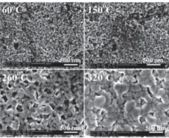
To obtain conductive structures the printing pattern must be subjected to sintering. It is in this step that surfactant, present around the NPs in solution will be removed. Making the NPs coalesce to form a continuous electrical path as Figure 1.3 shows.1,4,5,8,18,19,23
5
Figure 1.3-SEM images obtained with silver ink deposited on glass and sintered at different temperatures1
The most common method is heating the pattern on a hot plate or oven at elevated temperatures, so-called thermal sintering. For silver and copper this happens, around 200-350 ºC for 10-60 min, with the printed films achieving resistivity values comparable to that of bulk silver (1.6 × 10⁻⁸ Ωm)18 and copper.1,5,13,17,23 A problem with this is that most patterns are printed on plastic, paper or on some other kind of heat sensitive substrate which cannot handle such temperatures without damage and can lead to oxidation which reduces the conductivity. For the reasons mentioned above, other alternatives have been studied for sintering.1,4,5,8,19,23
Another well-known method is called photonic sintering, which consists on using electromagnetic radiation to sinter the printed patterns. The most common types of radiation used goes from the IR all the way to the UV part of the spectrum, in this case for silver NP ink the most effective is IR5 resulting in a resistivity 4 times higher than the bulk value.1 If the substrate is not sensitive to this kind of radiations, this method solves the problem of the high temperatures, because the energy introduced by the electromagnetic radiation is absorbed by the ink and gets confined to the NPs, having little to no effect on the substrate due to its transparency to the radiation if selected properly.1,4,5,17,23
The fact that the principle of photonic sintering is the absorption of a specific wavelength of radiation it becomes possible to make use of lasers to take this concept to the next level. By narrowing the wavelength window or even selecting a single wavelength to match the absorption spectrum of the selected ink, maximizing the efficiency of this sintering process.1,4,23 Photonic sintering is an ultra-fast process, it can be done in single or multiple flashes of radiation and is compatible with industrial processes, turning it into an attractive alternative over conventional thermal sintering.1,4,17,23
Another way to make the printed patterns conductive, in a reduced amount of time and without destroying the substrate is using a microwave oven to submit the pattern to microwave radiation5,23, which the metals are able to absorb but they have a very small penetration depth, just around of 1-2 µm for silver, gold and copper at a frequency of 2.54 GHz.1,19,23 This means that in order for this technique to be successful the thickness of the printed patterns has to be in the same range of the penetration depth.1,19,23 In the case of most metals, is possible to extend pass that limit due to the fact that they are good thermal conductors.1
Finally, other less used methods of sintering are electrical sintering, which uses Joules-effects heating to sinter the film.23 It’s done by applying a potential difference across the printed pattern creating a current which will generate a localized heating of the ink. An important thing with this method is that the pattern has to be already slightly conductive before sintering.1,23 It is also possible to use plasma sintering which is done normally by exposing the printed pattern to low-pressure argon plasma and the last one is chemical sintering which promotes the coalescence of metal NP through the use of chemical reactions that can be done at room temperature.1,5,6
7
2. Methodology
This section, describes the different materials and methodologies used to achieve the final prototype, which will have a similar structure to the Figure 2.1 (not at scale), with two printed metal layers separated by a printed electrically insulating material, with vias through the insulator at specific places where the two conductive layers need to be connected to assure circuit functionality. For the final prototype, this metallization scheme is printed on top of a glass substrate with discrete oxide TFTs.
Figure 2.1-Schematic of a cross-section of the final prototype, comprising a printed, multilevel metallization scheme on a glass substrate with discrete oxide TFTs.
2.1 Conductive layer
To fabricate the conductive layer the material chosen was a commercially available Ag ink by Sicrys. This specific product (Sicrys 150T-13) has a 50% metal loading of silver nanoparticles with a d50 value of 70 nm and a viscosity of 26 cP.
To carry out the printing of the conductive ink, it was used a Pixdro LP50 printer equipped with an assembly module compatible with Fujifilm Dimatix heads, specifically the 11610 model with 16 nozzles, spaced 254 µm, each with a diameter of 21 µm and a calibrated drop size of 10 pL.
The printer is controlled by a software with a vector image as an input from a graphic illustration program like Inkscape, which converts the black and white pattern to a printable data. To optimize the printing process towards the lowest possible electrical resistivity and highest lateral resolution a pattern was designed (Figure 2.2) using Inkscape, consisting of two lines with width of 100 and 50 µm and 1 cm between the two pads (squares of 500 × 500 µm2).
Figure 2.2- Inkscape pattern of conductive lines for optimization of the Ag printing process Next, the pattern was printed under a combination of several conditions summarized in Table 2.1, over soda-lime glass cleaned with acetone and isopropanol and dried with nitrogen gas.
Table 2.1- Summary of the different printing variables tested to achieve conductive Ag lines Substrate
temperature (ºC)
Speed (mm/s) Drops per inch (DPI) 30 1 750 50 10 1000 70 50 1500 - 100 2000 - 150 3000
8
For the calibration of the jetting process, the nozzles were heated to 31 ºC, but during printing, only one active nozzle was used. To ensure the best droplet formation a set of 3 voltages in a custom waveform were applied to the piezoelectric crystal, those where 3, 5 and 25 V, respectively.
To make the silver lines conductive, a post-printing annealing is required, so the best printing condition is select to make sure that the only thing affecting the conductivity of the lines is the annealing process.
First, a conventional thermal process on a hot plate was performed, utilizing different temperatures (180, 200, 250 and 300 ºC) over a period of 15, 30 and 60 minutes and their electrical resistance was measured.
Next, a combination of thermal and photonic annealing was tested, with a hot plate set at 180 ºC and an IR lamp (Philips BR125, with 250 W and a maximum radiation pick at a wavelength of 1100 nm) at 1 cm away from the sample, over a period of 5, 10, 15 and 30 minutes and the resistance was measured as well.
The printing on the insulating layer was done by a multi-layer approach, where the speed was kept constant at 50 mm/s and changing the DPI from 300 to 500 and the number of layers from 1 to 4. Finally, the post-treatment applied was a simple thermal annealing of 180 ºC for 30 min over a hot plate.
2.2 Insulating layer
For the insulating layer a solution of polyvinylpyrrolidone (PVP) from Sigma-Aldrich (CAS: 9003-39-8) with an average molecular weight of 10000, was prepared by mixing 2 g of PVP in 10 mL of ethanol and stirred for 4 hours.
To deposit the PVP solution a shear casting system (K101 control coated system) was used. The system utilizes a heated bed with a temperature control that was set to ambient temperature and 30 ºC. The speed of the deposition was also evaluated (1 and 2 mm/s), as well as the number of layers (1 and 2 layers) and direction of coating, to see which condition gives the best thickness and uniformity.
To make sure that the solvent was evaporated and the PVP has hardened, the films were baked in a hot plate at 180 ºC for 30 min.
2.3 Via formation by laser ablation
To create vias through the insulating layer a Universal Laser System CO2 VLS 3.5 operating in the infrared region of 10.6 µm was employed. Plano-convex lens of type 2.0” with focal length of 50.8 mm, focus point of 0.127 mm and depth of focus of 2.54 mm were utilized to focus the laser beam and keep the performance constant for all the tests.
The laser system was controlled using a vector image input from Adobe Illustrator, defined in the form of red, green and blue (RGB) colour map. Raster mode was selected to work at the surface of the material, meanwhile, nitrogen gas was used to cool down the sample during the process. To remove the PVP solution the speed of the laser was kept at 1 % and only the power and the pulses per inch (PPI) were changed from 1 to 3 % and from 1000 to 800 respectively.
2.4 Characterization methods (morphological and electrical analysis)
All the silver lines were observed under an optical microscope (Olympus BX51) and their width and thickness were measured using Image J software and profilometer (Ambios XP-200 plus) equipped with a diamond stylus tip, respectively. The electrical measurements to extract the I-V curves were carried out using a semiconductor parameter analyser (Agilent 4155C) and a microprobe station (Cascade M150) at room temperature and in the dark. IV-curves were taken for conductive lines in a single layer, for conductive lines containing the two metal layers (through a via in PVP), as well as for the metal-insulator-metal stack to access the breakdown field of the insulating material.
The thickness and uniformity of the PVP films were measured by the same profilometer mentioned above.
To optimize the laser ablation process on PVP vias were examined by a benchtop scanning electron microscope equipped with an energy dispersive detector (SEM-EDS, Hitachi TM
9
3030plus Tabletop), as well as by the electrical measurements of conductive lines for the two metal lines contacted trough a PVP via, as previously mentioned.
2.5 Final prototype
After the oxide TFTs were produced and passivated in clean room environment, the digital circuit blocks are selected and the metallization patterns are designed to be printed following these steps: i) the first metal layer is printed with a resolution of 400 DPI, a speed of 50 mm/s with three printing layers; ii) This layer is annealed at 200 ºC for 30 min and other sample is sintered for 5 min under an IR lamp for comparative effects; iii) The PVP solution is deposited with two layers (with the second layer being deposited in the opposite direction with respect to the first layer) at a 1 mm/s speed, with the substrate temperature of 30 ºC and finally cured at 180 ºC for 30 min; iv) The second metallization layer is printed and annealed exactly as the first one.
The circuits are characterized in the DC domain using the same semiconductor analyser and the probe station described in 2.4.
11
3. Results and discussion
3.1 Printing process
3.1.1 Inkjet printing silver lines on glass substrate
This section discusses the effects of different variables on the printing process. To narrow down the most useful values for those variables a quick and general study of all the parameters was performed.
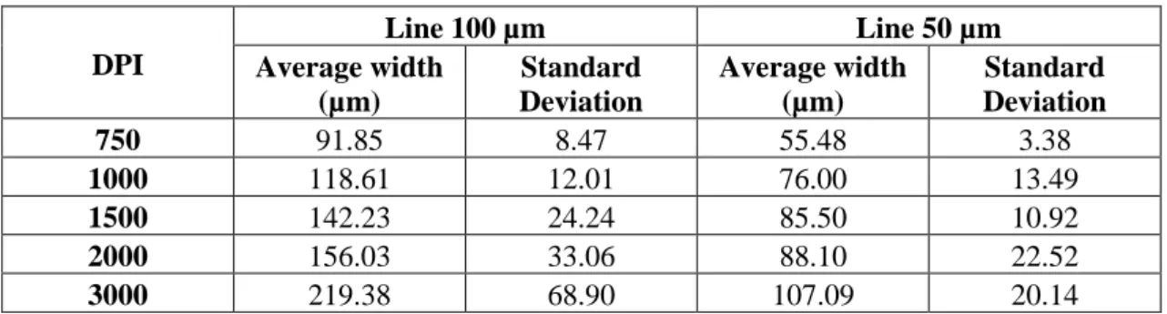
The first parameter studied was the resolution measured in drops per inch (DPI), keeping the speed constantly at 150 mm/s and no substrate heating. The results, in terms of the linewidth, can be observed in the table below.
Table 3.1- Results of the effect of the DPIs in the morphology of the printed Ag lines.
DPI Line 100 µm Line 50 µm Average width (µm) Standard Deviation Average width (µm) Standard Deviation 750 91.85 8.47 55.48 3.38 1000 118.61 12.01 76.00 13.49 1500 142.23 24.24 85.50 10.92 2000 156.03 33.06 88.10 22.52 3000 219.38 68.90 107.09 20.14
From the Table 3.1 it is easy to conclude that the 750 DPI is the best for both set of lines, but as the figure below shows both 50 (Figure 3.1a)) and 100 µm (Figure 3.1d)) lines are not continuous which is not useful for the final objective of achieving transistors interconnections.
Figure 3.1-Effect of the resolution in the morphology of the printed Ag lines; a) to c) 50 µm lines with 750, 1000 and 1500 DPI respectively; d) to f) 100 µm lines with 750, 1000 and 1500
DPI respectively.
To solve that the best way would be to increase the DPI and from the Figure 3.1b) and e) it is possible to observe that the gaps between the droplets are smaller, so if the DPIs are increased to 1500 the set of 100 µm lines (Figure 3.1f)) are now continuous due to being deposited more ink. However, for the set of 50 µm lines (Figure 3.1c)) it is still a problem, which means that there are other variables that need to be considered, like the printing speed and the substrate temperature. Another problem with 1500 DPIs is that significant bulges start appearing and from the Table 3.1 it is possible to see an increase in the average width and standard deviation, so probably the best values to be used in the future would be 750 and 1000 DPIs.
12
The next parameter studied was the speed of the printing plate measured in mm/s. For this end, DPI was set to 1000 and the temperature of the substrate at around 22 ºC (laboratory temperature). The table below shows the results of the different speed values tested.
Table 3.2- Results of the effect of the printing speed in the morphology of the printed Ag lines.
Speed (mm/s) Line 100 µm Line 50 µm Average width (µm) Standard Deviation Average width (µm) Standard Deviation 100 108.25 4.97 73.55 7.69 50 128.22 16.50 100.40 39.26 10 129.17 11.87 88.25 21.97 1 139.46 13.38 92.69 26.98
These results shows that the 100 mm/s speed is the best for both lines, but as the Figure 3.2a) and Figure 3.2d) demonstrate the problem of discontinuities in the lines it is still present, like in the previous test. Slowing down the speed solves this problem but this creates even bigger bulges, which is confirmed by the increase in the standard deviation as well in Figure 3.2b), c) and e).
Figure 3.2- Effect of the printing speed in the morphology of the printed Ag lines a) to c) 50 µm lines with a printing speed of 100, 50 and 10 mm/s respectively; d) to f) 100 µm lines with a
printing speed of 100, 50 and 10 mm/s respectively.
Another observation from Table 3.2 is that for the 100 µm line both 50 and 10 mm/s originated the same results, eliminating the 10 mm/s setting because does not constitute an advantage using a lower speed. Meanwhile, the 1 mm/s speed is the worst of all the conditions tested. In the case of the 50 µm line, the results are inconclusive due to a high DPI value.
These results show that the higher the speed the bigger the resolution to achieve the same printing results. For that reason, different combinations between 100 and 50 mm/s speed and 750 and 1000 DPI resolution will be analysed further.
Finally, the substrate temperature was tested, keeping the speed set at 100 mm/s and resolution at 1000 DPIs. The results are summarized in the table below.
13
Table 3.3- Results of the effect of the substrate temperature in the morphology of the printed Ag lines. Substrate temperature (ºC) Line 100 µm Line 50 µm Average width (µm) Standard Deviation Average width (µm) Standard Deviation 30 106.60 3.31 72.33 4.04 50 105.75 6.97 67.09 4.31 70 115.79 10.35 80.19 10.11
An increase in the substrate temperature improves the uniformity of the printed lines, represented by a significant decrease in the standard deviation (Table 3.3). A problem is when setting the substrate to 70 ºC causes an increase in the nozzle temperature, which in turn causes printing instabilities and errors. By leaving the physical properties of the ink outside the excepted ranges of the inkjet printing, for those reasons 70 ºC it will not be used.
Figure 3.3- Effect of the substrate temperature in the morphology of the printed Ag lines a) to c) 50 µm lines with a substrate temperature of 30, 50 and 70 ºC respectively; d) to f) 100 µm lines
with a substrate temperature of 30, 50 and 70 ºC respectively
From Figure 3.3 b) and Figure 3.3 e) it is possible to observe that the substrate temperature helps in solving the broken lines problem. This is justified by the temperature allowing the droplets to merge together. Nevertheless since 30 and 50 ºC are so similar, in terms of line width, both will be tested in the next phase.
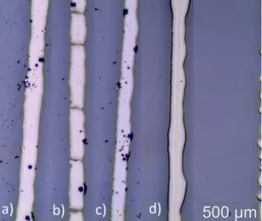
In conclusion, in the next phase of testing the best parameters for each variable (attachment B) were combined, only one layer of ink printed and the effects, on the electrical resistivity quantified. To turn the Ag lines electrically conductive it is necessary to apply a sintering process, for example setting a hot plate at 180 ºC for 30 min, which is recommended by the ink supplier. To simplify the understanding of the results, the 100 µm lines are the first to be studied. The printing conditions are substrate temperature set at 30 ºC, while speed and DPI vary, for each condition the resistance and the geometrical parameters (width and thickness) were measured and summarized in Table 3.4.
14
Table 3.4-Electrical resistivity for the 100 µm line with the substrate temperature of 30 ºC with different speeds and DPIs
Condition Width (µm) Thickness (nm)
Resistance (Ω) Resistivity (Ωm) Speed (mm/s) DPI Average Standard deviation Average Standard deviation 100 750 120.53 6.53 954.22 203.85 110.60 1.27 × 10 -6 1000 111.70 7.86 935.67 126.79 >109 >10 50 750 113.83 9.31 941.56 126.76 41.17 4.41 × 10 -7 1000 113.13 10.29 1153.22 169.51 20.34 2.65 × 10⁻⁷ One result to highlight it is the second printing condition (speed of 100 mm/s and 1000 DPI) that has an electrical resistance greater than 109 Ω, this mean that the line was not conductive and the reason is represented in Figure 3.4b), which shows that the line is interrupted preventing the flow of current.
The last condition (speed of 50 mm/s and 1000 DPI) is the best one by having the lowest electrical resistivity. This can be justified by the fact that the line has the biggest cross-sectional area, due to an increase in thickness, caused by an increase in the amount of ink being deposited.
Figure 3.4- 100 µm Ag line printed with a substrate temperature of 30 ºC; a) speed of 100 mm/s and 750 DPI; b) speed of 100 mm/s and 1000 DPI; c) speed of 50 mm/s and 750 DPI; d) speed
of 50 mm/s and 1000 DPI
This increase in ink is useful for lowering the electrical resistivity but can cause deformations, like bulges, in the line as it can be observed in Figure 3.4d). So, an optimization must be achieved between the electrical properties and morphology of the line. In this context the best condition is the one with 50 mm/s speed and 750 DPI (Figure 3.4c)).
Figure 3.4 also shows some blue dots, this is unseen impurities at the time of printing and sintering, but they didn’t influence the results because different parallel samples obtained the same results without impurities.
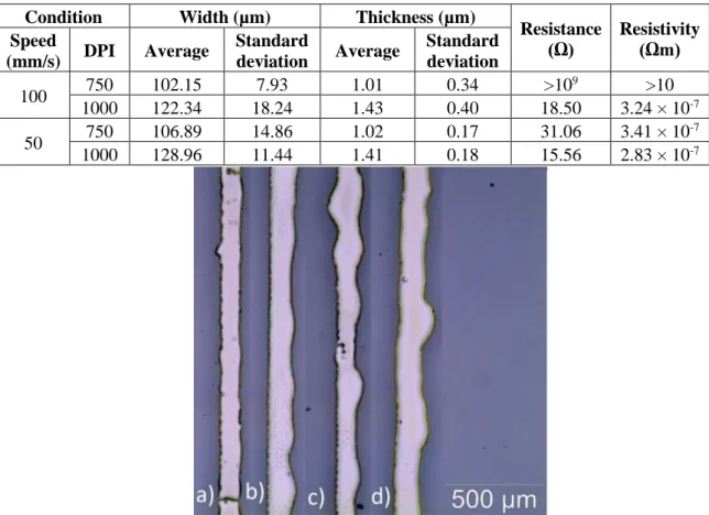
By changing the substrate temperature to 50 ºC it was possible to obtain consistent electrical performances across different printing conditions, as Table 3.5 confirms. This is due to an, expected, increase in thickness because as the droplets encounter a hotter substrate, this promotes a faster evaporation of the solvent, which leads to a faster solidification of those droplets instead of spreading. Another effect is the increase in lateral resolution of the printed lines, as expected, by allowing the printed lines to have a smaller width closer to the printing pattern.
15
Table 3.5- Electrical resistivity for the 100 µm line with the substrate temperature of 50 ºC with different speeds and DPIs
Condition Width (µm) Thickness (µm)
Resistance (Ω) Resistivity (Ωm) Speed (mm/s) DPI Average Standard deviation Average Standard deviation 100 750 102.15 7.93 1.01 0.34 >10 9 >10 1000 122.34 18.24 1.43 0.40 18.50 3.24 × 10⁻⁷ 50 750 106.89 14.86 1.02 0.17 31.06 3.41 × 10 -7 1000 128.96 11.44 1.41 0.18 15.56 2.83 × 10⁻⁷
Figure 3.5- 100 µm Ag line printed with a substrate temperature of 50 ºC; a) speed of 100 mm/s and 750 DPI; b) speed of 100 mm/s and 1000 DPI; c) speed of 50 mm/s and 750 DPI; d) speed
of 50 mm/s and 1000 DPI
When analysing Figure 3.5c) it is possible to see deformations that previously did not exist, as an increase in the standard deviation also confirms. This is due to a high humidity content (superior to 50 %) in the air or due to instabilities of the printing nozzle, caused by wear of the piezoelectric crystal. The effect of all this are changes to the jetting and droplet formation causing instabilities on the falling droplets, as Figure 3.6 shows.
Figure 3.6- Time-lapse of the droplet formation under 50 % humidity environment As the droplets form and fall, they start getting affected by the ambient conditions and if not controlled the effect can be so dramatic that the droplet breaks and disappears like what happens when going from Figure 3.6c) to Figure 3.6d), which causes unpredictability in the printing prosses.
To reduce or even sometimes cancel this effect it is possible to change the voltage values that control the piezoelectric response of the crystal responsible for producing the droplets. However, as attachment C shows, this is not the optimal solutions because the droplet tail can
16
cause another set of problems like unwanted amounts of ink or little satellite droplets in the substrate.22
In summary, despite the jetting problems, for the 100 µm lines the best printing conditions are setting the substrate temperature to 50 ºC and print with 50 mm/s speed and 750 DPI because it has the smallest width while maintaining a good electrical performance.
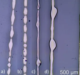
Since the inkjet process is very sensitive to changes, from the design of the pattern to the environment conditions in the lab, it is necessary to confirm that changing the width from 100 to 50 µm the conclusions already discussed, stay the same. For that reason, the exact same parameters and conditions where re-tested for this new linewidth. The electrical and geometrical results are summarized in Table 3.6, Table 3.7, Figure 3.7 and Figure 3.8.
Table 3.6- Electrical resistivity for the 50 µm line with the substrate temperature of 30 ºC with different speeds and DPIs
Condition Width (µm) Thickness (µm)
Resistance (Ω) Resistivity (Ωm) Speed (mm/s) DPI Average Standard deviation Average Standard deviation 100 750 68.49 9.93 Not measured >10 9 >10 1000 70.27 7.36 Not measured >109 >10 50 750 64.98 13.57 Not measured >10 9 >10 1000 77.35 14.19 1.11 0.14 39.39 3.38 × 10⁻⁷
The first three conditions have an electrical resistance bigger than the equipment limit, the printed lines are considered not to be electrically conductive, for that reason the thickness was not measured.
Figure 3.7- 50 µm line printed with a substrate temperature of 30 ºC; a) speed of 100 mm/s and 750 DPI; b) speed of 100 mm/s and 1000 DPI; c) speed of 50 mm/s and 750 DPI; d) speed of 50
17
Table 3.7- Electrical resistivity for the 50 µm line with the substrate temperature of 50 ºC with different speeds and DPIs
Condition Width (µm) Thickness (µm)
Resistance (Ω) Resistivity (Ωm) Speed (mm/s) DPI Average Standard deviation Average Standard deviation 100 750 55.85 13.87 Not measured >109 >10 100 1000 71.12 10.15 1.13 0.32 31.96 2.57 × 10⁻⁷ 50 750 66.50 12.57 0.62 0.18 143.55 5.96 × 10⁻⁷ 50 1000 65.39 8.52 1.02 0.12 38.15 2.54 × 10⁻⁷
Figure 3.8- 50 µm line printed with a substrate temperature of 50 ºC; a) speed of 100 mm/s and 750 DPI; b) speed of 100 mm/s and 1000 DPI; c) speed of 50 mm/s and 750 DPI; d) speed of 50
mm/s and 1000 DPI
For the case of 50 µm lines the exact same conclusions as the 100 µm can be observed and confirms that changing the printing pattern doesn’t have a significant effect on the performance of the Ag lines. Since the same printing conditions is able to print lines with a balance between cross-sectional area and electrical performance for both set of lines, the overall process can be simplified because it is possible to change the width of the lines depending on the performance needed without changing printing conditions.
3.1.2 Deposition of PVP
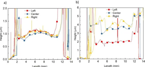
The deposition of the PVP solution accomplished with shear casting was studied with the objective of obtaining a uniform layer with a minimum thickness of 1 µm to guaranty the insulation between multiple conductive layers. Figure 3.9 represents the profile obtained when different shear casting speeds (1 mm/s and 2 mm/s) were applied.
18
Figure 3.9- Profile taken at three different points of the insulating PVP layer obtained with two different shear casting speeds; a) 1 mm/s; b) 2 mm/s
From the figure above it is possible to observe that 2 mm/s speed (Figure 3.9b)) deposits a film with the required thickness but it is not uniform or consistent. This effect is due to a low viscosity of the insulating PVP solution, causing a worst control over the deposition process. In the case of 1 mm/s speed (Figure 3.9a)) the thickness is lower than required, making it unusable.
To solve this samples with two layers were deposited and the results are represented in Figure 3.10.
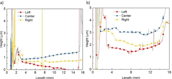
Figure 3.10- Profile taken at three different points of the insulating PVP layer obtained with two different shear casting speeds and printed twice; a) 1 mm/s speed; b) 2 mm/s speed From the profile, it is possible to observe that the difference in thickness across the samples from left to right is minimal but across the length it is still a problem. In the first sample (Figure 3.10a)) the ascending profile prevents this condition to be useful by complicating the laser etching process, explained in section 3.4. However in the 2 mm/s sample (Figure 3.10b)) the thickness is unnecessarily tick and the profile exhibits more scattering than the 1 mm/s sample, which could present a problem to effectively print the second conductive layer.
Since the PVP solution is alcohol-based, introducing temperature to the process allows a faster hardening of the PVP, by helping with solvent evaporation and wettability. This together with depositing the second layer in the opposite direction with respect to the first layer will allow to reduce the ascending profile observed while keeping the uniformity of the profile across the sample, as Figure 3.11 shows.
19
Figure 3.11- Profile taken at three different points of the insulating PVP layer deposited twice, with the second layer deposited in the opposite direction with respect to the first one and with
two different shear casting speeds at 30 ºC; a) 1 mm/s speed; b) 2 mm/s speed
From the profile of Figure 3.11b) it was not possible to keep the uniformity of the insulating layer, as desired for consistent and reproducible performance, because the deposition occurs too fast (coupled with the small variations introduced by the equipment) for allowing the deposition to occur predictability. Even though the thickness is sufficient for the desired application that problem with the uniformity of the profile, turns it unfit for the final application. Meanwhile in Figure 3.11a) is possible to observe the desired uniform profile, even with few defects, but less thickness than required, so the solution found was to add more PVP solution.
Figure 3.12- Profile of two parallel samples of insulating PVP layer deposited twice, with the second layer deposited in the opposite direction with respect to the first one, at 1 mm/s shear
casting speed and 30 ºC.
From Figure 3.12 it is possible to observe that adding a larger volume of PVP solution solved the problem of insufficient thickness. The two parallel samples (r1 and r2) have the same profile and average thickness across the entire sample. Since the objective was to have a minimum thickness of 1 µm, with these conditions it was possible to have a thickness of 4 µm, which is enough to prevent short circuits between the two conductive layers.
3.1.3 Inkjet printing silver lines on PVP substrate
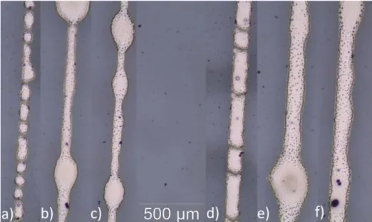
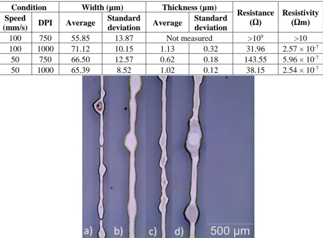
After depositing the insulating layer, a new conductive layer is printed but now on top of PVP, which naturally has different surface properties compared to glass, like surface energy, contact angle and wettability. Which means that the previous printing conditions would not achieve the same results as in section 3.1.1, as Figure 3.13 and Table 3.8 shows.
20
Figure 3.13- Ag lines printed on PVP with substrate temperature of 50 ºC, speed of 50 mm/s and 750 DPI a) 50 µm line b) 100 µm line.
Table 3.8- Width of Ag lines printed on PVP with substrate temperature of 50 ºC, speed of 50 mm/s and 750 DPI.
Line Width (µm)
Average Standard deviation
100 µm 229.28 3.62
50 µm 186.11 5.31
Using the previous printing conditions causes a dramatic increase in the width of both lines, 114 % for 100 µm and 180 % for 50 µm line. This can be justified by the PVP having better wettability than glass, which is very useful to decrease the line edge roughness of the printed lines. However, the final prototype requires the line width to be the smallest possible, so new printing conditions must be utilized. These new printing conditions are based on decreasing the DPI and adding more printing layers, allowing the printed lines to have enough material to be electrically conductive but without having poor line edge roughness. All lines were printed using substrate temperature of 50 ºC and speed of 50 mm/s, changing only the DPI and the number of printed layers. The sintering method was 180 ºC for 30 min.
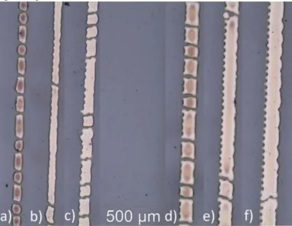
The morphological and electrical performance results for the 100 µm lines are shown in Table 3.9 and Figure 3.14.
Table 3.9- Electrical resistivity for the 100 µm line with different DPIs and number of printed layers.
Condition Width (µm) Thickness (nm)
Resistance (Ω) Resistivity (Ωm) DPI Number of layers Average Standard deviation Average Standard deviation 300 3 265.11 61.10 300.89 60.73 89.01 7.10 × 10 -7 4 281.24 22.22 334.33 24.14 177.13 1.67 × 10⁻⁶ 400 2 160.34 6.74 436.78 25.55 >10 9 >10 3 202.66 13.08 504.78 44.38 25.70 2.63 × 10⁻⁷ 500 1 255.51 17.91 153.22 7.64 1403.00 5.49 × 10 -6 2 242.37 23.94 307.00 38.50 648.52 4.83 × 10⁻⁶
21
Figure 3.14- 100 µm Ag lines printed on PVP with a substrate temperature of 50 ºC and speed of 50 mm/s.
Even with this new printing conditions, the linewidth remains outside the requirements for the final prototype. This problem is solved by reducing the linewidth in the computer software, as it was tested in later stages of this work.
Since the different layers were printed without stopping in between layers, combined with a high substrate temperature and a low volume of ink. This causes a faster evaporation of the solvent, which results in a faster solidification of the droplets of ink preventing the merging of those droplets and subsequently the different layers. This fact explains the unexpected increase in electrical resistivity when comparing the two printing conditions with 300 DPI.
When the DPI increases to 400 and three layers are printed, it is possible to obtain the lowest electrical resistivity (2.63 × 10⁻⁷ Ωm) and when compared to the best electrically performing printed line on glass (3.41 × 10⁻⁷ Ωm), it is possible to obtain comparable electrical resistivities.
Regarding the 50 µm wide lines, they demonstrate the same effects already discussed above for the 100 µm lines, concluding that 400 DPI with three printed layers is the best printing condition, as attachment D and attachment E shows.
In conclusion, the printing on PVP clearly shows one of the major challenges of inkjet printing, which is when changing one parameter of the process the conditions must be re-tested and most of the time new printing conditions have to be introduced. For example, if the dielectric layer has a different material, the surface properties have to be considered and the printing conditions optimized for this new material.
3.2 Sintering methods
3.2.1 Thermal annealing
This section describes the effects of the annealing temperature coupled with the duration of the annealing process. This study is carried out with a glass substrate and utilizing the best printing conditions found in section 3.1.1 (substrate temperature of 50 ºC, 750 DPI and 50 mm/s speed).
The sintering conditions to be studied are four different temperatures (180, 200, 250 and 300 ºC) for three different times (15, 30 and 60 min) on a hot plate, the different resistivities were calculated and represented in Figure 3.15