Miguel Diogo Furtado Alexandre
Licenciado em Engenharia de Micro e Nanotecnologias
Theoretical Study of Optimum Luminescent
Down-Shifting Properties for High Efficiency
and Stable Perovskite Solar Cells
Dissertação para obtenção do Grau de Mestre em
Engenharia de Micro e Nanotecnologias
Orientador: Manuel J. Mendes, Post-Doc Fellow and Invited Assis-tant Professor,
Faculty of Sciences and Technology, NOVA University of Lisbon
Co-orientador: Rodrigo Martins, Full Professor,
Faculty of Sciences and Technology, NOVA University of Lisbon
Júri
Presidente: Dr. Hugo Manuel Brito Águas
Arguente: Dr. Maria Rute de Amorim e Sá Ferreira André Vogal: Dr. Manuel João de Moura Dias Mendes
Theoretical Study of Optimum Luminescent Down-Shifting Properties for High Efficiency and Stable Perovskite Solar Cells
Copyright © Miguel Diogo Furtado Alexandre, Faculdade de Ciências e Tecnologia, Uni-versidade NOVA de Lisboa.
A Faculdade de Ciências e Tecnologia e a Universidade NOVA de Lisboa têm o direito, perpétuo e sem limites geográficos, de arquivar e publicar esta dissertação através de exemplares impressos reproduzidos em papel ou de forma digital, ou por qualquer outro meio conhecido ou que venha a ser inventado, e de a divulgar através de repositórios científicos e de admitir a sua cópia e distribuição com objetivos educacionais ou de inves-tigação, não comerciais, desde que seja dado crédito ao autor e editor.
Este documento foi gerado utilizando o processador (pdf)LATEX, com base no template “novathesis” [1] desenvolvido no Dep. Informática da FCT-NOVA [2].
Ac k n o w l e d g e m e n t s
Em primeiro lugar, gostaria de agradecer ao Professor Rodrigo Martins e à Professora Elvira Fortunato, por terem sido os fundadores deste magnífico curso onde estive nos últimos 5 anos, que me levou à descoberta de novas áreas, culminando no trabalho que aqui apresento.
Gostaria também de agradecer ao meu orientador, Professor Manuel Mendes, e co-orientador, Professor Rodrigo Martins, pela oportunidade de fazer uma tese na área dos fotovoltaicos, que é um tema de significante interesse para mim. Aos nomes anteriores, gostaria também de adicionar o Professor Hugo Águas e o Mestre Sirazul Zakir, pela ajuda e orientação que me deram durante este processo.
Não posso também deixar de fora todos os professores que, ao longo de todos os meus anos de ensino, me ajudaram a adquirir o conhecimento que hoje possuo, sendo que este trabalho não teria sido possível sem as suas contribuições.
Um obrigado muito especial para a minha família que sempre me suportou em todos os desafios que tive ao longo dos anos. Em especial, gostaria de mencionar o meu pai, a minha mãe e a minha irmã, que sempre foram as primeiras pessoas a ajudar-me a ultrapassar os problemas que tive, assim como, pelo seu esforço, também me permitiram que tivesse tido estes últimos 5 anos que significaram muito para mim.
Gostaria também de agradecer aos meus colegas Fábio Vieira e Manuel Chapa, com quem tive uma excelente semana para escrutinar teses, que ajudou a colmatar muitas das lacunas e bengalas que temos na escrita.
Por fim, mas não menos importante, gostaria também de agradecer aos meus amigos, com quem passei excelentes momentos ao longo destes últimos anos. Em especial, destaco os nomes João Teles, Manuel Chapa, Fábio Vieira, Débora Magalhães, João Pina, Ricardo Viana e Catarina Marques, Ana Pinheiro, Rita Fragoso e Maria Helena, sendo estas as pessoas com quem me dei mais.
A b s t r a c t
In recent years, the discovery of the excellent optical and electrical properties of per-ovskite materials made them one of focus of research in the area of photovoltaics, with its efficiency increasing significantly since its inception, in 2009. However, problems
associated with the stability of these materials have hindered their widescale market ap-plication, with two examples being the UV degradation of the absorber material and the photoactivity, under 400 nm wavelengths, of TiO2 which is one of the main materials
used as an electron transport layer in these cells. Consequently, different methods were
studied to minimize this degradation. One example consists in using down-shifting ma-terials that change the harmful UV radiation to higher wavelengths that have no effect on
the cell stability. Thus, this work is focused in the theoretical study of the photocurrent gains that can be attained by emulating the changed spectrum resulting from applying these materials, as well as the reduction in the harmful effects of UV radiation on
per-ovskite solar cells. This first case analyzed resulted in gains of around 1% for planar cells and around 2% for cells with photonic structures. For the second optimized case, one was able to obtain a general reduction in generation in TiO2of one order of magnitude,
coupled with a 80% reduction of perovskite’s UV absorption.
Keywords: Photovoltaics, Photonic-enhanced Perovskite Solar Cells, Ultraviolet Stability,
Down-shifting, Light Trapping
R e s u m o
A recente descoberta das excelentes propriedades óticas e elétricas das perovskites, para aplicações em células solares, fez com que se tornassem num dos principais alvos de estudo na área dos fotovoltaicos, levando ao rápido aumento da sua eficiência desde que foram introduzidas. Contudo, problemas associados com a estabilidade destes materiais tem limitado a sua implementação à larga escala. Alguns exemplos são a degradação do material fotoativo quando exposto a radiação UV, assim como a fotoatividade do TiO2,
para comprimentos de onda inferiores a 400 nm, uma vez que este se trata de um dos materiais mais usados como camada de transporte de eletrões nestas células. Consequen-temente, diferentes métodos estão a ser estudados, de forma a minimizar esta degradação. Um exemplo, consiste em fazerdown-shiftingda radiação solar de forma a mudar a nefasta radiação UV para comprimentos de onda que não impactem a perovskite negativamente. Desta forma, este trabalho foca-se no estudo teórico dos ganhos de corrente gerada na célula devido à aplicação dedown-shifting, em conjunto com os efeitos na nefasta geração no TiO2. No primeiro caso, ganhos de cerca de 1% foram obtidos para células planares e
cerca de 2% para células com estruturas fotónicas. Para o segundo caso otimizado obteve-se uma redução de uma ordem de grandeza na geração no TiO2e uma redução de 80%
para a radiação UV absorvida pela perovskite.
Palavras-chave: Fotovoltaicos, Células Solares de Perovskite com Estruturas Fotónicas,
Estabilidade à Radiação Ultravioleta, Down-shifting, Aprisionamento de Luz
C o n t e n t s
List of Figures xv
List of Tables xix
Symbols xxi
Acronyms xxiii
Motivation and Objectives xxv
Work Strategy xxvii
1 Introduction 1
1.1 Solar Cell Market . . . 1
1.2 Perovskite Solar Cells . . . 1
1.3 Luminescent Down-Shifting . . . 3
1.4 Dielectric Photonic Structures . . . 4
1.5 Finite-Difference Time-Domain Simulation . . . . 4
2 Simulation Setup 7 2.1 Solar Cell Structure . . . 7
3 Results and Discussion 9 3.1 Optical simulation . . . 9
3.2 Down Shifted Spectrum . . . 10
3.3 Planar Perovskite Solar Cells . . . 10
3.3.1 Reflection Profiles . . . 11
3.3.2 Absorption Profiles . . . 13
3.3.3 Photocurrent Shifts . . . 15
3.3.4 Generation Profiles and UV absorption . . . 18
3.4 Solar Cells with Dielectric Photonic Structures . . . 20
3.4.1 Reflection Profiles . . . 22
3.4.2 Absorption Profiles . . . 22
3.4.3 Photocurrent Shifts . . . 23
CO N T E N T S
3.4.4 Generation Profiles . . . 26 3.5 Final Thoughts . . . 27
4 Conclusion and Future Perspectives 29
References 31
I Equations for the FDTD method 39
II Simulation Parameters 41
III Simulated Transmissions 43
L i s t o f F i g u r e s
1.1 Unit cell for the basic ABX3perovskite structure. The circle sizes represent
the different ion radius, meaning the A ion is the largest and the X ion the
smallest. The colors refer to the different ions used. MA, EA and FA stand for
methylammonium, ethylammonium and formamidinium, respectively. . . . 2
1.2 Schematic of the main PSCs architectures. a) cell with n-i-p configuration and mesoporous layer, b) cell with n-i-p configuration and c) cell with p-i-n configuration. . . 3
1.3 Schematic representation of the Yee algorithm. On the left is shown the Yee cell with the various corresponding fields. The direction of the fields in each face is chosen to satisfy Faraday’s law. On the right, is shown the field with the full notation, including the spatial coordinates for the top face of the cube. . 5
2.1 Schematic of the solar cells used in the simulations. a) Cell with planar struc-ture, PC, used as reference and b) Cell with light trapping structures, LTC. The dimensions of the cell on the right refer to their respective counterparts in Table 2.1. The different layers properties are shown in Annex II. . . 8
3.1 a) In solid line are the absorbed and emitted fluxes forλC of 350 nm and∆λof
200 nm. In dash line is the gaussian profile used to calculate the absorbed and emitted fluxes; b) Modelled spectra transmitted through a window prototype with varying QD properties and quantum yield of 50%. Adapted from refer-ence [40]; c) Schematic of the DS process, where higher wavelength radiation is redshifted. . . 11
3.2 Resulting irradiance plots of the DS process used to simulate the effect of a LDS
layer. a) AM1.5G spectrum, in black, and 2 examples of resulting spectrums when the ∆λ remains constant as 310 nm and λ
C changes from 300 nm to
400 nm, in red and blue, respectively, b) AM1.5G spectrum, in black, and 2 examples of the resulting spectrums whenλC remains constant at 300 nm and
∆λvaries from 205 nm to 400 nm, in red and blue, respectively. . . 12
L i s t o f F i g u r e s
3.3 Reflection profiles with the results from the numerical simulation, in black, and the results from the theoretical simulation, in red. Inset is represented the modulus of the difference between the two methods. a) PC with 250 nm
perovskite, b) PC with 500 nm perovskite, c) PC with background index of 1.5 and 250 nm perovskite, d) PC with background index of 1.5 and 500 nm perovskite. . . 13 3.4 Absorption profiles with the absorption on the perovskite layer, in black; the
TiO2layer, in red; and the total cell absorption, in green. The inset profiles
show the plots for the absorbed power density through the cell volume for spe-cific wavelengths, indicated by the arrows. The leftmost graph is the absorbed power for 350 nm and the rightmost graph is the absorbed power for 900 nm. a) and b) PC with VBI for 250 nm and 500 nm perovskite, respectively; c) and d) PC with PBI for 250 nm and 500 nm perovskite, respectively. . . 15 3.5 Contour plots for the sweeps whereλC and∆λwere varied from 300 nm to
400 nm and 100 nm to 400 nm, respectively. a) PC with VBI for 500 nm per-ovskite layer and b) PC with VBI for 250 nm perper-ovskite layer. The thicker line represents the contour corresponding to the photocurrent value obtained for the pristine spectrum. The indicated values represent the respective contour photocurrent value. The topmost value refers to the contour representing the pristine value, while the bottommost refers to the highest value contour in the plot. . . 16 3.6 Contour plots for the sweeps whereλC and∆λwere varied from 300 nm to 400
nm and 100 nm to 400 nm, respectively. a) PC with PBI for 500 nm perovskite layer, b) PC with PBI for 250 nm perovskite. The thicker line represents the contour corresponding to the photocurrent value obtained for the pristine spectrum. The indicated values represent the respective contour photocurrent value. The topmost value refers to the contour representing the pristine value, while the bottommost refers to the highest value contour in the plot. . . 17 3.7 Generation profiles for the PCs with VBI. a) cell with 250 nm perovskite; b)
cell with 250 nm perovskite and optimized spectrum; c) cell with 500 nm perovskite; d) cell with 500 nm perovskite and optimized spectrum. The arrows and ellipse mark the biggest changes in the plots. . . 20 3.8 Generation profiles for the PCs with PBI. a) cell with 250 nm perovskite; b)
cell with 250 nm perovskite and optimized spectrum; c) cell with 500 nm perovskite; d) cell with 500 nm perovskite and optimized spectrum. The arrows and ellipse mark the biggest changes in the plots. . . 21 3.9 a) Reflection profile for the LTC, in black; and for the PC, in red; where both
have a 250 nm layer of perovskite absorber material. b) Reflection profile for the LTC, in black; and for the PC, in red; where both have a 500 nm perovskite absorber material. . . 22
L i s t o f F i g u r e s
3.10 a) Absorption profile for the LTC with 250 nm perovskite layer, b) absorption profiles for the LTC with 500 nm perovskite layer. The shaded areas represent the absorption of the TiO2, in red; and the remaining materials absorption, in
green. The black curve is the perovskite absorption. The inset plots represent the absorbed power density for each respective cell for a wavelength of 350 nm, bottom graph, and 900 nm, top graph. . . 24 3.11 Contour plots for the sweeps whereλC and∆λ were changed from 300 nm
to 400 nm and 100 nm to 400 nm, respectively. a) Plot for the cell with 250 nm perovskite layer and b) plot for the cell with 500 nm perovskite layer. The thicker line represents the contour corresponding to the photocurrent value obtained for the pristine spectrum. The indicated values represent the re-spective contour photocurrent value. The topmost value refers to the contour representing the pristine value, while the bottommost refers to the highest value contour in the plot. . . 25 3.12 Generation profiles for the LTC. a) cell with 250 nm perovskite; b) cell with
250 nm perovskite and optimized spectrum; c) cell with 500 nm perovskite; d) cell with 500 nm perovskite and optimized spectrum. The arrows point to the biggest plot changes. . . 27 3.13 a) Bar chart summarizing the pristine (red) and optimized (blue) Jph values
obtained from the photocurrent sweeps; b) Bar chart summarizing the Jphfor
wavelengths ranging from 300 nm to 400 nm for the for the pristine (red) and optimized spectrum (blue). . . 28
II.1 Refractive index, n, and extinction coeficient, k, for the different material used
in the simulations. These values are provided by reference [80]. . . 41
III.1 Simulated and theoretical transmission for the planar cells. a) 250 nm per-ovskite and b) 500 nm perper-ovskite. . . 43 III.2 Simulated and theoretical transmission for the planar cells with a background
index of 1.5. a) 250 nm perovskite and b) 500 nm perovskite. . . 44 III.3 Simulated transmission for the cells with photonic structures and a
back-ground index of 1.5. a) 500 nm perovskite and b) 250 nm perovskite. . . 44
L i s t o f Ta b l e s
2.1 PC and LTC parameters. Ag, Spiro and ITO represent the respective material thicknesses. TiO2, for the PC, represents the TiO2thickness and for the LTC
is the TiO2thickness between perovskite and the structures beginning. tV oids
is the structures’ TiO2 thickness. R is the voids x and y radius, while Rz is
the z radius. tV oids is the distance between the center of 2 consecutive void
structures, being given in function of R. . . 8
3.1 Summary of the optimized results obtained for the different PCs simulated.
AM1.5G Jphrepresents the values obtained in the pristine case and Shifted Jph
represents the optimized values resulting from the sweeps for each individual case. It is also shown the absolute and relative difference between the two. . 19
3.2 ∆λandλ
C values corresponding to the optimized values of Jph obtained from
the sweeps. . . 19 3.3 Optimized Jph results of theλC and∆λsweep done. It’s shown the pristine
results, AM1.5G Jph; the results corresponding to the maximum value obtained
from the sweep, Jph; and the absolute and relative difference between both
values∆Jph. . . 24
3.4 ∆λandλ
C, values corresponding to the optimum Jph values. The values on
the left represent the thickness of the perovskite used in the cell simulation. 26
II.1 Most important simulation parameters used, namely the different boundary
conditions for the various cells, the PML layers and the background mesh used. The PC with PBI and VBI had the same simulation parameters. . . 42
S y m b o l s
Eyni,j ,k+1/2 y-component of the electric field (V/m) located in grid i, j and k and time t.
Hyni,j ,k+1/2 y-component of the magnetic field intensity (A/m) located in grid i, j and k
and time t.
µ Permeability of the medium (H/m).
Mxi,j ,k Magnetic current density (V/m2) located in grid i, j and k.
∆xx size for the Yee cell.
∆t Time step size.
vmaxMaximum propagating velocity in the medium.
AbsSimulated absorption per unit volume (1/cm3).
A Absorption resulting from the integration of the simulated absorption per unit
volume.
ωAngular frequency (rad/s).
ǫRelative permittivity.
JSC Optical photocurrent value simulated (mA/cm2).
GGeneration rate per unit volume (1/cm3s).
g Number of absorbed photons per unit volume (1/J cm3).
~Reduced Planck constant (1.054×10⁻³⁴Js).
∆λ Shifting parameter used to emulate the Stokes shift present in down-shifting
materials.
λC Absoprtion center for the hipothetical absorption profile used to simulate the
effect of down-shifting.
nRefractive index.
S Y M B O L S
RsSpecular reflection.
RdDifuse reflection.
Ac r o n y m s
a-Si Amorphous silicon.
CIGS CuInxGa1−xSe2.
c-Si Crystalline silicon.
DS Down-shifted.
EA CH3CH2NH+3.
ETL Electron transport layer.
FA NH2CH=NH+2.
FDTD Finite-difference time-domain.
HOIP Hybrid organic inorganic perovskite.
HTL Hole transport layer.
ITO Indium tin oxide.
LDS Luminescent down-shifting.
LSC Luminescent solar concentrators.
LTC Light trapping cell.
MA CH3NH+3.
mp-TiO2 Mesoporous TiO2.
PBI Polymer background index.
PC Planar cell.
poly-Si Polycrystalline silicon.
PSC Perovskite solar cell.
PV Photovoltaic.
AC R O N Y M S
QD Quantum dots.
RE Rare earths.
Spiro 2,2’,7,7’-tetrakis(N,N’-di-p-methoxyphenyl-amine)9,9’-spirobifluorene.
TCO Transparent conductive oxide.
UV Ultraviolet.
VBI Vacuum background index.
Mo t i va t i o n a n d O b j e c t i v e s
The ever-growing demand for clean energy has been one of the main proponents of research in the area of photovoltaics, with special focus on increasing the solar cells W/$ ratio to achieve a more competitive position in the market, when compared with other energy sources, such as fossil fuels and hydro-energy. The first steps taken to increase this ratio consisted in the optical and electrical optimization of the layers composing the solar cell. The former case relates to the trade-off between the solar cell thickness and
the amount of material used in order to get best absorption using less materials, while the latter case is associated with the improvements in the electrical contact between the different solar cell layers as well as optimized material structure, leading to lower
recombination. This way is then possible to get better solar cell performance, leading to an increase in the sunlight-to-electricity power conversion efficiency, coupled with lower
material usage, i.e. lower g/W ratio.
In recent years, new research has started to emerge in the area of materials science centered in novel materials, such as perovskite and CIGS, with better electrical and optical properties, such as diffusion length and absorption coefficient - allowing for thin-film
implementation of solar cells - when compared with the older, more conventional ones, such as silicon used in wafer-based photovoltaics. Thin-film technologies benefits from lower material usage, i.e. increased g/W ratio, when compared with wafer-based solar cells. Although these new materials have proven many times to come close or even surpass older materials conversion efficiencies, they still have many shortcomings that
must be solved before they can be implemented into the market.
The need of overcoming these obstacles has been a big research driver in the field and has led to the work that will be presented in this thesis. By trying to emulate the effects of
down-shifting in the solar spectrum, one will create a process that relates this mechanism with the solar cell absorption. Therefore, it will then be possible to optimize the relevant down-shifting parameters to get maximum photocurrent in the device as well as to test the effects of this process in the solar cell generation and UV absorption.
Wo r k S t r a t e g y
The results obtained in this work were part of a three-step process:
1. The first step was the implementation of the code necessary to make the emula-tion of a shifted illuminaemula-tion spectrum. Afterwards, spectrums were obtained and compared with other similar results reported in the literature, to test the accuracy of the implemented method. Then, simulations were made to test if the change in spectrum would affect the simulation results in a predictable manner.
2. The next step consisted in designing the different perovskite solar cells in the
sim-ulation environment followed by extended validation to verify the accuracy of the simulation setup. Here, the base results, i.e. results with an unaltered spectrum, were also obtained
3. In the last step, the code implemented in the first point was used, together with the cells from the second point, with the objective of optimizing the relevant physical parameters of the DS mechanism in order to get maximum photocurrent density provided by the solar cell. These optimized parameters were then used to analyze the UV absorption of perovskite and the generation in TiO2, allowing for a study of
the effects of down-shifting in the device.
C
h
a
p
t
e
r
1
I n t r o d u c t i o n
1.1 Solar Cell Market
Total global photovoltaic (PV) installed capacity increased over 600% from 2010 to 2016, going from under 50 GW to above 300 GW [1–3]. In 2015, the annual PV installed capacity was around 50 GW, matching the total global PV installed capacity until 2010 [1, 3, 4], illustrating the fast growth rate of this technology. One of the main reasons for this accelerated growth is the ever-increasing cost-competitiveness of solar power [3, 5]. To take an example, during the last 12 years, the material usage for crystalline and poly-crystalline solar cells (c-Si and poly-Si, respectively) decreased from around 16 g/Wp to 6 g/Wp [2]. These major improvements in material usage of silicon solar cells are one of the main reasons for its dominance in the market, leading to an increase in market share in the past years, going from around 80% to 90% [2, 5], while the remaining part is attributed to thin-film technologies. These emergent - thin-film - technologies aren’t only based on silicon but use other materials like CdTe [5, 6], and CuInxGa1−xSe2(CIGS) [5–
9], that can achieve c/poly-Si conversion efficiencies while still maintaining a reduced
thickness. Photovoltaics are still an area of active research, to keep increasing the cost-competitiveness of solar cells either by incremental improvements of current technologies or by investigating novel materials.
1.2 Perovskite Solar Cells
Materials based on the perovskite structure have received considerable attention from the photovoltaic comunity due to their exceptional optical and electrical properties, leading to a rapid increase in their conversion efficiency [10–15]. These reached a record efficiency
higher than 22% in just a few years [16].
C H A P T E R 1 . I N T R O D U C T I O N
Perovskite compounds are based on an ABX3 structure, where A and B represent
cations of different sizes and X represents an anion [15, 17]. Figure 1.1 shows the
uni-tary cell for perovskite, where the different circle colors and sizes represent the different
ions and relative ion sizes, respectively. The most studied perovskites for solar cell ap-plications are the hybrid organic inorganic perovskite (HOIP), where A is an organic or inorganic cation (methylammonium, CH3NH+3; ethylammonium, CH3CH2NH+3;
for-mamidinium, NH2CH=NH+2, Cs and Rb), B is a divalent metal cation (Ge2+, Sn2+, Pb2+)
and X is a monovalent halogen anion (F−, Cl−, Br−, I−) [15, 17, 18]. In particular, the
lead halide HOIPs have been one of the main perovskites studied due to their excellent optoelectronic properties [10, 11, 19–21].
Figure 1.1: Unit cell for the basic ABX3perovskite structure. The circle sizes represent
the different ion radius, meaning the A ion is the largest and the X ion the smallest.
The colors refer to the different ions used. MA, EA and FA stand for methylammonium,
ethylammonium and formamidinium, respectively.
Perovskite compounds show bandgap tunability by making composites of the various ions referred before [18, 22–24]. As an example, tuning the composition of the HOIP MAPb(IxBr1−x) allows for a bandgap variation from around 1.5 to 2.3 eV (with x = 1 and
x = 0, respectively) [17, 21]. These bandgap variations can be combined with early theo-retical studies for solar cell conversion efficiencies, to correlate the perovskite bandgap
with the maximum conversion efficiency attainable. These studies use detailed balance
arguments, where only radiative recombination is considered [25–27], to calculate the maximum theoretical conversion efficiencies as a function of the material bandgap for
single junction pn cell [26], multiple junction cells [27, 28] and multiple junctions with solar concentration higher than unity [27–29].
Three typical architectures exist for Perovskite solar cells (PSCs) [15, 30, 31], as shown in Figure 1.2. The earliest configuration is based on mesoporous TiO2(mp-TiO2) (Figure
1.2 a)). Here, the cell is made of transparent conductive oxide (TCO)/compact TiO2
/mp-TiO2/perovskite absorber/hole transport layer (HTL)/metal contact layers. In the other 2,
1 . 3 . LU M I N E S C E N T D OW N - S H I F T I N G
the mesoporous layer is omitted and replaced by a compact electron transport layer (ETL). Both these cells only differ in the location of the HTL and ETL. In the n-i-p configuration
the ETL is above the perovskite layer, while in the p-i-n configuration ETL changes place with the HTL. In the ETL, the most used material is TiO2. However other materials,
like ZnO and SnO2, have also been studied [31]. On the other hand, the most relevant
materials for the HTL are Spiro and PEDOT:PSS [31]. Recently, tandem applications have risen in popularity, where the HOIP is paired with CIGS [32] or silicon [33, 34].
Figure 1.2: Schematic of the main PSCs architectures. a) cell with n-i-p configuration and mesoporous layer, b) cell with n-i-p configuration and c) cell with p-i-n configuration.
1.3 Luminescent Down-Shifting
Luminescent down-shifting (LDS) is the optical process of converting high energy pho-tons into lower energy ones [35, 36]. The main LDS materials are dyes [37–39], quantum dots (QD) [40–43] and rare earth elements (RE) [44–46]. Initial research of these mate-rials was mainly centered in the application to luminescent solar concentrators (LSCs), where the luminescent species would be added to a highly transparent plastic, which, by virtue of total internal reflection, could allow for inexpensive solar concentration spec-trally matched with the solar cell [44, 45, 47–50]. In recent years, however, different
type of applications, namely in PSCs, organic solar cells and dye sensitized solar cells have started to appear [51–54]. It has been shown that these cells suffer from stability
problems associated with incident UV radiation [51, 55] and, for the first and latter cells, the presence of TiO2, used as an ETL, due to the photocatalytic induced degradation of
perovskite under 400 nm [56–59]. As a result, LDS materials have been applied to PSCs as a UV protection coating [52, 60–62]. This technology allows for the absorption of UV radiation, when compared with UV filters, that entirely block this radiation. These materials can also be applied to other types of solar cells, like CIGS and silicon, because of their small spectral response for lower wavelengths [36, 63].
C H A P T E R 1 . I N T R O D U C T I O N
1.4 Dielectric Photonic Structures
As stated earlier, the search for highly efficient solar cell technology at low costs is one
of the main drivers for research, with many studies converging in technologies that al-low smaller cell thickness - less material usage - without compromising optical perfor-mance. Some examples are the use of light trapping methods, such as metallic or dielectric nanoparticles on the rear side of the cell [64–66], texturing of the front or rear side of the cell [67–69] and the use of dielectric structures on top of solar cells [70–73], with the latter being the one used in this work. This method leads to the enhancement of the cell absorption due to 2 main reasons. Firstly, by forward scattering light, one can increase its travel path and, therefore, the likelihood of absorption. Secondly, one can also create resonant modes, related with the properties of the structures, that can significantly boost the absorption and, for periodic structures, even surpass the theoretical limit - the Tiedje-Yablonowitch limit - for specific wavelengths related with the structures’ pitch [67, 74,
75].
1.5 Finite-Di
ff
erence Time-Domain Simulation
The need for 3D simulation of solar cells with arbitrary geometries has led to the adoption of the finite-difference time-domain (FDTD) method, that was used in this work. As such,
a brief description of the simulation methodology, based on references [76–78], will be presented next.
The FDTD method is based on an algorithm derived by Yee in 1966 [78], where the central difference approximation was applied to both space and time derivatives of
Maxwell’s curl equations to, with a discretization of space and time, create an iterative process to solve electromagnetic problems, such as the interaction between light and the solar cell, as used in this work.
The Yee algorithm is based on the Yee cell, shown in Figure 1.3, used to discretize the simulation space. Each cell has dimensions∆x,∆y and∆z and has its coordinates defined
by the position in the simulation region. Similarly, time is also uniformly discretized as
t =n∆t. As a result, one can express the field functions at any node within the discrete
space. Using the discretization shown in Figure 1.3, it is then possible to approximate Faraday’s equation via central differences, resulting in Equation 1.1 for the face shown
in the right side of Figure 1.3, representing the approximation for the z component projection. µ
Hzn+1
i−12,j+ 12,k−H
n zi−1
2,j+ 12,k
∆t =
En+
1 2
xi−1 2,j+1,k+1
−En+
1 2
xi−1 2,j,k+1
∆y −
En+
1 2
yi−1,j
+ 12,k+1−E
n+1 2
yi,j
+ 12,k+1
∆x
−Mn+
1 2
zi−1 2,j+ 12,k
(1.1)
1 . 5 . F I N I T E - D I F F E R E N C E T I M E - D OM A I N S I M U L AT I O N
Figure 1.3: Schematic representation of the Yee algorithm. On the left is shown the Yee cell with the various corresponding fields. The direction of the fields in each face is chosen to satisfy Faraday’s law. On the right, is shown the field with the full notation, including the spatial coordinates for the top face of the cube.
Using a similar procedure, it is also possible to obtain equivalent equations for the y and x-projections of Faraday’s law (shown in Annex I). For the next step, one must create a secondary cell, where the electric and magnetic fields change position, allowing for a central difference approximation of Ampere’s law, leading to equivalent equations
to that of Equation 1.1. The equation for the x component of Ampere’s law is also shown in Annex I, with the remaining components obtained in the similar manner to the ones from Faraday’s law. Lastly, by combining the resulting equations from the last steps, one ends up with six equations that can be used, together with information of the field at an initial time, to create a recursive solution scheme to advance the fields through time. In Annex I these equations, used for the iterative process, are shown, assuming thatEyn+1/2, Ezn+1/2andHxn are known. The Yee algorithm allows for the approximations used to be second order accurate, meaning the error decreases quadratically with decreasing size of the Yee cell, allowing for high accuracy results.
When applying this method, one always needs to satisfy the stability criterion, to avoid divergence of the fields during the calculation. This criterion relates the sizes of both time and space steps used as shown in Equation 1.2.
∆t < 1
vmax
1
q 1
∆x2 +
1
∆y2+
1
∆z2
(1.2)
The FDTD method is especially suited for this work, since it is a fast and simple method, that allows the simulation of arbitrarily shaped media, which is of particular importance when considering photonic structures, as well as inhomogeneous and lossy media. Lastly, it also allows for broadband frequency simulations, that reduce the simu-lation time required [67, 70, 76, 77]. In this work, a commercial-grade simulator based on this method was used [77].
C
h
a
p
t
e
r
2
S i m u l a t i o n Se t u p
2.1 Solar Cell Structure
As stated in the previous chapter, this work uses the FDTD method, implemented in the commercial tool provided by Lumerical Solutions Inc. [77], to study the effects of LDS
on the photo-generated current and generation profiles of PSCs. The schematic for the cells used in these simulations are shown in Figure 2.1 and the sizes summarized in Table 2.1. The various simulation parameters are described in Annex II. These cells are based on PSCs optimized to reach maximum photo-generated current. From Chapter 1, one can see that the materials used are some of the most common in the literature [31]. The relevant material properties are shown in Annex II.
This work is centered in 2 different cells. First, one will study planar cells, from now
on referred to as PC, shown in Figure 2.1 a) and, secondly, a cell with TiO2hexagonally
packed voids acting as light trapping structures, from now on called LTC, shown in Fig-ure 2.1 b). The LTC uses TiO2since its properties, such as high dielectric constant and low
absorption under 400 nm, make it a promising material for light trapping purposes [70]. For each architecture, 250 nm and 500 nm perovskite thicknesses were considered. The latter value represents a common optimized thickness for improved trade-offbetween
opto-electrical performance and the solar cell degradation [15], while the second repre-sents a common value when considering flexible applications [71, 79]. The LDS material is generally added to the cell by incorporating it into an encapsulation matrix [52, 60, 63] or by mixing it with the mp-TiO2used as ETL [54, 61]. For this purpose, only the
first case is considered as it is the easier to simulate. The materials used as encapsulation are generally highly transparent polymers such as PMMA [52], EVA [63], PVB [63] and PS [60] with thicknesses in the order of micrometers. As a result, because the FDTD method is optimized for nanophotonic simulations, an approximation is used where the
C H A P T E R 2 . S I M U L AT I O N S E T U P
air/encapsulation material reflection was neglected, since it wouldn’t affect the main
re-sults in any meaningful way, and the background index of the simulation was changed to 1.5, which is a common value for these materials [80], case referred from now on as PBI - polymer background index. For the PC, a simulation with vacuum background index,
from now on referred to as VBI, was still made as a reference.
Table 2.1: PC and LTC parameters. Ag, Spiro and ITO represent the respective material thicknesses. TiO2, for the PC, represents the TiO2thickness and for the LTC is the TiO2
thickness between perovskite and the structures beginning. tV oids is the structures’ TiO2
thickness. R is the voids x and y radius, while Rz is the z radius. tV oids is the distance
between the center of 2 consecutive void structures, being given in function of R.
Planar Cell (PC) Light Trapping Cell (LTC)
Perovskite thickness (nm) 250 500 250 500
R (nm) - - 401.2 388
Rz(nm) - - 1792 820.8
Pitch(×R) - - 2.2 2.3
ITO (nm) 50 76 63.6 62.3
TiO2(nm) 20 20 20 93.2
tVoids(nm) - - 656.2 404.6
Spiro (nm) 150 150 150 150
Ag (nm) 80 80 80 80
Figure 2.1: Schematic of the solar cells used in the simulations. a) Cell with planar structure, PC, used as reference and b) Cell with light trapping structures, LTC. The dimensions of the cell on the right refer to their respective counterparts in Table 2.1. The different layers properties are shown in Annex II.
C
h
a
p
t
e
r
3
R e s u lt s a n d D i s c u s s i o n
3.1 Optical simulation
The most important parameters for this work are the absorption, optical photocurrent, Jph (mA/cm2), and generation rate per unit volume, G (cm−3s−1). The second represents
the maximum current obtainable by the cell, being also a figure of merit related with the cell’s absorption. The latter represents the generated electrons per unit time through the entire volume. Considering the electromagnetic theory, one can relate these parameters with the fields resulting from the simulation and the respective material’s properties [77]. The material’s properties used in this work are provided by reference [80] and are also ploted in Annex II. Consequently, the absorption per unit volume, Abs (cm−3), can be
calculated using [77]:
Abs=−0.5ω|E|2imag(ε) (3.1)
Whereωis the angular frequency,ǫis the material permittivity and|E|2is the square
modulus of the electric field at the given point in the simulation region. By integrating the absorption per unit volume to calculate the cell absorption, A(ω), one can then use
the solar spectrum to calculate Jphby the following integral.
Jph=
Z
A(ω)AM1.5Gdω (3.2)
Where AM1.5Grepresents the solar spectrum based on the ASTM G-173 global
irradi-ance spectra [16]. This integral is of paramount importirradi-ance, since the effect of the LDS
layer is considered by changing the spectrum used in the integration, i.e. change AM1.5G.
The generation rate, G, is obtained by the integration of the number of photons per unit volume, g (J−1cm−3), over the simualtion spectrum. The latter is given by the following
equation:g=Abs~ω
C H A P T E R 3 . R E S U LT S A N D D I S C U S S I O N
3.2 Down Shifted Spectrum
The main objective of this work is to assess the optical effects of using LDS materials
on PSCs by calculating Jph and generation profiles when the cell is shined with a
down-shifted (DS) spectrum. Consequently, the first step is to create a spectrum that would result from the interaction of the normal AM 1.5G spectrum with the LDS particles. Since this work does not focus on a particular type of LDS material, but instead, tries to study the general effect of DS, the setup used to create the shifted spectrum will be an ideal
case that incorporates the main aspects of this process.
Based on emission and absorption profiles measured experimentally from various research groups for QDs [62, 81], dyes [38, 52, 82] and RE [44, 51], a gaussian profile was chosen to emulate those spectra as it is the closest shape to the experimental mea-surements. These gaussian profiles were considered to have unitary amplitude – this parameter will represent the percentage of photons that are absorbed – a dispersion of 50 nm and the gaussian center,λC, was left as an adjustable parameter for sweeps that will
be shown in a later section. Following the choice of absorption and emission profiles, the AM1.5G spectrum photon flux, based on ASTM G-173, was employed, together with the gaussian profile, representing the absorption, to calculate the absorbed flux (blue plot in Figure 3.1 a)).
The absorbed flux was then shifted to create the emission flux (red plot in Figure 3.1). The value of this shift was left as a variable for future sweeps. Finally, to simulate the effect
of DS, the AM1.5G spectrum was modified by adding the emission flux and subtracting the absorption flux. For simplicity, both absorption and emission plots were considered to be equal and no losses due to effects like isotropic emission of radiation, reabsorption
and non-unitary photoluminescent quantum yield (PLQY) were considered.
Two examples of the resulting power profiles are shown in Figure 3.2. The plot on the left shows the AM 1.5G spectrum and 2 cases where λC was changed. For lower wavelengths a reduction of the overall power is observed, depending on the center of the gaussian profile used. It is also evident that there is a power increase in the region corresponding toλC plus the shift. On the right, the plot shows the effect of a change
in the shifting parameter, ∆λ, value. Where it can be seen that as ∆λ increases the
peak is redshifted. The irradiance spectra obtained attend to the most important aspects resulting from the DS process, like lower power for lower wavelengths and analogously for higher wavelengths as observed by modelled results from Lesyuk et. al. [40, 41], also shown in Figure 3.1 b).
3.3 Planar Perovskite Solar Cells
Planar cells, introduced in Chapter 2, with different background indexes were first
sim-ulated. The index change represents the switch from the most common simulation en-vironment – with vacuum background index, VBI – to a background with an index that
3 . 3 . P L A N A R P E R OVS K I T E S O L A R C E L L S
Figure 3.1: a) In solid line are the absorbed and emitted fluxes forλC of 350 nm and∆λ
of 200 nm. In dash line is the gaussian profile used to calculate the absorbed and emitted fluxes; b) Modelled spectra transmitted through a window prototype with varying QD properties and quantum yield of 50%. Adapted from reference [40]; c) Schematic of the DS process, where higher wavelength radiation is redshifted.
represents the presence of a matrix layer where the LDS particles can be embedded -polymer background index, PBI. In this second case, the reflection in the interface be-tween the LDS material matrix and vacuum are not considered, given that these layers are generally several micrometers thick and, therefore the simulation methodology is not suited as it would require prohibitive amounts of computer memory. On the other hand, this reflection effect is∼4%, which is minimal and thus would not affect the main
results in any significant way. These structures will also allow, due to the lack of photonic structures that lower the amount of UV absorbing materials, such as TiO2 and ITO, to
check the optical gains of the DS spectrum on a case where there is not a significant UV parasitic absorption.
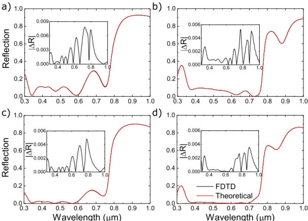
3.3.1 Reflection Profiles
Initially, the total reflection and transmission profiles were calculated using the FDTD method, representing the numerical approximation to the theoretical results, and the transfer matrix method, obtained from the Fresnel equations for a 1D multistack, repre-senting the analytical solution. By comparing both these results it is possible to verify the
C H A P T E R 3 . R E S U LT S A N D D I S C U S S I O N
500 1000 1500 2000
0.0 0.5 1.0 1.5 2.0
500 1000 1500 2000
0.0 0.5 1.0 1.5 2.0 b) I r r a d i a n c e ( W / m 2 n m )
W avelength (nm) AM1.5G
C
= 300, = 310 nm
C
= 400, = 310 nm
Change in absorption Power increase a)
W avelength (nm) AM1.5G
C
= 300, = 205 nm
C
= 300, = 400 nm
Absorption
Peak change from
higher
Figure 3.2: Resulting irradiance plots of the DS process used to simulate the effect of a
LDS layer. a) AM1.5G spectrum, in black, and 2 examples of resulting spectrums when the ∆λ remains constant as 310 nm and λ
C changes from 300 nm to 400 nm, in red
and blue, respectively, b) AM1.5G spectrum, in black, and 2 examples of the resulting spectrums whenλC remains constant at 300 nm and∆λvaries from 205 nm to 400 nm,
in red and blue, respectively.
accuracy of these numerical results.
Reflection profiles have 2 main components, specular reflection, Rs, and difuse
reflec-tion, Rd. The method used for these results calculates the total reflection meaning both
components are considered. However, because the results shown here are for PCs, there is no Rp, and thus the profiles for the PCs only have a specular component.
The reflection profiles for the 4 simulated PCs are shown in Figure 3.3. The equivalent transmission results are included in Annex III. From these plots, one can clearly see that the numerical simulation results make an excellent fit to theoretical curves over the entire simulation bandwidth. The inset profiles show the difference between the reflection
values of the numerical simulation and theoretical results, validating the simulation method used as the difference is always inferior to 9×10⁻³.
Considering the optical information shown in these graphs, one notices immediately the high reflection for wavelengths above 700 nm. When the cell thickness is increased, this effect is attenuated, as shown in Figure 3.3 b) and d) by the small dip around 900 nm.
This effect results from Fabry Perot-like interference patterns arising from constructive
interference of the propagating light [70]. However, the reflection, for the most part is still significative, reaching values up to 80%. Consequently, there is a need to create mechanisms to trap light and improve these losses, as will be further expanded later.
On the other side of the spectrum, under 700 nm, one can see the considerable low reflection, mainly attributed to the use of ITO as an anti-reflection coating. From Fresnel’s equations it is known that smaller differences in material’s refractive index, on an
inter-face, leads to lower reflection. Considering ITO’s index of 1.9, together with perovskite
3 . 3 . P L A N A R P E R OVS K I T E S O L A R C E L L S
0.3 0.4 0.5 0.6 0.7 0.8 0.9 1.0
0.0 0.2 0.4 0.6 0.8 1.0
0.3 0.4 0.5 0.6 0.7 0.8 0.9 1.0
0.0 0.2 0.4 0.6 0.8 1.0
0.3 0.4 0.5 0.6 0.7 0.8 0.9 1.0
0.0 0.2 0.4 0.6 0.8 1.0
0.3 0.4 0.5 0.6 0.7 0.8 0.9 1.0
0.0 0.2 0.4 0.6 0.8 1.0 R e f l e c t i o n FDT D T heoretical
0.4 0.6 0.8 1.0 0.000 0.003 0.006 0.009 R | d) c) b) a)
0.4 0.6 0.8 1.0 0.000 0.002 0.004 0.006 R | R e f l e c t i o n
W avelength ( m)
0.4 0.6 0.8 1.0 0.000 0.002 0.004 0.006 | R |
W avelength ( m)
0.4 0.6 0.8 1.0 0.000 0.002 0.004 0.006 | R |
Figure 3.3: Reflection profiles with the results from the numerical simulation, in black, and the results from the theoretical simulation, in red. Inset is represented the modulus of the difference between the two methods. a) PC with 250 nm perovskite, b) PC with
500 nm perovskite, c) PC with background index of 1.5 and 250 nm perovskite, d) PC with background index of 1.5 and 500 nm perovskite.
or TiO2’s index of 2.5 (under 700 nm) [80], a lower reflection would indeed be expected,
when compared with the vacuum index. This optical matching effect also explains the
difference between the reflection under 700 nm for the VBI case (Figure 3.3 a) and b)) and
the PBI case (Figure 3.3 c) and d)), since the latter provides a smaller index difference,
when compared to ITO. In fact, due to the similar refractive index of the background and ITO, there are some points where the observed reflection is nearing 0% (ideal matching case).
3.3.2 Absorption Profiles
The absorption profiles were calculated as described in Section 3.1, by integrating the absorbed power per unit volume, and are displayed in Figure 3.4. These plots have 4 main components: the absorption due to the perovskite layer, curve in black; the TiO2
layer, represented by the red shaded part; the remaining materials in the cell (ITO and Spiro), illustrated by the green shaded part. The last components are the inset profiles showing the absorbed power density throughout the cell for specific wavelengths, namely 350 and 900 nm. The first component is of paramount importance, as it represents the
C H A P T E R 3 . R E S U LT S A N D D I S C U S S I O N
absorption that will lead to the production of energy. The second component, due to TiO2being the main UV absorber in the cell, will also be very important to analyze the
optical gains from the shifted spectrum. The third simply represents the general parasitic absorption. However, it should be noted that ITO also has parasitic absorption leading to photocurrent gains. The last component, the inset profiles, exhibit the absorption behavior for different wavelengths.
Because the transmition values, shown in Annex III, are negligeable, the absorption can be calculated from the reflection using A = 1−R, where R is the reflection from
the previous subsection, meaning that both these parameters are intimately related. For most of the simulation bandwidth the 500 nm cells – Figure 3.4 b) and d) – show higher absorption than its 250 nm counterpart – Figure 3.4 a) and c) – since in the former light will have a higher travel path. In the last subsection it was discussed that the PBI cells’ reflection for wavelengths under 700 nm lowered around 10%, when compared with the VBI cells. This effect is also enhanced in these plots where the cell has better index
matching. Also present in these graphs is the lower absorption for wavelengths above 800 nm, that will be further analyzed in a later section, when the LTCs are introduced.
A relevant aspect present is the TiO2’s parasitic UV absorption - reaching values
between 10-20% under 400 nm - where the TiO2 is optically active. Despite the TiO2
reduced thickness, these values are still significant and impact perovskite’s absorption in these wavelengths. As will be shown in a later section, the increase in TiO2thickness
will lead to a further decrease in perovskite absorption due to higher absorption of this material, completely blocking the UV radiation from reaching the absorber.
For the remaining materials, in the most energetic section of the spectrum, the ab-sorption is mainly attributed to the ITO layer, as it is the first one in the cell, reaching values up to 20%. These absorption figures are corroborated by the inset profiles with the absorbed power for 350 nm, where it can be seen that Spiro’s absorption is almost negli-gible, being ITO and TiO2the second higher absorbers, after perovskite. Consequently,
it is expected that, with the use of a LDS material to change the incident spectrum, one will be able to mitigate the unwanted electron generation in these layers, shifting the photo-generation to the absorber layer.
For higher wavelength photons, there is parasitic absorption from both Spiro and ITO. From the inset profiles on the right, that show the absorbed power for 900 nm, one can see that these materials can reach similar absorption values to those of perovskite. Although this study is not the main focus of this work, it is also important to note that by reducing these parasitic absorptions and, therefore, increasing perovskite’s absorption, one can increase the cell’s Jph, as shown in recent works by Mendes et.al. [70, 71]. From
the standard AM 1.5G spectrum, shown in Section 3.2, it can be seen that there is still some relevant radiation for wavelengths above 800 nm.
Considering the absorption values above 80% for wavelengths ranging from 400 to 750 nm, the excellent absorption properties of perovskite are seen. Several equivalent studies, for amorphous silicon (a-Si) solar cells [70, 74], crystalline silicon cells [70], CIGS
3 . 3 . P L A N A R P E R OVS K I T E S O L A R C E L L S
cells [64] and even GaAs cells [68], show lower absorption for an equivalent wavelength range, when compared with perovskite’s. These outstanding absorption properties make perovskite a very compelling material for solar cells and this is, to some extent, part of the reason they are so widely studied.
Perovskite + T iO 2 Perovskite a) A b s o r p t i o n
Wavelength ( m)
-0.2-0.10.0 0.1 0.2
0.1 0.2 0.3 0.4 0.5 z ( m )
x (m)
1.0x10 -2 1.4x10 0 1.9x10 2 7.0x10 3 P abs (x10 16 cm -3 ) ITO TiO 2 Perovskite Spiro
-0.2-0.10.0 0.1 0.2
0.2 0.4 0.6 0.8 z ( m )
x ( m)
1.0x10 -4 6.7x10 -2 4.4x10 1 5.0x10 3 P abs (x10 16 cm -3 ) ITO TiO 2 Perovskite Spiro
-0.2-0.10.0 0.1 0.2 0.2 0.4 0.6 0.8 z ( m )
x (m)
1.0x10 -4 8.6x10 -2 7.4x10 1 1.0x10 4 P abs (x10 16 cm -3 ) ITO TiO 2 Perovskite Spiro
Wavelength ( m)
Figure 3.4: Absorption profiles with the absorption on the perovskite layer, in black; the TiO2 layer, in red; and the total cell absorption, in green. The inset profiles show the
plots for the absorbed power density through the cell volume for specific wavelengths, indicated by the arrows. The leftmost graph is the absorbed power for 350 nm and the rightmost graph is the absorbed power for 900 nm. a) and b) PC with VBI for 250 nm and 500 nm perovskite, respectively; c) and d) PC with PBI for 250 nm and 500 nm perovskite, respectively.
3.3.3 Photocurrent Shifts
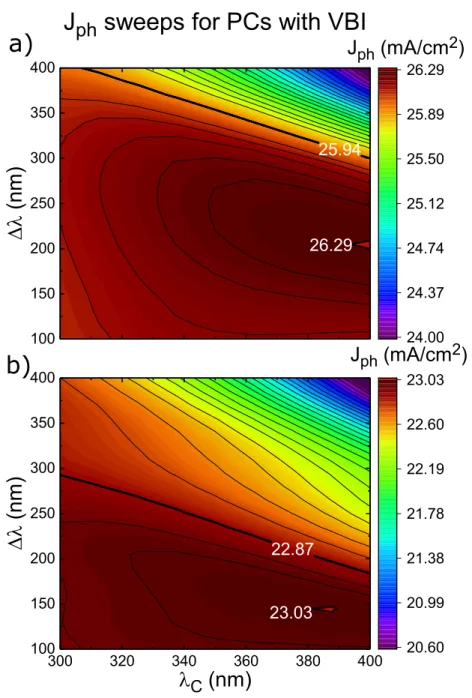
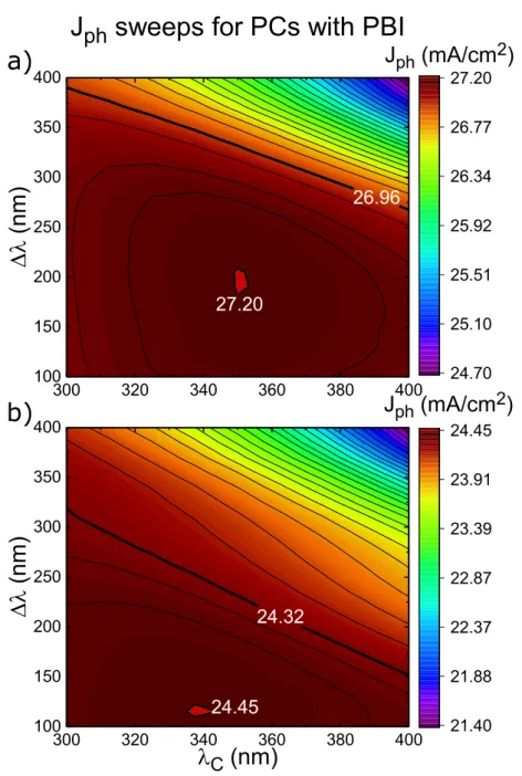
Together with the solar spectrum, the calculated absorption profiles, can be employed to obtain the maximum value of photocurrent in the cell, as described in Section 3.1. These values act as a figure of merit of the optical performance of the cell and, therefore can be used to compare different cell architectures.
By integrating different spectrums, using the process shown earlier in Figure 3.1, one
can emulate the effect on Jph of having an LDS material on top of the cell. Consequently,
a sweep was made, whereλC was varied between 300 and 400 nm and∆λbetween 100
C H A P T E R 3 . R E S U LT S A N D D I S C U S S I O N
25.94 26.29
22.87 23.03
100 150 200 250 300 350 400
(
n
m
)
24.00 24.37 24.74 25.12 25.50 25.89 26.29 J
ph
(mA/cm 2
)
300 320 340 360 380 400
100 150 200 250 300 350 400
b)
C
(nm)
(
n
m
)
20.60 20.99 21.38 21.78 22.19 22.60 23.03 J
ph
(mA/cm 2
)
a) J
ph
sweeps for PCs with VBI
Figure 3.5: Contour plots for the sweeps where λC and∆λ were varied from 300 nm
to 400 nm and 100 nm to 400 nm, respectively. a) PC with VBI for 500 nm perovskite layer and b) PC with VBI for 250 nm perovskite layer. The thicker line represents the contour corresponding to the photocurrent value obtained for the pristine spectrum. The indicated values represent the respective contour photocurrent value. The topmost value refers to the contour representing the pristine value, while the bottommost refers to the highest value contour in the plot.
3 . 3 . P L A N A R P E R OVS K I T E S O L A R C E L L S
26.96 27.20
24.32 24.45
300 320 340 360 380 400
100 150 200 250 300 350 400
a)
(
n
m
)
24.70 25.10 25.51 25.92 26.34 26.77 27.20 J
ph
(mA/cm 2
)
b)
300 320 340 360 380 400
100 150 200 250 300 350 400
J
ph
sweeps for PCs with PBI
C
(nm)
(
n
m
)
21.40 21.88 22.37 22.87 23.39 23.91 24.45 J
ph
(mA/cm 2
)
Figure 3.6: Contour plots for the sweeps whereλC and∆λ were varied from 300 nm
to 400 nm and 100 nm to 400 nm, respectively. a) PC with PBI for 500 nm perovskite layer, b) PC with PBI for 250 nm perovskite. The thicker line represents the contour cor-responding to the photocurrent value obtained for the pristine spectrum. The indicated values represent the respective contour photocurrent value. The topmost value refers to the contour representing the pristine value, while the bottommost refers to the highest value contour in the plot.
C H A P T E R 3 . R E S U LT S A N D D I S C U S S I O N
and 400 nm. The resulting plots are shown in Figure 3.5 for the VBI cell and in Figure 3.6 for PBI cell.
In all cases, the trend when both parameters change is similar and give a general idea of how the changing spectrum can influence the maximum current output. When con-sidering∆λabove 250 nm, J
phdrops steadily to a minimum, reaching values 2 mA/cm2
lower than the pristine value, shown by the thicker line in the different plots. The
absorp-tion profiles from the last secabsorp-tion show that, above 800 nm there is a significant reducabsorp-tion in the cell absorption, associated with the perovskite bandgap,∼1.55 eV, used for these simulations. Consequently, when the ∆λ is significantly increased, the spectrum gets
redshifted, Figure 3.1, to where the cell has lower performance negatively impacting its optical response.
In Table 3.1 the Jph for the pristine and optimized spectrums are summarized,
to-gether with their absolute and relative differences. Here it is seen that the differences are
small, with a maximum of 0.35 mA/cm2(1.3%) for the VBI cell with 500 nm perovskite.
The thin TiO2 layer used in these cells is the main factor inhibiting this increase as it
is the main UV absorber before perovskite. This lower parasitic absorption is optically advantageous, as it allows for an increase in perovskite’s absorption. However, practi-cally, it has some issues related with the UV degradation of MAPbI3. Several reports
have studied the degradation mechanisms, but the full picture hasn’t yet been totally understood. Nonetheless, one of the points of focus has been the creation of I2that leads
to the structural decomposition of perovskite’s crystal [55, 57]. This can appear at the TiO2/perovskite interface from TiO2’s catalytic effects [57] and from the known
photol-ysis of PbI2 present in the perovskite’s structure [55]. Therefore, on one side, the UV
shading of the cell produced by a thicker layer of TiO2could be seen as beneficial,
reduc-ing this degradation in detriment of the photocurrent that would be generated otherwise. However, considering TiO2’s photocatalytic effects under 400 nm the use of either a UV
filter or LDS are preferred to avoid perovskite’s degradation, with the latter enabling the reabsorption of the otherwise lost radiation [52].
The optimized∆λandλC values for the Jphfrom Table 3.1 are summarized in Table
3.2. Adding these values, the result varies between 400 to 500 nm, representing the wavelengths to where the spectrum is shifted. Given that these values depend heavily on the device absorption, which is more prevalent in the 400-700 nm range (Figure 3.4), these results were expected.
3.3.4 Generation Profiles and UV absorption
The generation profiles were calculated, as explained in Section 3.1, for the pristine spectrum and the one corresponding to the optimized∆λandλ
C values, shown in Section
3.3.3. The results for the PCs with VBI are shown in Figure 3.7 and, for the cells with PBI, in Figure 3.8. For all cases in study, the main difference is the reduction of the harmful
photo-generation in the TiO2 layer. This value varied from around 2×1026cm−3s−1to
3 . 3 . P L A N A R P E R OVS K I T E S O L A R C E L L S
Table 3.1: Summary of the optimized results obtained for the different PCs simulated.
AM1.5G Jphrepresents the values obtained in the pristine case and Shifted Jph represents
the optimized values resulting from the sweeps for each individual case. It is also shown the absolute and relative difference between the two.
Background refractive index 1 1.5
Perovskite thickness (nm) 250 500 250 500
AM1.5G Jph(mA/cm2) 22.87 25.94 24.32 26.96
Shifted Jph (mA/cm2) 23.03 26.29 24.45 27.20
∆Jph(mA/cm2) 0.16 0.35 0.13 0.24
∆Jph (%) 0.7 1.3 0.5 0.9
Table 3.2:∆λandλC values corresponding to the optimized values of Jphobtained from
the sweeps.
Background refractive index Perovskite thickness (nm) λC(nm) ∆λ(nm)
1 250 387.5 145
500 400.0 205
1.5 250 337.5 115
500 350.0 205
1×1026cm−3s−1for both 250 and 500 nm cells with VBI, and from around 3×1026cm−3s−1
to 0.2×1026cm−3s−1for the PBI case. Thus, the photo-generation changes to 50% and 7%
of the original value, deriving from the lower UV radiation irradiated onto the cell. As a result of the TiO2’s reduced absorption, an increase in the perovskite’s
photo-generation is observed as indicated in Figure 3.7 and 3.8. Equivalently, an increase in Spiro’s parasitic absorption was also obtained. One can attribute this latter addition to the increase in higher wavelength radiation, which has a higher penetration depth on the cell.
Perovskite’s UV absorption was considered by calculating Jphfor wavelengths between
300 nm and 400 nm, because, as was explained earlier, this parameter is intimately related with the solar cell’s absorption. For the PC with 250 nm and VBI, these values were 1.00 mA/cm2, with the pristine spectrum, and 0.15 mA/cm2, with the optimized spectrum. In
the 500 nm perovskite layer case, the same values were 1.00 mA/cm2and 0.20 mA/cm2.
Considering now the PBI cases, one obtained for the 250 nm cell 1.17 mA/cm2and 0.27 mA/cm2for the optimized and pristine spectrums, respectively, and, for the 500 nm cell,
1.09 mA/cm2and 0.16 mA/cm2. The corresponding percentual differences range from
75-85%, suggesting a significant reduction in the material UV absorption.
From these results, it can be inferred that either the TiO2’s photoactivity and
per-ovskite’s degradation under UV radiation would be reduced, even when one takes into account the non-ideal DS effects here suppressed, allowing these cells to maintain their
C H A P T E R 3 . R E S U LT S A N D D I S C U S S I O N
performance figures for a longer time period. Later, this point will be further expanded for the LTC. It can also be added that a small reduction in the ITO layer photo-generation was also achieved.
-0.2 -0.1 0.0 0.1 0.2
0.1 0.2 0.3 0.4 0.5 d) z ( m ) IT O T iO 2 Perov skite Spiro
-0.2 -0.1 0.0 0.1 0.2
c) b) 0.8 1.9 4.6 11.0 26.2 62.7 150.0 Generation (x10 26 cm -3 s -1 ) a)
-0.2 -0.1 0.0 0.1 0.2
0.15 0.30 0.45 0.60 0.75 Spiro Perov skite T iO 2 IT O z ( m )
x ( m )
-0.2 -0.1 0.0 0.1 0.2
x ( m )
0.8 1.9 4.6 11.0 26.2 62.7 150.0
Figure 3.7: Generation profiles for the PCs with VBI. a) cell with 250 nm perovskite; b) cell with 250 nm perovskite and optimized spectrum; c) cell with 500 nm perovskite; d) cell with 500 nm perovskite and optimized spectrum. The arrows and ellipse mark the biggest changes in the plots.
3.4 Solar Cells with Dielectric Photonic Structures
In this section, the focus is in the cells with photonic structures. As stated earlier, PC performance suffers from significant losses associated with lower absorption for higher
wavelengths, paving the way for the development of different methods to mitigate these
losses.
In this work, high dielectric constant structures are considered for use on top of solar cells to act as forward scatterers of light, causing an increase of its travel path, and, consequently, their chance of being absorbed [72, 74]. The use of these structures can also lead to the creation of localized modes in the absorber material that will then increase
3 . 4 . S O L A R C E L L S W I T H D I E L E C T R I C P H O TO N I C S T R U C T U R E S
-0.2 -0.1 0.0 0.1 0.2
0.1 0.2 0.3 0.4 0.5 z ( m ) IT O T iO 2 Perov skite Spiro
-0.2 -0.1 0.0 0.1 0.2
0.1 0.3 1.1 3.9 13.1 44.3 150.0 Generation (x10 26 cm -3 s -1 )
-0.2 -0.1 0.0 0.1 0.2
0.15 0.30 0.45 0.60 0.75 z ( m )
x ( m)
IT O
T iO 2
Perov skite
Spiro
-0.2 -0.1 0.0 0.1 0.2
c) d)
b)
x ( m)
0.2 0.6 1.8 5.5 16.5 49.8 150.0 a)
Figure 3.8: Generation profiles for the PCs with PBI. a) cell with 250 nm perovskite; b) cell with 250 nm perovskite and optimized spectrum; c) cell with 500 nm perovskite; d) cell with 500 nm perovskite and optimized spectrum. The arrows and ellipse mark the biggest changes in the plots.
the absorption due to the high intensity electric fields generated [72].
For this method, the format of the structures is rather important given that, according to the Fresnel’s equations, the reflection increases for steeper refractive index changes. As a result, various studies were conducted, where different structures were tested to
assess which one had the best optical performance [71]. The material used for these structures was TiO2, because of its low parasitic absorption for wavelengths above 400
nm and its high dielectric constant (around 2.5) [70]. The use of this material in silicon solar cells does not result in any significant photocurrent losses as, in TiO2photoactive
zone, silicon has a low absorption so TiO2’s parasitic absorption does not impact the cell
performance. However, when considering perovskite, the degrading effects of TiO2’s
photoactivity should be taken into account. As such, part of this section is centered in the effects of using an LDS material to minimize the absorption in the TiO2layer, that, in
practice, should result in a lower degradation of the perovskite material.