Diogo Farias Gonçalves Alexandre Rodrigues
Licenciado em Ciências da Engenharia
Plasma Nitriding of AA2011 Alloy and
Surface Characterization by NDT Techniques
Dissertação para obtenção do Grau de Mestre em
Engenharia Mecânica
Orientador: Doutor Telmo Santos, Professor Auxiliar,
Universidade Nova de Lisboa
Co-orientadores: Doutora Rosa Miranda, Professora Associada com Agregação,
Universidade Nova de Lisboa
Doutor Tatsuhiko Aizawa,
Shibaura Institute of Technology, Tóquio
i Plasma Nitriding of AA2011 Alloy and Surface Characterization by NDT Techniques
Copyright © 2015 Diogo Farias Gonçalves Alexandre Rodrigues
Faculdade Ciências e Tecnologia, Universidade Nova de Lisboa
iii Gostaria de agradecer ao meu orientador, o Prof. Telmo Santos, por me aceitar como orientando, por partilhar os seus conhecimentos na área dos ensaios não-destrutivos mas sobretudo por me motivar durante estes seis meses de investigação. Gostaria também de agradecer à minha co-orientadora, a Prof.ª Rosa Miranda, por ter sempre tempo para me ajudar, mesmo à distância, e por ter revisto a minha tese tantas vezes.
Não esquecendo os meus mentores e colegas do Japão, um muito obrigado ao Prof.Aizawa, ao Morita-san, ao Edo Yunata e ao Kurozumi-san por me terem acolhido em Tóquio e por me terem ensinado tudo o que sei sobre processos plasma.
Obrigado ao Patrick Inácio que, apesar de nos conhecermos pouco, perdeu quatro dias a fazer ensaios de condutividade só para mim.
Um obrigado e um beijinho à Carolina que teve força e paciência para esperar por mim. Um grande, grande obrigado à minha mãe que esteve comigo todos os dias, apesar de estar a 11.151 quilómetros de distância.
v I would like to thank my advisor, Prof. Telmo Santos, for taking me as his advisee, for sharing his knowledge in the field of non-destructive testing, but above all for keeping me motivated during these six months of research. I would also like to thank my co-advisor, Prof. Rosa Miranda, for always taking the time to help me and for revising my thesis so many times.
Not forgetting my mentors and colleagues in Japan I must send a word of thanks to Prof.Aizawa, Morita-san, Edo Yunata and Kurozumi-san. Thank you for receiving me with open arms and for teaching me everything I know about plasma treatments.
Thank you, Patrick Inácio, for taking four days to do conductivity tests with me, even though we do not know each other well.
A thank you and a kiss to Carolina for having the strength and the patience to wait for me. The biggest thank you to my mother for having been with me everyday, even though she was 11.151 kilometers away.
vii As ligas Al-Cu são frequentemente utilizadas nas industrias aeroespacial e automóvel pois possuem elevada resistência específica, especialmente em algumas condições de tratamento térmico. Contudo, devido a problemas de corrosão e desgaste, são normalmente anodizadas e pintadas. A nitruração por plasma foi proposta como alternativa, ainda que atualmente se encontre num estado pouco avançado de desenvolvimento para as ligas de Al.
As técnicas de caracterização elétrica estão bem implementadas na indústria enquanto técnicas de NDT devido à sua boa precisão associada a um baixo custo, relativamente a outros ensaios não-destrutivos. Algumas destas técnicas, como as correntes induzidas e as sondas de 4 pontos, são regularmente utilizadas em inspeções de revestimentos superficiais.
Esta tese teve como objectivo fazer nitruração por plasma a baixa temperatura de alumínio de modo a reduzir o impacto no tratamento de revenido inicial, bem como, estudar a possibilidade de utilização de correntes induzidas na caracterização das superfícies nitruradas.
O trabalho de investigação foi feito em duas fases. A primeira consistiu na calibração do processo e foi feita no Shibaura Institute of Technology, em Tóquio. A segunda consistiu na caracterização elétrica das amostras e foi feita no laboratório de ensaios não destrutivos, na Faculdade de Ciências e Tecnologia da UNL.
ix
ABSTRACT
Al-Cu alloys are widely used in the aerospace and automotive industries due to their high specific strength in some tempered conditions. However, due to poor corrosion and wear resistance, they are often anodized and/or painted. Plasma nitriding has been proposed as an alternative, though the developments in this technique are still in a recent stage for Al alloys.
Electrical characterization techniques are well implemented NDTs in the industry because of good accuracy associated with lower cost, compared to other methods. Some, like eddy currents and 4-point probe techniques, are often used in coating inspection.
The objective of this study was to perform Al nitriding at low temperatures to minimize the tempering initial condition damage and to assess the feasibility of eddy currents technique as a method for evaluating surface properties.
The work developed can be divided in two stages. The first one was the process tuning, done at the Shibaura Institute of Technology, in Tokyo; and the second was the electrical characterization done in Faculdade de Ciências e Tecnologia, UNL.
Low temperature nitriding of AA2011 alloy specimens was successfully achieved. Electrical conductivity results show that lift-off measurements by eddy currents testing can be related to surface properties.
KEY WORDS
xi
CONTENTS
AGRADECIMENTOS ... iii
ACKNOLEDGEMENTS ... v
RESUMO ... vii
ABSTRACT ... ix
LIST OF FIGURES ...xiii
LIST OF TABLES ... xv
1. INTRODUCTION ... 1
1.1. Motivation... 1
1.2. Objective ... 2
1.3. Thesis Structure ... 2
2. NITRIDING OF ALUMINUM ALLOYS ... 3
2.1. Aluminum and its alloys ... 3
2.1.1. Precipitation Hardening ... 4
2.2. Corrosion Resistance ... 8
2.3. Nitriding ... 8
2.4. Plasma Nitriding ... 11
2.4.1. Plasma Generation ... 11
2.4.2. Process parameters ... 14
2.5. AlN and its formation ... 16
2.6. Characterization of Nitrided Surfaces ... 18
2.7. Summary ... 18
3. ELECTRICAL CHARACTERIZATION ... 19
3.1. Characterization by Eddy Currents ... 19
4. EXPERIMENTAL PROCEDURE ... 23
4.1. Materials ... 23
xii
4.3. Parameters ... 25
4.3.1. Cathode Configurations ... 28
4.3.2. Cover for Electrical Conductivity Tests ... 30
4.3.3. Temperature Measurements ... 30
4.4. Testing ... 31
4.4.1. SEM ... 31
4.4.2. Electrical conductivity ... 31
4.4.3. Hardness measurements ... 33
5. RESULTS AND DISCUSSIONS ... 35
5.1. Process tuning ... 35
5.1.1. Hot processed samples ... 35
5.1.2. Cold processed samples ... 37
5.2. Effects of cathode configuration and DC bias on temperature ... 42
5.3. SEM ... 48
5.4. Electrical Characterization ... 51
5.5. Vickers Microindentation Hardness Tests ... 56
6. FINAL CONCLUSIONS ... 59
xiii
LIST OF FIGURES
FIG.1–ALUMINUM RICH SECTION OF THE AL-CU PHASE DIAGRAM.[1] ... 5
FIG.2–EFFECTS OF AGING TIME IN MICROSTRUCTURE AND YIELD STRENGTH OF LOW COPPER AL-CU ALLOYS. ... 6
FIG.3–AL-CU PHASE DIAGRAM SHOWING TEMPERATURE RANGES FOR SOLUTION HEAT TREATING, ANNEALING AND PRECIPITATION HARDENING.[2] ... 7
FIG.4–RELATIONSHIP BETWEEN RESULTING YIELD STRENGTH, HOLDING TIME AND TEMPERATURE IN ARTIFICIAL AGING OF A 2024 ALLOY.[2] ... 7
FIG.5–SCHEMATIC EXAMPLE OF DC PLASMA EQUIPMENT [7].1) SAMPLE;2) DUMMY SAMPLE;3) TABLE;4) HEATER;5) CATHODE;6) INSULATOR;7) THERMOCOUPLE;8)/9) GAS INLETS;10) TO PUMP;11) AMP.METER;12)VOLT METER;13) DC POWER SUPPLY. ... 13
FIG.6–SCHEMATIC EXAMPLE OF RADIO FREQUENCY PLASMA NITRIDING EQUIPMENT [5]. ... 13
FIG.7–NITRIDE LAYER THICKNESS HAS FUNCTION OF NITRIDING TIME FOR AL 1100[9]. ... 15
FIG.8–VARIATION OF SURFACE HARDNESS WITH TESTING LOAD.SAMPLE IS AA2011 NITRIDED WITH HDPN.[11] ... 15
FIG.9-𝐴𝑙𝑁 WURTZITE STRUCTURE WITH LATTICE CONSTANTS 𝑎 = 3.11Å AND 𝑏 = 4.98Å[3]. ... 16
FIG.10–ALN FORMATION ON THE SURFACE OF PURE ALUMINUM IN NITROGEN-HYDROGEN ATMOSPHERE [7]. ... 17
FIG.11ELECTROMAGNETIC INDUCTION IN EDDY CURRENTS TESTING.PRIMARY MAGNETIC FIELD (BLUE), GENERATED BY AC CURRENT CIRCULATING IN THE COIL, INDUCES AN AC CURRENT (RED) IN THE INSPECTED PART.THIS CURRENT CREATES A SECONDARY MAGNETIC FIELD (YELLOW) THAT OPPOSES THE PRIMARY FIELD. ... 20
FIG.12–EDDY CURRENT IMPEDANCE RESPONSE PLANE [22](ADAPTED) ... 21
FIG.13– A)TYPE 0 SAMPLE MIRROR LIKE-SURFACE WITH SHARP, AS-CUT EDGES; B)TYPE 1 SAMPLE POLISHED WITH SANDPAPER AND BEVELED EDGES ... 23
FIG.14–NITRIDING EQUIPMENT:1) VACUUM CHAMBER;2) VACUUM PUMPS;3)RF POWER SUPPLY;4)DC BIAS POWER SUPPLY; 5)PLC CONTROLLER;6) COOLING UNIT;7) GAS FEED LINES;8) POWER UNIT. ... 24
FIG.15–INTERIOR OF THE VACUUM CHAMBER.1)RF ELECTRODES,2) THERMOCOUPLE,3) HEATER PLATE AND 4) GAS FEED (TUBE NOT PICTURED). ... 25
FIG.16–CATHODE CONFIGURATIONS USED IN HOT AND COLD PROCESSED EXPERIMENTS.SAMPLES PLACED ON THE INSIDE OF THE HOLLOW TUBE.RED ARROW INDICATES THE POSITION OF THE GAS FEED TUBE. ... 29
FIG.17–SAMPLES COVERED WITH A) A THIN STEEL DISC AND B) A THICK ALUMINUM DISC, TO OBTAIN AN NON NITRIDED AREA FOR REFERENCE DURING THE ELECTRICAL CONDUCTIVITY MEASUREMENTS. ... 30
FIG.18– A)LOCATION OF THERMOCOUPLE FOR SAMPLE T1 AND T2; B)LOCATION OF THERMOCOUPLE FOR SAMPLES T13 AND T14 ... 31
FIG.19–EDDY CURRENTS TEST POSITIONING SYSTEM. ... 32
FIG.20–SAMPLE H3 AFTER PROCESSING (A) AND RESPECTIVE CATHODE CONFIGURATION (B). ... 35
FIG.21–SAMPLES A)H1, NITRIDED WITH CATHODE CONFIGURATION A); AND B)H2, NITRIDED WITH CATHODE CONFIGURATION C). BOTH EXHIBIT EXCESSIVE NITRIDE DEPOSITION AND SEVERE DELAMINATION. ... 36
FIG.22–SAMPLES H91,H92 AND H93 AFTER PROCESSING (A, B AND C) AND RESPECTIVE CATHODE CONFIGURATION (D). ... 37
FIG.23–A)SAMPLE H6 AFTER NITRIDING AT 100℃ FOR 3600 S(1 H) AND B) RESPECTIVE CATHODE CONFIGURATION (NARROW CYLINDER). ... 38
FIG.24– A)SAMPLE C3 AFTER NITRIDING AT AROUND 100℃ FOR 3600 S(1 H); B) RESPECTIVE CATHODE CONFIGURATION (WIDE CYLINDER). ... 38
xiv
FIG.26-SAMPLE C32 AFTER NITRIDING FOR 10800 S(3 H), AT 300V, STARTING AT 86℃. ... 39
FIG.27-SAMPLE C49 AFTER NITRIDING FOR 18000 S (5 H) AT 470V, STARTING AT 196℃, WITHOUT HEATING DURING THE PROCESS; RESPECTIVE CATHODE CONFIGURATION. ... 39
FIG.28– A)C51 WITH 470VDC BIAS; B)C52 WITH 400VDC BIAS; C)C5 WITH 300VDC BIAS.ALL NITRIDED FOR 14400 S(4 H), STARTING AT 86 ℃, WITHOUT HEATING DURING THE PROCESS. ... 40
FIG.29–SAMPLES B2 AND B3 AFTER NITRIDING FOR 14400 S (4 H), AT 470V, STARTING AT 150℃ AND 180℃, RESPECTIVELY. ... 40
FIG.30– A) SAMPLE B31(450VDC BIAS); B) SAMPLE B34(460VDC BIAS); BOTH NITRIDED FOR 18000 S (5 H) AT 180℃. 41 FIG.31–SAMPLES A)A1, PLACED AT THE ENTRANCE OF THE HOLLOW CATHODE; AND B)A2, PLACED 34 LENGTH INSIDE THE HOLLOW CATHODE.BOTH PRE-HEATED TO 100℃ AND NITRIDED WITH 470VDC FOR 10800 S (3 H). D)CATHODE CONFIGURATION USED IN THESE EXPERIMENTS. ... 41
FIG.32–SAMPLES A)A3, PRE-HEATED TO 150℃; AND B)A4, CONSTANT TEMPERATURE OF 180℃.BOTH NITRIDED WITH 470V DC, FOR 14400S (4H) AND WITH CATHODE CONFIGURATION E) ... 42
FIG.33–TEMPERATURE MEASUREMENTS OF SAMPLES C32, NITRIDE WITH CATHODE CONFIG A), AND C32, NITRIDED WITH CATHODE CONFIG. B).THERMOCOUPLE ON THE HEATER PLATE. ... 43
FIG.34–TEMPERATURE MEASUREMENTS OF SAMPLES B1(PRE-HEATED TO 100℃),B2(PRE-HEATED TO 150℃) AND B3 (HEATED TO 180℃ THROUGHOUT).ALL NITRIDE WITH CATHODE CONFIG C) AND 470VDC BIAS.THERMOCOUPLE ON THE HEATER PLATE. ... 44
FIG.35-TEMPERATURE MEASUREMENTS OF SAMPLES A2(PRE-HEATED TO 100℃),A3(PRE-HEATED TO 150℃) AND A4 (HEATED TO 180℃ THROUGHOUT).ALL NITRIDE WITH CATHODE CONFIG E) AND 470VDC BIAS.THERMOCOUPLE ON THE HEATER PLATE. ... 44
FIG.36–TEMPERATURES MEASURED ON THE HEATER PLATE, USING C) AND D) CATHODE CONFIGURATIONS WITH 300VDC BIAS(SAMPLES T1 AND T21, RESPECTIVELY) ... 45
FIG.37–TEMPERATURES MEASURED AT THE SURFACE OF THE SAMPLE WITH LONGITUDINAL (L) AND TRANSVERSE (T) HOLLOW CATHODE CONFIGURATIONS AT 300VDC BIAS. ... 46
FIG.38-TEMPERATURES ON THE SURFACE OF THE SAMPLE (300V), ON THE SUBSTRATE (470V) AND ON THE HEATER PLATE (470 V), WITH THE TRANSVERSE C) HOLLOW CATHODE CONFIGURATION.SUBSTRATE TEMPERATURE WAS MEASURED WITH SAMPLE ON THE CEILING OF THE HOLLOW CATHODE. ... 47
FIG.39–SEM MICROGRAPH SHOWING THE EARLY STAGE OF 𝐴𝑙𝑁 FORMATION ON A MIRROR FINISHED SAMPLE AFTER PRE -SPUTTERING WITH 470V AT 400℃. ... 48
FIG.40–SEM MICROGRAPH SHOWING NITRIDE CLUSTER FORMATION. ... 49
FIG.41–SEM MICROGRAPH SHOWING A FULLY NITRIDED SURFACE. ... 49
FIG.42–SEM MICROGRAPHS SHOWING TWO NITRIDED SURFACES: A) STARTING FROM A POLISHED SURFACE, AND B) STARTING FROM AN UNPOLISHED, AS-CUT SURFACE. ... 51
FIG.43–EDDY CURRENT 3D PLOT OF SAMPLE H91;𝐼𝑚𝑧= LIFT-OFF. ... 52
FIG.44–EDDY CURRENT 3D PLOT OF SAMPLE H92;𝐼𝑚𝑧= LIFT-OFF. ... 53
FIG.45–EDDY CURRENT 3D PLOT OF SAMPLE H93;𝐼𝑚𝑧= LIFT-OFF. ... 54
FIG.46–LIFT-OFF AT 500 KHZ, OVERLAPPED WITH SAMPLE A)H91, B)H92, AND C)H93. ... 55
FIG.47–EDDY CURRENT 3D PLOT OF SAMPLES A)H91, B)H92 AND C)H93;𝑅𝑒𝑧= ELECTRICAL CONDUCTIVITY. ... 56
xv
LIST OF TABLES
TAB.1–SPUTTERING AND NITRIDING PARAMETERS OF HOT PROCESSED SAMPLES. ... 26
TAB.2–NITRIDING PARAMETERS COLD PROCESSED SAMPLES. ... 27
TAB.3–EDDY CURRENT PENETRATION DEPTH OF EACH AC CURRENT FREQUENCY ... 33
TAB.4–RESOLUTION OF EC TESTS. ... 33
1
1.
INTRODUCTION
1.1.
Motivation
Aluminum is a material with great potential for many industrial applications. It offers an interesting combination of properties in alloy form, such as light weight, high strength and good general workability. These characteristics make it attractive for use in fields such as aerospace, automotive, railway and marine. Aluminum increases its strength as temperature decreases, and thus it is suitable for cryogenic purposes such as in pressure vessels and space technology. It is resistant to corrosion due to the thin oxide film that forms on its surface after contact with air moist.
In spite of these attractive properties, aluminum has poor mechanical surface properties that lead to high wear and, in some alloys, to high corrosion. Surface enhancing technologies are standard in modern industries. Tribological properties of several metals can be improved by processes such as carburizing, nitriding, boriding, anodizing, chemical vapor deposition, electroplating, etc. Surface properties of aluminum are usually enhanced by anodizing though it produces some problems like high porosity and high wear. An alternative to anodizing is Nitriding. Nitriding forms a surface layer of aluminum nitride that has high hardness and high corrosion and wear resistances. Aluminum nitride has an advantage over aluminum oxide in marine applications because it passivates and does not dissolve by reaction with chloride. However, because aluminum nitriding is still fairly recent, process parameters and nitride formation mechanisms are still not entirely understood.
Chapter 1 - Introduction
2
This was a joint work between the Non-Destructive Testing (NDT) laboratory of the Department of Mechanical and Industrial Engineering of FCT and the Nano-Film and Coating (NFC) laboratory of the Department of Engineering and Design of the Shibaura Institute of Technology (SIT). The knowledge and equipment available at both the NDT and NFC laboratories made this work possible.
1.2.
Objective
This work aims to contribute to a further understanding of the plasma nitriding process, in order to make it significantly superior and reliable for industrial applications in aluminum alloys. In this specific case, nitriding of alloy AA2011 was studied, as well as the parameters that produce the most uniform and smooth coatings. Since most aluminum alloys are hardened and tempered, nitriding was performed at low temperature which was innovative for Al alloys.
The eddy currents technique is proposed as a non-destructive test to determine the characteristics of this type of diffusion coating. Ideally it will be able to describe the nitride layer in terms of thickness, concentration gradient and hardness.
1.3.
Thesis Structure
This thesis is structured in 6 chapters. The first contains the motivation and the objectives of the work. Chapter 2 describes the state-of-the-art in plasma nitriding of aluminum alloys, including the techniques employed and the current understanding of the nitriding mechanisms.
Chapter 3 presents the state-of-the-art in eddy currents testing, as well as the basics and fundamentals of the method.
In chapter 4, the materials, equipment and experimental procedure are described.
In chapter 5 the nitriding results are presented and discussed. This includes preliminary inspection of the nitrided samples, analysis of the conductivity and hardness tests and preliminary conclusions.
3
2.
NITRIDING OF ALUMINUM ALLOYS
This chapter provides an overview of the existing methods for improving surface performance of the 2xxx series alloys, in terms of surface hardness, corrosion and wear. A brief introduction to aluminum alloys is given, followed by a description of plasma nitriding principles and techniques.
2.1.
Aluminum and its alloys
Aluminum occurs near the Earth’s surface in deposits of bauxite, usually tightly combined
with oxygen and silicon. In Earth’s crust, it is the third most abundant element (8%), surpassed only by oxygen (47%) and silicon (28%), and the most abundant metal. The difficulty of extracting aluminum from its natural deposits raises its cost relatively to some less plentiful metals but its unique set of characteristics make attractive to many industries.
Chapter 2 – Nitriding of Aluminum Alloys
4
than 10% in total) of copper, magnesium, manganese, silicon, tin, zinc and others, to modify the properties of aluminum in a desired way, given that only some elements effectively increase the mechanical properties.
Aluminum alloys are divided into two classifications: casting alloys, those that are melted and poured into a mold; and wrought alloys, those that are worked mechanically in the solid state. Cast alloys contain higher percentages of alloying elements resulting in a more heterogeneous structure and, generally, lower ductility in comparison to wrought alloys. Wrought alloys are the most used in the aforementioned industries because of their higher melting point and tensile strength. Aluminum alloys increase their strength by cold working but only some have a significate response to heat treatments, therefore, they are subdivided into heat-treatable and non-heat-treatable.
2xxx
The 2xxx series are a heat treatable series in which copper is the primary alloying element, giving them high strength but little corrosion resistance. They were widely used in the aerospace industry but, because of weldability, machinability, wear and corrosion issues, they have been replaced by alloys of the 7xxx series in many applications. They are heat treatable because of their high copper content which makes them unsuitable for fusion welding processes. Solid state welding is the most adequate for these alloys and therefore welding is limited to certain part geometries and joint configurations.
2.1.1. Precipitation Hardening
5 Although most binary aluminum alloy systems form precipitates, not all of them have a significant response to heat treatments. The composition and concentration of the precipitates are the main factors that contribute to the strength of an alloy. The systems that respond better are the aluminum-copper, the aluminum-copper-magnesium, the aluminum-magnesium-silicon and the aluminum-zinc-magnesium-copper. In order to understand the basic principles of precipitation hardening, let us study the simpler of systems, the binary aluminum-copper system. Fig. 1 shows the Al-Cu phase diagram, typical of the 2xxx series alloys.
Fig. 1 – Aluminum rich section of the Al-Cu phase diagram. [1]
Chapter 2 – Nitriding of Aluminum Alloys
6
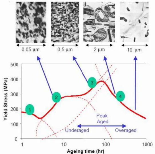
After quenching, the alloy will go through what is called aging or precipitation hardening, as in the example shown in Fig. 2. At a temperature well below the solvus line, in solute-rich regions designated Guinier-Preston (GP) zones, coherent 𝐴𝑙2𝐶𝑢 precipitates (𝜃′′) start to form initially lowering strength due to a lowering of the copper content of the matrix (1). Afterwards, as these coherent precipitates grow in the GP zones, strength increases (2). Intersections between precipitates and dislocations further increase hardness (3) until a peak is reached when incoherent 𝜃 precipitates start to form (4) and the alloy starts to anneal.
Fig. 2 – Effects of aging time in microstructure and yield strength of low copper Al-Cu alloys.
An aged alloy that has not yet reached its peak hardness is called underaged, while an alloy that has surpassed this peak is called overaged. Overaging will lead to partial or full annealing.
7 ranges for solution heat treatments, annealing and artificial aging in an aluminum copper system. Fig. 4 correlates the processing temperature and time with the resulting yield strength for an AA2024 alloy. Understanding aging is very important in alloy selection in order to take full advantage of the enhanced characteristics of the 2xxx series alloys.
Fig. 3 – Al-Cu phase diagram showing temperature ranges for solution heat treating, annealing and precipitation hardening. [2]
Chapter 2 – Nitriding of Aluminum Alloys
8
2.2.
Corrosion Resistance
Corrosion resistance is one of the most important properties of materials when it comes to determining the service life of a component. It depends on the composition of the material, and on the strength, electric current, temperature and environment to which a component is subjected to. Most aluminum alloys are less corrosion resistant than pure aluminum. General corrosion resistance is usually an inverse function of copper content and, therefore, the 2xxx series are the least corrosion resistant alongside some alloys of the 7xxx series. Other alloying elements like lead, nickel and tin also tend to decrease corrosion resistance though to a smaller extent.
Though the mechanisms involved at a microscopic level are the same, at a macroscopic level corrosion can manifest in different forms, such as galvanic corrosion, pitting corrosion, crevice corrosion and Stress Corrosion Cracking (SCC).
The 2xxx series alloys are more prone to corrosion because they contain copper, which precipitates in the form of Al-Cu particles, and some contain copper and magnesium, which precipitate in the form of Al-Cu-Mg particles. The area involving each of these is a propitious site for pit initiation because they are cathodic to the matrix (Al-Cu-Mg particles are initially anodic but they become cathodic due to dealloying). During dissolution of the Al-Cu(-Mg) particles, regions with metallic copper are formed in the matrix, thereby contributing to further galvanic corrosion and sustaining the pit growth. These precipitates also make the alloy more susceptible to intergranular corrosion (IG) and SCC, though this susceptibility can vary significantly with copper content and temper conditions. Slow quenching makes the alloy susceptible to IG corrosion, while rapid quenching makes more susceptible to SCC because of bigger precipitates.
2.3.
Nitriding
9 Nitrogen can be delivered to the surface of a component by three different donors: gas, salts and ions.
In gas nitriding, a nitrogen rich gas, usually ammonia (𝑁𝐻3), delivers nitrogen to the surface of a component. Inside a gas filled chamber, components are heated in order to supply energy to the ammonia molecules. These dissociate into hydrogen and nitrogen and the latter penetrates the surface to create a nitride layer. Gas nitriding is the oldest and simplest of the three and it has been used for almost a century on steel alloys.
In salt bath nitriding, components are heated and dipped in a tank filled with a bath containing cyanides or cyanates. It is a much simpler process than gas nitriding but has a narrower range of applications. Due to high toxicity of the salts it has been less used in the last decades in favor of cleaner technologies.
In ion nitriding, as the name suggests, nitrogen is delivered to the surface of a component in the form of ions generated in a plasma. In addition to a heat source to heat samples, it requires electronic control and electric power supply to generate and sustain the plasma. Nevertheless, in general, it has the lowest power consumption of the three. Unlike gas nitriding, it works with lower gas pressures and consequently has lower gas consumption. Unlike salt bath nitriding it does not utilize nor produce toxic substances.
In the case of aluminum, nitriding involves substituting the aluminum oxide (𝐴𝑙2𝑂3) layer for aluminum nitride (𝐴𝑙𝑁). Early attempts have lead to thickness irregularity, detachment and contamination of the nitride layer, mainly due to the presence of 𝐴𝑙2𝑂3 acting as a barrier between metal and nitrogen and retarding the diffusion of nitrogen into the substrate. Complete removal of the alumina layer before nitriding and absence of 𝑂2 during nitriding are paramount. As a result aluminum nitriding becomes a much more demanding process. There are several methods for removing the oxide layer: addition of magnesium, ball milling in a controlled atmosphere and sputtering.
Chapter 2 – Nitriding of Aluminum Alloys
10
Ion Nitriding
There are two main types of ion nitriding processes, Nitrogen Ion Implantation (NII) and Plasma Nitriding (PN), distinguishable by the main mechanism of ion introduction to produce case hardened layers.
Nitrogen Ion Implantation (NII) is a high energy, non-thermal, non-equilibrium, physically driven, ballistic alloying process. Concentrated in a beam, nitrogen ions accelerate towards the surface of a sample to bombard it with sufficient kinetic energy to produce a hardened layer. The layer is relatively shallow but very hard. The beam propagates in high vacuum at room temperature and is generated in an atomic particle accelerator. Surface hardening in mostly due to dislocation pinning.
Plasma Nitriding (PN), on the other hand, is a low energy, thermally driven, equilibrium, diffusion process. In a plasma created around a sample, nitrogen neutrals and ions react chemically with the surface atoms to create a nitride layer that grows by diffusion. The resulting layer is relatively deep but less hard than in NII. In PN the plasma usually has relatively low energy density and therefore components must be heated to facilitate the process. Surface hardening is mostly due to metal nitride precipitates [2].
11
2.4.
Plasma Nitriding
Plasma technology and equipment setups used for aluminum nitriding are similar to the ones used for nitriding of steel alloys, as well as for many other industrial plasma processes such as sputtering, Physical Vapor Deposition (PVD) and plasma etching. However, because the mechanism of 𝐴𝑙𝑁 formation and the influence of the many process parameters are not yet fully understood, this process is still in a very premature stage of development.
Many authors have reported to successfully nitride several aluminum alloys but all with different parameters and different results. For instance, a DC plasma study has reported a
10 μm thickness layer on an aluminum-titanium alloy [4] while another study that employed RF plasma reported a 4.5 nm thickness layer on a 2xxx series alloy [5], both with processing times in excess of 20 h. An ECR study reported a very high thickness of
10 μm for a processing time of just 900 s [6] though extensive fusion of the substrate occurred, which is not desirable, especially in the case of heat-treatable aluminum alloys like the 2xxx and 7xxx series.
For this work a High Density Plasma (HD-Plasma) system, recently developed at SIT, was used to combine the more conventional DC- and RF-Plasma systems in order to mitigate
each system’s flaws. In this chapter a general process description is presented, then DC-, RF- and HD-systems are explained as well as process parameters for each case.
2.4.1. Plasma Generation
Plasma is usually described as the fourth state-of-matter, with some similarities to the gas phase and also some differences. It is a neutral medium of unbound positive and negative particles that interact with each other collectively in waves. Plasma is the most common phase of matter in the universe, present in lightning and in the nuclei of stars; it can also be generated artificially, such as in neon lamps and arc welding.
Chapter 2 – Nitriding of Aluminum Alloys
12
gas (electrical insulator) ionizes transforming into plasma (excellent electric conductor) and producing a glowing light. This was the first method for producing artificial plasma and it is also known as glow discharge. It was the first low pressure discharge used to nitride aluminum [7] and , in the present work, it will be referred to as DC plasma.
Another way of generating artificial plasma is by supplying the gas with current produced by electromagnetic induction. This can be achieved by applying high radio frequency AC current on a coil placed outside the chamber that will create a time-varying magnetic field, which will in turns originate electric currents inside the chamber. This is called Radio Frequency Inductively Coupled Plasma (RFICP) and it has been used to successfully nitride
aluminum alloys using an equipment setup referred to here as RF Plasma.
Higher frequencies (high RF or Microwave) are also used to generate plasma in low-pressure discharges called Wave Heated Discharges. For example, Electron Cyclotron Resonance (ECR) uses a microwave source in combination with a permanent magnetic field in order to ionize gas. It is used in the biomedical industry and it has been applied in plasma nitriding of pure aluminum [6].
DC Plasma
13
Fig. 5 – Schematic example of DC plasma equipment [7]. 1) sample; 2) dummy sample; 3) table; 4) heater; 5) cathode; 6) insulator; 7) thermocouple; 8)/9) gas inlets; 10) to pump; 11) amp. Meter; 12) Volt meter; 13) DC power supply.
RF Plasma
Fig. 6, shows an example of an RF plasma apparatus. Here there is an inductive coil placed outside the chamber, responsible for plasma generation, a DC between the chamber and the workpiece that has the sole function of accelerating ions. This way the DC bias does not need to be as high, preventing the problems associated with DC plasma but producing very thin layers [5]. The use of hollow cathodes is frequent in this type of setup [8].
Chapter 2 – Nitriding of Aluminum Alloys
14
High Density Plasma Nitriding
High Density Plasma Nitriding (HDPN) is the name, given in recent articles, to methods that combine DC and RF plasma generation. By combining these two methods, it is possible to create energy collisions and to confine these collision to a specific region in the chamber. Understanding the magnetic fields involved in the process is essential to understanding this process, though currently there is little knowledge in this regard.
2.4.2. Process parameters
For the purpose of this work let us consider only the process parameters of a high density plasma machine. DC voltage, RF voltage, holding temperature, processing time, gas pressure and gas ratio should change according to composition and geometry of the part to be nitrided.
The influence of the many process parameters in the resulting nitrided workpiece is still trial based and not fully understood. Nonetheless, some conclusions have been drawn [5] [9]:
Higher gas pressure leads to higher nitrogen activity and density near the surface of the workpiece which, in turns, leads to higher 𝐴𝑙𝑁 formation rate;
Nitrogen-hydrogen mixture is the most suitable for nitriding as hydrogen acts as a catalyst, promoting 𝐴𝑙𝑁 formation. Mixture ratio depends on the aluminum alloy;
15
Fig. 7 – Nitride layer thickness has function of nitriding time for Al 1100 [9].
Surface roughness can be effectively controlled by varying applied DC voltage. Higher voltages produce rougher surfaces due to severe sputtering by ions with high kinetic energy. RF plasma produces smoother surfaces than DC plasma.
𝑁𝐻 radicals contained in the nitrogen-hydrogen plasma have been shown to react with 𝐴𝑙2𝐶𝑢 precipitates in cu-based alloys, acting as catalist for 𝐴𝑙𝑁 formation [10].
Previous research has demonstrated that surface hardening of Al-Cu alloys is possible by using HDPN equipment [11]. Fig. 8 shows hardness values for a nitrided AA2011 sample between 400 HV and 800 HV, with loads of 50 g (0.5 N) and 10 g (0.1 N), respectively.
Chapter 2 – Nitriding of Aluminum Alloys
16
2.5.
AlN and its formation
In equilibrium phase, aluminum nitride (𝐴𝑙𝑁) has a hexagonal close packed wurtzite structure, as shown in Fig. 9, with mass density equal to 3.26 g/cm3. It is thermally stable (melting temperature of 2490 ºC [12]), chemically stable, resistant to corrosion and very resistant to wear (1200 HV [13]). Alongside excellent tribological properties it has other interesting thermal, electrical, optical and acoustic properties. For temperatures of 25 ºC and 600 ºC, 𝐴𝑙𝑁 has a high thermal conductivity coefficient of 30.1 Wm−1K−1 and
20.1 Wm−1K−1, respectively, and small and relatively constant thermal expansion
coefficient of 4.84 × 10⁻⁶ K−1. It has a high specific electrical resistivity of 1013 Ω𝑚, it has piezoelectric properties and it is highly transparent for wavelengths from 200 𝑛𝑚 to
12.5 μm. Because of all these properties, 𝐴𝑙𝑁 has a variety of applications in many industries such as tooling, optoelectronics and telecommunications.
Fig. 9 - 𝐴𝑙𝑁 wurtzite structure with lattice constants 𝑎 = 3.11 Å and 𝑏 = 4.98 Å [3].
Formation mechanism of the nitride layer by plasma nitriding on an aluminum substrate is illustrated in Fig. 10.
During the pre-sputtering phase, considering the chamber contains only 𝑁2, many excited species form when the gas is ionized. The positive charged species are accelerated towards the cathode and, if the energy is sufficient (this usually happens with the heavier
𝑁2+ species), the collisions will break the 𝐴𝑙2𝑂3 layer. The oxide layer will not form again
17 conditions are not favorable because of the high mobility of the reactive species in the plasma.
In the nitriding phase, the excited nitrogen species either react with the 𝐴𝑙 atoms on the substrate, or with sputtered 𝐴𝑙 atoms and then deposit on the substrate. After this the nitrogen atoms migrate away from the surface, into the substrate. and form a layer with a negative concentration gradient, a functionally graded material. This creates very good adhesion and minimizes the problems associated with ceramic coating of metals, like cracking because of different thermal expansion coefficients. After coming into contact with air, 𝐴𝑙𝑁 reacts with air moisture creating a thin layer of aluminum hydroxide and giving the surface a darker color. The formation rate of 𝐴𝑙(𝑂𝐻3) is very slow and thus it protects 𝐴𝑙𝑁 from further oxidation.
Fig. 10 – AlN formation on the surface of pure aluminum in nitrogen-hydrogen atmosphere [7].
During the nitriding phase, if the 𝐴𝑙𝑁 formation rate is higher than the diffusion rate of nitrogen into aluminum, a very thick layer with bad substrate adhesion will form. Fick’s first law of diffusion gives the diffusive flux in mol m⁄ 2s as
𝐽 = −𝐷𝜕Φ𝜕𝑥 ;
where 𝐷 is the diffusion coeficient in m2⁄s, Φ is the concentration in mol m⁄ 3, and 𝑥 is the length in the direction of diffusion in m. As can be seen the flux decreases as the layer grows because the concentration gradient 𝜕Φ 𝜕𝑥⁄ will be progressively less negative. It is possible to control the diffusive flux by controlling the diffusion coefficient 𝐷 given by
Chapter 2 – Nitriding of Aluminum Alloys
18
where 𝐷0 is the maximum diffusion coefficient in m2⁄s, 𝐸𝐴 is the activation energy in
J mol⁄ , 𝑘 is the Boltzmann constant in J K⁄ and 𝑇 is the temperature in K.
The diffusion coefficient of nitrogen in pure aluminum has been investigated in [14] and [15], which reported values between 10−17 and 10−19m2⁄s, for temperatures in the range of 500 ℃ to 600 ℃. These coefficients are far lower than those for Iron, which are around 10−11 and 10−12 m2⁄s. However, these values refer to nitrogen diffusion in pure aluminum bellow the solubility limit. After a few seconds of nitriding, this limit is surpassed, AlN starts to form and then it is nitrogen diffusing in an 𝐴𝑙/𝐴𝑙𝑁 matrix. Also, the addition of some alloying elements may have a great effect on diffusion.
2.6.
Characterization of Nitrided Surfaces
Nitrided surfaces are characterized by depth of penetration, composition, hardness, roughness and morphology. Depth of penetration is usually measured by direct measurement on a cross section cut; composition is usually determined by X-Ray Diffraction (XRD) [16] or Glow Discharge Spectroscopy (GDS) [9]; hardness is measured by Vickers microindentation tests or Atomic Force Microscope (AFM) [5]; surface morphology is analyzed with SEM; and surface roughness is measured with dry wear tests, such as pin-on-disc [10].
2.7.
Summary
19
3.
ELECTRICAL CHARACTERIZATION
In addition to the characterization techniques mentioned in 2.6, electrical tests may be used to determine the properties of the nitrided layer. In this work, Eddy Currents (EC) testing is proposed as a non-destructive method for determining some of these properties. The NDT lab in FCT has extensive experience in the development of inspection techniques that both EC and 4-point probes. EC tests have been used to describe changes in processed materials, for example, by correlating hardness and electrical conductivity, at various depths, in aluminum alloy FSW joints [17], and for measuring electrical conductivity changes in friction stir surfaced aluminum alloys [18].
3.1.
Characterization by Eddy Currents
Eddy currents inspection is a non-destructive technique that relies on the principles of electromagnetic induction to evaluate physical, structural and metallurgical properties of electrically conductive ferromagnetic and nonferromagnetic metal parts. It is used to measure electrical conductivity and magnetic permeability in order to determine alloy composition, microstructure and hardness, and to locate defects such as cracks, voids and inclusions. It can also be used to determine the thickness of non-conductive coatings on conductive substrates or non-magnetic metal coatings on magnetic metal substrates. [19] [20] [21].
Chapter 3 – Electrical Characterization
20
In this work, eddy currents testing will be used to correlate the measurements of electrical conductivity and lift-off with the characteristics of the nitrided layer.
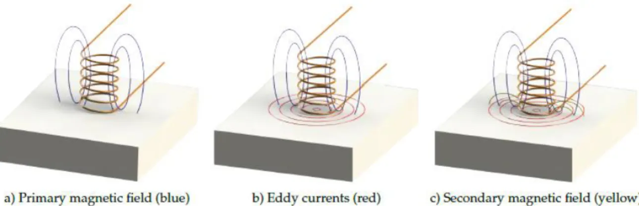
Fundamentals
An inspection coil is excited by an alternating current (AC) creating a (primary) magnetic field, according to the Biot-Savart law. When the coil approaches a conductive material (Fig. 11), the primary magnetic field (blue) induces a current (red) in the material.
According to Lenz’s Law, this induced current will create a secondary magnetic field (yellow) contrary to the first.
Fig. 11 Electromagnetic induction in eddy currents testing. Primary magnetic field (blue), generated by AC current circulating in the coil, induces an AC current (red) in the inspected part. This current creates a secondary magnetic field (yellow) that opposes the primary field.
21
Fig. 12 – Eddy Current impedance response plane [22](adapted)
This technique has low accuracy for higher depths because the density of the eddy currents decreases with depth, in a phenomenon called skin effect. In the NDT industry, the consensual limit of penetration is reached when current density is reduced to 𝑒−1≈
36.78 % of its surface value. Dept of penetration 𝛿 is given by
𝛿 = 1 √𝜋𝑓𝜎𝜇
where f [Hz]is the frequency of the alternating current in the exciting coil, σ [S/m] is the electrical conductivity and μ [H/m] is the magnetic permeability of the material. For a given material, inspection depth can be controlled by adjusting the frequency of excitation. Electrical conductivity and magnetic permeability of the material are thus the limiting factors of eddy current penetration.
Chapter 3 – Electrical Characterization
23
4.
EXPERIMENTAL PROCEDURE
4.1.
Materials
For this study AA2011 samples with 0.4% Si, 0.7% Fe, 5.0-6.0% Cu, 0.2-0.6% Bi, 0.2-0.6% Pb, 0.3% Zn, and 0.05% Ti were used. Electrical resistivity (μ) of this alloy is around
45𝑥10−9 Ω. m which corresponds to a conductivity of circa 39% IACS.
The samples were cut from a mechanically alloyed rod with 0.2 x 5 mm diameter with two different types of finishing: polished with diamond past to a mirror like-surface with sharp, as-cut edges (Type 0) and polished with sandpaper, beveled edges (Type 1) and with an orifice on the back surface to attach the thermocouple (Fig. 13).
a) b)
Fig. 13 – a) Type 0 sample mirror like-surface with sharp, as-cut edges; b) Type 1 sample polished with sandpaper and beveled edges
Chapter 4 – Experimental Procedure
24
4.2.
Nitriding Equipment
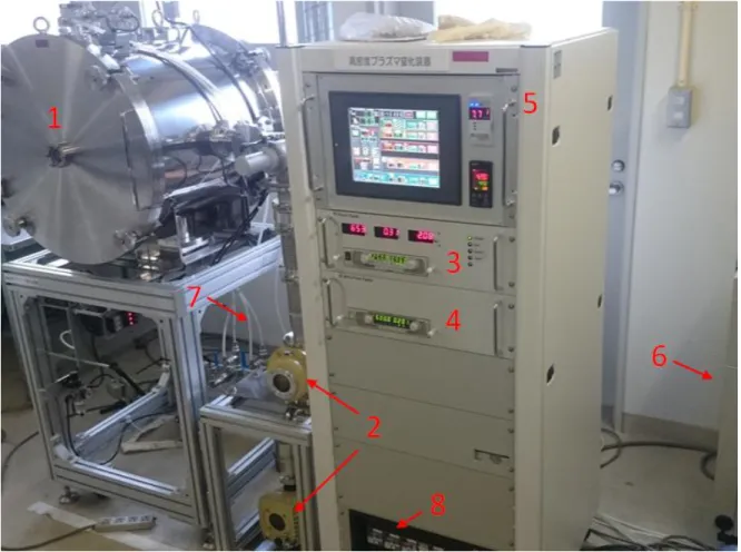
A YS Denshi nitriding machine, illustrated in Fig. 14, was used to produce samples. This is a complete plasma nitriding and ashing system specially designed for surface nitriding of steel parts, though it is also used experimentally for aluminum alloys.
It comprises a water cooled steel vacuum chamber (1), a vacuum system with a primary and a secondary pump (2), a 250 W RF dipole power supply (3), a 600 V DC bias power supply (4), a PLC controller with a control panel (5), a water cooling system(6), a gas feed system(7) and a general power supply unit (8).
Fig. 14 – Nitriding equipment: 1) vacuum chamber; 2) vacuum pumps; 3) RF power supply; 4) DC bias power supply; 5) PLC controller; 6) cooling unit; 7) gas feed lines; 8) power unit.
The control panel allows the setup of pressure (>0.1 MPa), DC bias voltage (0-600 V), RF voltage (60-250 V), 𝑁2 and 𝐻2 flow rates, each one independently from 20 to
25 The interior of the vacuum chamber, shown in Fig. 15, is composed of 1) two RF electrodes, 2) a thermocouple, 3) a heater plate and 4) a gas feed. The RF electrodes and the heater plate are supported by ceramic bushings to keep them at a different electrical potential than the chamber. The heater plate has a planar coil on the inside, to generate heat by Joule effect and it is also where DC bias is applied. The gas feed tube, not pictured here, is a 30 cm flexible steel hose.
Fig. 15 – Interior of the vacuum chamber. 1) RF electrodes, 2) thermocouple, 3) heater plate and 4) gas feed (tube not pictured).
4.3.
Parameters
Chapter 4 – Experimental Procedure
26
Tab. 1 – Sputtering and nitriding parameters of hot processed samples.
Hot samples DC (V) RF (V) P
(Pa T (℃)
Duration (s)
𝑵𝟐
(𝐦𝐥 𝐦𝐢𝐧⁄ )
𝑯𝟐
(𝐦𝐥 𝐦𝐢𝐧⁄ )
Cathode
config.
Sample
type
H1
Sputt. 500 0 70 420 1800 150 0 e) 0
Nitr. 500 250 70 420 14400 150 23
H2
Sputt. 150 0 a)
Nitr. 1800 150 23
H3
Sputt. 350 0 30 400 1800 80 0 c) 0
Nitr. 350 250 75 400 14400 80 20
H91, H92, H93
Sputt. 350 0 75 400 1800 80 0 e) 0(cover ed with
a thin steel disc) Nitr. 350 250 75 400 14400
80 20
27
Tab. 2 – Nitriding parameters cold processed samples.
Cold
samples
Heating
(℃; 𝒔) DC (V) RF
(V) P
(Pa) Duration (s)
Cathode
configuration
Sample type
H6 100;1200 400 250 70 3600 a) 0
C3; C31;
C32 86;1200 300 250 70 3600;10800;10800
a)
C41,
C42,C43, 35;150 300
250 70
14400
b) 1
C45; C46; 85;600s 300;470 18000
C47; C48,
C49 200;1260s 470 18000
C5, C51;
C52 86; 1200s
300;
400; 470 250 70 14400
b) 1(covered with a half thick disc)
T1; 86;150s 300
250 70 10800
c)
1 T11; T12;
T13; T14 35;150s 470
T2; T21 35; 150s 300 d)
B1 100;1200
470 250 70
10800
c) 1
B2 150;1200
14400 B3 180;1200
(always on)
B31 180;1200
(always on) 450
250 70 18000 c) 1
B33 180;1200
(always on) 460
A1, A2 100;1200
470 250 70
10800
e) 1
A3 150;1200 14400
Chapter 4 – Experimental Procedure
28
The following heating procedure was used for most samples: after evacuation, nitrogen was introduced until a pressure of around 300 Pa was reached; the heater was turned on for a specified amount of time, set to the desired nitriding temperature; the chamber was re-evacuated and refilled to 70 Pa; and finally the pre-sputtering was started. In some experiments the temperature measurements of the thermocouple were registered.
After having some understanding of how the plasma behaves, some modifications were made to the previous cathode configurations and new configurations were tested.
Sputtering of the cold processed samples was done at 70 Pa for 1800 s with 470 V DC (no RF), with a gas flow of 80 ml min⁄ of 𝑁2 (no 𝐻2). Sample H6 was sputtered with 400 V DC, with all other parameters equal.
A ratio of 4:1 of 𝑁2to 𝐻2 was used for nitriding in all experiments. Previous research has reported maximum hardness values of around 900 HV with this ratio [11]. Therefore, following the references as a starting point, 𝑁2 flow rate was set at 80 ml min⁄ and 𝐻2 to
20 ml min⁄ .
Research also shows that the gas content, along with other parameters, has a significant effect on the final result, since it determines which excited species are present in the plasma. This parameter requires further study to be fully understood but this is out of the scope of this thesis.
After placing the samples in the vacuum chamber pumping was carried out until the pressure reached around 0,7 Pa. Nitrogen gas was introduced to a pressure of around
300 Pa and pre-heating was performed, according to Tab. 1 and Tab. 2. After pre-heating, the chamber was evacuated again to minimize contamination. Finally, it was refilled with nitrogen at the specified pressure for each sample and pre-sputtering was initiated. About
30𝑠 before the end of the established sputtering time, hydrogen feed was started. Nitriding was initiated has soon as sputtering ended.
4.3.1. Cathode Configurations
29
a) b)
c) d)
e)
Chapter 4 – Experimental Procedure
30
4.3.2. Cover for Electrical Conductivity Tests
Some samples were partially covered in order to obtain a nitrided area, as well as a non nitrided area on the top surface. This way a direct comparison can be done between treated and untreated surfaces.
Samples H91 to H93 were covered with a thin steel disc placed in the center (Fig. 17a) while C5 to C52 were covered with a thick aluminum half disc (Fig. 17b). Samples C41 to C49 were covered, like in Fig. 17b, with Kapton tape, which later proved to be inefficient since it has around 21% of oxygen in its composition.
a) b)
Fig. 17 –Samples covered with a) a thin steel disc and b) a thick aluminum disc, to obtain an non nitrided area for reference during the electrical conductivity measurements.
4.3.3. Temperature Measurements
31
Fig. 18 – a) Location of thermocouple for sample T1 and T2; b)location of thermocouple for samples T13 and T14
4.4.
Testing
As the samples were processed, some tests were performed to determine the homogeneity of the nitride layer, its conductivity and its hardness. Initially, as soon as the specimens were removed from the vacuum chamber they were visually inspected to assess the color of the surface and its uniformity. After this the surface was inspected with the optical microscope, multimeter and SEM in order to have a qualitative overview of the result. For quantitative measurements, Vickers microindentation tests and EC tests were performed. The possibility to correlate the surface properties and the electrical conductivity data was investigated.
4.4.1. SEM
The nitrided samples were tested by Scanning Electron Microscopy with a JEOL JCM-6000 Benchtop SEM, to analyze the surface structure and morphology.
4.4.2. Electrical conductivity
Chapter 4 – Experimental Procedure
32
Fig. 19 – Eddy currents test positioning system.
33
Tab. 3 – Eddy current penetration depth of each AC current frequency
𝒇𝟏= 𝟏𝟎𝟎 𝐤𝐇𝐳 𝒇𝟐= 𝟓𝟎𝟎 𝐤𝐇𝐳 𝒇𝟑= 𝟏 𝐌𝐇𝐳
Penetration depth 𝜹 [𝐦𝐦]
0.334 0.149 0.106
The EC tests were performed in clockwise swipes with the two resolutions shown in Tab. 4. The swiping area is comprised between 𝑟 = 1 mm and 𝑟 = 9 mm, avoiding the effect of the center hole in the type 1 samples and the edge effect. For each specimen and for each frequency, two tests were performed: one to measure conductivity and one to measure lift-off. The results were plotted in 3D graphs and analyzed.
Tab. 4 – Resolution of EC tests.
Radial steps
𝑹𝒆𝒔𝝆(𝐦𝐦)
Angular increments
𝑹𝒆𝒔𝜽
Res.1 0.25 3.6°
Res.2 0.08 0.9°
4.4.3. Hardness measurements
Vickers hardness tests were performed using an Akashi MVK-H1 hardness tester. Loading time was 15 s for all samples. The applied loads varied from 10 gf to 200 gf, or 0.098 N to
Chapter 4 – Experimental Procedure
35
5.
RESULTS AND DISCUSSIONS
In this chapter the processed samples and the temperature measurements are analyzed and discussed. Results of the electrical conductivity and mechanical tests are presented and interpreted.
5.1.
Process tuning
Prior to obtaining satisfactory nitrided results, many experiments were conducted. Initially the parameters reported in the literature were used, to which some adjustments were made in what concerns DC bias, temperature and hollow cathode configurations. Other parameters like gas content, pressure and RF voltage were kept constant for all or most of the experiments. The following results are the product of iterative tuning of the nitriding process.
5.1.1. Hot processed samples
Starting with the parameters reported in [11], the result obtained was a very dark and smooth sample as seen in Fig. 20.
a) b)
Chapter 5 – Results and Discussions
36
Hardness tests of the nitrided layer were inconclusive because small loads did not produce visible indentations, suggesting an increased hardness on the surface, but, higher loads produced indentations with very distorted contours, indicating the layer was penetrated through. Vickers tests of the back of the sample revealed a decreased in hardness of the non nitrided aluminum, associated with stress relief from the heat treatment. The hardness results of 800 HV, reported in [11], were impossible to verify.
Next, the DC bias was increased from 350 V to 500 V and tested with cathode configurations a) and c). As shown in Fig. 21, the result was excessive deposition in both cases. With configuration a) the deposited layer is around 0.5 mm, it is cracked and completely detached from the substrate in some places. With configuration c) the layer is much thinner but still has adhesion problems on the edges. It is clear that 𝐴𝑙𝑁 formation is not a problem but good adhesion of the layer is.
a) b)
Fig. 21 – Samples a)H1, nitrided with cathode configuration a); and b)H2, nitrided with cathode configuration c). Both exhibit excessive nitride deposition and severe delamination.
37
a) b)
c) d)
Fig. 22 – Samples H91, H92 and H93 after processing (a, b and c) and respective cathode configuration (d).
The hot processed samples show promising results in terms of nitride layer formation but the samples showed a decrease in hardness of the substrate. This is due to stress relief, however, a heat treatment at temperatures from 250 ℃ to 400 ℃, for these processing times, will anneal every Al-Cu alloy. From an industrial view point it is important to have a nitriding process that can be applied to finished components (tempered, aged, etc.), hence the cold processed experiments were performed.
5.1.2. Cold processed samples
Chapter 5 – Results and Discussions
38
It was immediately clear with the first experiments that the process parameters would have to be tuned in order to achieve results similar to the hot processed. Fig. 23 shows the result of the first experiment that exhibited a well visible layer. There was some delamination just by handling the sample, which is a clear sign of excessive deposition. The black color on the edges indicates that these were preferential sites for deposition.
a) b)
Fig. 23 –a) Sample H6 after nitriding at 100 ℃ for 3600 s(1 h) and b) respective cathode configuration (narrow cylinder).
The cylindrical hollow cathode was replaced by a wider one in order to have more spacing between the edges of the specimen and the inner walls of the cylinder; the specimen was placed higher inside the hollow cathode, to avoid the disturbance in the plasma near the base of the tube; and the DC bias was lowered from 400 V to 300 V. These modifications should improve the gas/plasma flow around the sample and reduce the deposition rate. As can be seen in Fig. 24 the result obtained is quite interesting, since the sample is only nitrided on the bottom edges.
a) b)
Fig. 24 – a) Sample C3 after nitriding at around 100 ℃ for 3600 s(1 h); b) respective cathode configuration (wide cylinder).
39
Fig. 25 – Sample C31 after nitriding at around 100 ℃ for 10800 s(3 h).
Moving the specimen into the middle of the high density region lead to a very uniform color of the nitrided layer. This can be seen in Fig. 26, were the sample has a dark grey color, on the top surface and on the edges, and no delamination. This result is similar to those of the hot processed experiments, which suggests that the process is feasible at lower temperatures.
Fig. 26 -Sample C32 after nitriding for 10800 s(3 h), at 300 V, starting at 86 ℃.
Next, the effect of the beveled edges was tested. Using cathode configuration a) the result was a light grey colored surface with slightly darker edges, after 5 h of nitriding (Fig. 27). This suggests that the less sharp edges may be unfavorable in the formation of the nitrided layer.
a) b)
Fig. 27 - Sample C49 after nitriding for 18000 s (5 h) at 470 V, starting at 196 ℃, without heating during the process; respective cathode configuration.
Chapter 5 – Results and Discussions
40
but it is not uniform. The quality of the layer seems to be highly dependent on the geometry of the workpiece.
d)
Fig. 28 – a) C51 with 470 V DC bias; b) C52 with 400 V DC bias; c) C5 with 300 V DC bias. All nitrided for 14400 s(4 h), starting at 86 ℃, without heating during the process.
Changing to cathode configuration c) lead to more satisfactory results, as can be seen in Fig. 29. After 4 h of nitriding, starting the process at 150 ℃, the surface was still darker on the edge and it had some nitride clusters. Raising the process temperature to a constant
180 ℃, lead to a uniform, dark grey, though there were even more nitride clusters on the surface that increased its roughness significantly. It should be noted that the processing temperature was the only parameter that changed. The differences seen in Fig. 29 were either caused by the difference in temperature or by other unmeasured factor (e.g. electrical contact between cathode parts, position of sample, etc.).
Fig. 29 – Samples B2 and B3 after nitriding for 14400 s (4 h), at 470 V, starting at 150 ℃ and 180 ℃, respectively.
41 successfully avoided but the color of the surface, especially on the edges, is much lighter, indicating a thinner coating. Longer processing times may produce better results.
a) b)
Fig. 30 – a) sample B31 (450 V DC bias); b) sample B34 (460 V DC bias); both nitrided for 18000 s (5 h) at 180 ℃.
All beveled samples exhibit some nitride clusters on the top surface when nitrided with cathode configuration c), therefore, a small change was made. The hollow cathode was moved to the center of the heater plate and placed on top of a steel cylinder. The objective was to find a location where the plasma field is more uniform. This is the configuration seen in Fig. 16e).
The result of this experiment is shown in Fig. 31b). There seems to be a uniform distribution of the layer but the color is very light.
a) b) d)
Fig. 31 – Samples a)A1, placed at the entrance of the hollow cathode; and b)A2, placed 3 4⁄ length inside the hollow cathode. Both pre-heated to 100 ℃ and nitrided with 470 V DC for 10800 s (3 h). d) Cathode configuration used in these
experiments.
Chapter 5 – Results and Discussions
42
To improve upon these results, the nitride layer should be made thicker while maintaining the good homogeneity seen in Fig. 31b). For this purpose the temperature was increased to 150 ℃, and then 180 ℃, as well as the processing time, from 3 h to 4 h. Fig. 32 shows the results obtained.
a) b)
Fig. 32 – Samples a)A3, pre-heated to 150℃; and b)A4, constant temperature of 180℃. Both nitrided with 470 V DC, for 14400s (4h) and with cathode configuration e)
Both results present a dark color, though with some reflectiveness, and a good distribution of the layer. At 180 ℃ the edges seem to have been more nitrided than the center. Incresing the processing time further, maintaining this temperature, might have provided better results. The 𝐴𝑙𝑁 clusters seen previously are not present here. Configuration e) seems to be the most adequate for these experiments.
5.2.
Effects of cathode configuration and DC bias on temperature
43
Fig. 33 – Temperature measurements of samples C32, nitride with cathode config a), and C32, nitrided with cathode config. b). Thermocouple on the heater plate.
Since during the pre-sputtering phase both temperatures decreased and, during the nitriding phase C49 maintained a relatively high temperature and C32 increased its temperature, it is safe to assume that a considerable amount of heat is supplied to the cathode during the second phase. The source of this heat must be the high density plasma created inside the hollow cathode due to the strong magnetic field.
It is interesting to see that sample C32, at a much lower temperature and with lower DC bias, seems to be darker in color and more homogeneous than C49, indicating that workpiece geometry (sharp vs beveled edges) and surface roughness may be relevant factors for layer formation.
The temperatures measured with configuration c), namely of samples B1, B2 and B3, are plotted in Fig. 34. Sample B1 increased temperature during the entire process, from 100℃ to 160℃, with a tendency to stabilize at the end. B2 started at 150℃, decreased to 140℃ during pre-sputtering and increased during nitriding to a stable 165℃. B3 was made at constant temperature, with only minor oscillations.
70.0 90.0 110.0 130.0 150.0 170.0 190.0 210.0
0 2000 4000 6000 8000 10000 12000 14000 16000 18000 20000 T(°C)
t(s)
Config. a) and b)
C49(470V)
Chapter 5 – Results and Discussions
44
Fig. 34 – Temperature measurements of samples B1 (pre-heated to 100 ℃), B2 (pre-heated to 150 ℃) and B3 (heated to 180 ℃ throughout). All nitride with cathode config c) and 470 V DC bias. Thermocouple on the heater plate.
Fig. 35 shows the temperature measurements done on samples A2, A3 and A4 using configuration e). Every parameter, except for cathode configuration, is the same as in the B samples (A1 analogous to B1, A2 analogous to B2, etc.) so configurations c) and e) can be compared directly.
Fig. 35 - Temperature measurements of samples A2 (pre-heated to 100 ℃), A3 (pre-heated to 150 ℃) and A4 (heated to 180 ℃ throughout). All nitride with cathode config e) and 470 V DC bias. Thermocouple on the heater plate.
As can be seen the temperatures follow the same tendencies though, for A2 and A3, the maximum temperatures registered are lower than those of B1 and B2. This may be because configuration e) takes longer to reach thermal equilibrium in all the cathode pieces, since the hollow cathode is further away from the heater plate.
70.0 90.0 110.0 130.0 150.0 170.0 190.0 210.0
0 2000 4000 6000 8000 10000 12000 14000 16000 18000 20000 T(°C) t(s)
Config. c)
B1(470V) B2(470V) B3(470V;180ºC) 70.0 90.0 110.0 130.0 150.0 170.0 190.0 210.045 Temperatures measured with cathode configuration c) and d), are plotted together in Fig. 36. As can be seen, starting the process at a temperature of around 35 ℃, both configurations achieve similar maximum temperatures bellow 170 ℃. Configuration c) has an increasing heating rate until around 1 h 30 min of starting the pre-sputtering (5400 s), after which it decreases to a steady value until the end of the process. Configuration d) has a very high heating rate on the first seconds of pre-sputtering but, after around 1000 s of processing, the heating rate decreases to a steady value similar to that of c).Towards the end, the temperature of configuration c) surpasses that of d), hinting that the former might achieve higher temperatures for longer processing times.
Fig. 36 – Temperatures measured on the heater plate, using c) and d) cathode configurations with 300 V DC bias(samples T1 and T21, respectively)
These experiments were performed with pre-heating only, hence, it should be noted that a considerable amount of heat is supplied by the plasma since the temperatures achieved in both are just below those seen in Fig. 34.
Temperature on the surface of the sample
The temperatures measured at the surface of the sample, for cathode configurations c) and d), are plotted in Fig. 37.
0.0 20.0 40.0 60.0 80.0 100.0 120.0 140.0 160.0 180.0
0 1000 2000 3000 4000 5000 6000 7000 8000 9000 10000 11000 12000 13000 T(°C)
t(s)
Config. c) and d)
cathode config. c)
Chapter 5 – Results and Discussions
46
Fig. 37 – Temperatures measured at the surface of the sample with longitudinal (L) and transverse (T) hollow cathode configurations at 300 V DC bias.
During most of the pre-sputtering, both the longitudinal and the transverse configurations show the same temperatures. As soon as the hydrogen is introduced (1770 𝑠), the temperature c) starts to decrease, with some oscilations, while the temperature of d) continues to increase. When the RF is turned on (1800 𝑠), the temperature of c) suffers a considerable decrease, after which the rate of increase is low; and the longitudinal sample continues to increase slowly until it stabilizes at 6000 𝑠, just below 400 ℃.
During pre-sputtering, because only the DC bias is on, the plasma has the same behavior in both cathode configurations. When the RF is turned on, magnetic fields and eddy currents are generated inside the chamber and in the hollow cathode. Each cathode configuration interacts differently with the generated magnetic field, hence the difference in measured temperatures.
The transverse configuration presents the lowest average temperatures on the surface of the sample in spite of the higher temperature during the pre-sputtering phase. However, since this measurement was taken with the thermocouple wire in the middle of the high density plasma region, it may be inaccurate. Additional experiments are necessary.
Analyzing Fig. 38, it can be seen that this temperature peak at the surface of the sample is not detected when measuring on the heater plate, which may indicate that it is a localized temperature spike that does not affect the substrate. The temperatures plotted are for processes with different DC bias voltages, therefore only the gradients can be compared, not the temperature values.
0.0 50.0 100.0 150.0 200.0 250.0 300.0 350.0 400.0
0 1000 2000 3000 4000 5000 6000 7000 8000 9000 10000 11000 12000 13000 T(°C)
t(s)
Config. c) and d), surface of sample
cathode config. c)
![Fig. 1 – Aluminum rich section of the Al-Cu phase diagram. [1]](https://thumb-eu.123doks.com/thumbv2/123dok_br/16560132.737535/23.918.141.782.332.826/fig-aluminum-rich-section-al-cu-phase-diagram.webp)

![Fig. 6 – Schematic example of radio frequency plasma nitriding equipment [5].](https://thumb-eu.123doks.com/thumbv2/123dok_br/16560132.737535/31.918.281.634.638.972/fig-schematic-example-radio-frequency-plasma-nitriding-equipment.webp)
![Fig. 7 – Nitride layer thickness has function of nitriding time for Al 1100 [9].](https://thumb-eu.123doks.com/thumbv2/123dok_br/16560132.737535/33.918.238.684.118.405/fig-nitride-layer-thickness-function-nitriding-time-al.webp)
![Fig. 10 – AlN formation on the surface of pure aluminum in nitrogen-hydrogen atmosphere [7]](https://thumb-eu.123doks.com/thumbv2/123dok_br/16560132.737535/35.918.135.788.427.715/fig-aln-formation-surface-aluminum-nitrogen-hydrogen-atmosphere.webp)