Eduardo Costa Girão
Propriedades eletrônicas e de transporte de
nanoestruturas de carbono
–
Electronic and transport properties of carbon
nanostructures
Fortaleza - CE
Propriedades eletrônicas e de transporte de
nanoestruturas de carbono / Electronic and transport
properties of carbon nanostructures
Tese apresentada ao Curso de Pós-Graduação em Física da Universidade Federal do Ceará como parte dos requisitos para a obtenção do título de Doutor em Física.
Prof. Antônio Gomes Souza Filho / Prof. Vincent Meunier
DOUTORADO EMFÍSICA
DEPARTAMENTO DE FÍSICA
CENTRO DE CIÊNCIAS
UNIVERSIDADEFEDERAL DO CEARÁ
Fortaleza - CE
Tese de Doutorado sob o título Propriedades eletrônicas e de transporte de nanoestru-turas de carbono / Electronic and transport properties of carbon nanostructures, defendida por Eduardo Costa Girãoe aprovada no dia 20 de Dezembro de 2011 em Fortaleza, Ceará, pela banca examinadora:
Prof. Antônio Gomes Souza Filho
Departamento de Física - Universidade Federal do Ceará Advisor
Prof. Vincent Meunier
Department of Physics, Applied Physics, and Astronomy -Rensselaer Polytechnic Institute
Advisor
Prof. Antônio José Roque da Silva Laboratório Nacional de Luz Síncrotron and Instituto de Física - Universidade de São Paulo
Prof. Douglas Soares Galvão
Instituto de Física ‘Gleb Wataghin’ - Universidade Estadual de Campinas
Prof. François M. Peeters
Department of Physics - University of Antwerp
Prof. Humberto Terrones
Department of Physics - The Pennsylvania State University and Departamento de Física - Universidade Federal do
Acknowledgements
Well, I have to thank a lot of people.
First of all, I thank God for everything. Each person knows his/her life experiences better than anyone else and, in my case, I know the importance He has in my life. I thank Him for showing me where to go and for giving me all the tools I needed to construct everything I have.
I thank my wife, Adriana, for being by my side for the last 11 years. I can not imagine my life without her. I thank her for the good moments, because they made us happy, and also for the bad ones, because they made us stronger. Along these years together, we made right and wrong choices, but the best choice I made was you. Thank you for letting me be your choice.
I thank my family for being my first support, my first school. Despite my defects, I am very happy with who I am and a great part of it was constructed with what I learned from my parents. Thanks for being strong when distant, thanks for being lovely when close.
I thank Professor Antônio Gomes Souza Filho for being my advisor since I was an under-graduate student. It has been hard to work with completely different tools, but you have always tried to direct me to the right path. I thank you for being sincere in all the stages of my academic trajectory. In special, I thank you for not letting me to take the wrong choice. Your calm was fundamental to show me the best decision to make and it has conducted me to a position from where I can see good things ahead.
I thank Professor Josué Mendes Filho for the motivation. I had some tough moments during my the academic path, but the few words I heard from him during these times were enough to make me confident that I could get over the problems and make a good job at the end.
I thank Professor Solange Binotto Fagan for introducing me to the field of theoretical cal-culations. Today I’m very happy with the area I chose to work and you have great influence on this decision. Thanks for your advising when I was a undergraduate, during the master’s and in part of my PhD.
I also thanks the other guys from Oak Ridge, Viviane, Álvaro, Miguel, Paschoale, Bobby, and Deb Holder. Staying far from home in a place you do not know is usually hard, specially in the beginning, but you guys made it all easier for me and make me fell a little more like home.
I also thank Professor Humberto Terrones who I meet in Oak Ridge. It has been very good changing ideas with you. I hope we have more opportunities for coffee time. I thank you for you support in Oak Ridge and here in Fortaleza.
I have had a great time in Troy. Work made me happy there, but I also made good friends. My days always got better after a ride in the “Red Hawk Shuttle”. Karen, James, Sean and all the other drivers made my everyday easier after the ride and nicer after the chat. I want you to know that your work and friendship were very important to me. Thanks a lot.
While being in US, I could still fell a little like in Brazil. This is because Adriana and I had our friends “Don” Fernando and Sônia and their kids Mariel, Nicolas and Gabriela. We have had very good moments in Troy and I really want this friendship to last forever. Fernando, I will never forget that crazy journey to New York city, that was a lot of fun. Thank you guys for the help and friendship.
Leo is another good friend I made in Troy. Together with Adriana, we had a lot of fun hanging out. It was very nice working with you everyday and I wish you all the best in your PhD. Thanks for the friendship.
Even though I have already cited Dr. Eduardo Cruz-Silva, I need to dedicate some more lines to him. Lalo helped me like a brother. His help with the arrangements for my arrival in Oak Ridge were enough to make me grateful. But once I got to Oak Ridge, I had the opportunity to know him better. More than I expect, Lalo revealed to be a great friend. But there is more. Lalo is great researcher and I am also happy for having the chance of changing ideas and making science with him. Lalo and his lovely wife Marcia are friends that will always be in my heart. Thanks you guys for everything.
I also thank my friends from the Physics Department in UFC. Well, I know these guys for almost 10 years and I thank God for giving me such good friends. Time goes by and we are naturally getting far from each other, but the friendship is the same and I thank you guys for all the support and the good moments. I really wish all the best for you.
Abraão stayed away from physics for some time, but even in that time, he was a close friend and his support was very important to me. We are now geographically far from each other, but there is no distance for friendship. I wish success for your guys in the new challenges you are about to face.
I have another special thank to my friends Antônio Márcio and Lavor for their attention when hosting me and Adriana in Recife.
I also thank all my other friends not related to the University. Each of you guys have, somehow, a special contribution for my achievements.
I thank Oak Ridge National Laboratory for all the support during my stay in Tennessee.
I thank Rensselaer Polytechnic Institute all the support and for providing me the best work environment I have ever had to develop my work.
I thank Universidade Federal do Ceará for all the support during my whole academic life.
I thank Brazilian agency CNPq for the precious financial support which made it possible for me to develop my academic work when I was as undergraduate student, as well as during my master’s and PhD.
I thank Brazilian agency CAPES for the financial support during my stay in USA through the sandwich program fellowship.
I thank my colleagues from Universidade Federal do Piauí, specially Professors Bartolomeu Cruz Viana Neto and Cleânio da Luz Lima, for all the support during my initiation in the institution.
Resumo
À medida que o limite de miniaturização da eletrônica baseada no silício aproxima-se do seu limite, alternativas em estado sólido devem ser investigadas na busca da diminuição da escala de tamanho de dispositivos operacionais, ao mesmo tempo em que se deve considerar problemas de crescente interessse como dissipação de calor e ruído associado com a baixa di-mensionalidade. Nesta busca, já está claro que nanosistemas semicondutores de carbono são candidatos de primeiro pelotão para comporem os blocos básicos para dispositivos em escala atômica e molecular. Grafeno e nanotubos de carbono são os sistemas mais estudados desta classe de estruturas que se estende por uma vasta coleção de sistemas. Estas nanoestruturas de carbono apresentam uma riqueza de propriedades físicas e químicas que se reflete no enorme número de artigos científicos tendo esses sistemas como foco [1]. Apesar de a ciência das na-noestruturas de carbono ainda ter um longo caminho pela frente antes de alcançar as prateleiras das lojas depois de ter sido transformada em tecnologia, a comunidade científica tem caminhado rapidamente no sentido de entender e controlar tais sistemas de modo a diminuir esta distância.
Nesta tese nós realizamos um estudo teórico das propriedades eletrônicas e de transporte de um número de nanoestruturas de carbono, tais como nanosistemas toroidais e nanofitas de car-bono de arranjo complexo. Nossos cálculos de estrutura eletrônica são baseados em um modelo tight-binding que inclui um Hamiltoniano de Hubbard para descrever a influência do spin sobre os estados eletrônicos. As propriedades de transporte eletrônico foram calculadas utilizando o formalismo de Landauer e o método de funções de Green para determinar a transmitância quântica em sistemas em nanoescala. Parte destes cálculos foram realizados com pacotes com-putacionais desenvolvidos especialmente para esta tese. Em particular, nós desenvolvemos uma extensão de um algorítmo eficiente para o cálculo de função de Green em uma infraestrutura computacional em paralelo.
trutura atômica destaswigglespode ser descrita por um conjunto reduzido de fatores já que elas podem ser construídas utilizando-se fitas de carbono de borda reta como blocos básicos. Nós mostramos que essaswigglesde carbono apresentam um conjunto de propriedades eletrônicas e magnéticas ainda mais amplo quando comparadas com os seus constituintes básicos (fitas de carbono de borda reta). Isso é especialmente devido à formação de domínios nas bordas, resul-tantes da sucessiva repetição de setores de fitas retas paralelas e obliquas ao longo da direção periódica dawiggle. Nós demonstramos que aswigglesde carbono apresentam múltiplos es-tados magnéticos que podem ser explorados para se manipular as propriedades físicas desses sistemas. Estes diferentes estados magnéticos resultam em propriedades eletrônicas e de trans-porte distintas, de modo que a corrente eletrônica pode ser controlada pela escolha de valores específicos da energia do elétron incidente no sistema, assim do spin eletrônico e do estado magnético da wiggle. Essas propriedades tornam as nanowiggles potenciais candidatas para novas aplicações em nanodispositivos.
Abstract
As the miniaturization limit of the physical size of Si-based electronics is projected to be reached in a near future, solid-state alternatives must be investigated in the pursuit of further scaling down the effective operational device structures, while considering growingly important problems such as heat dissipation and noise associated with reduced dimensionality. In this quest, it is clear that semiconducting carbon nanosystems are solid front-runner candidates to compose the building blocks for devices at molecular and atomic scales. Graphene and carbon nanotubes are the most studied members of this class of structures which extends over a broad collection of systems. These carbon nanostructures present a wealth of promising physical and chemical properties which is reflected in the number of scientific works having these systems as focus [1]. Even though the science of carbon nanostructures has a long path ahead before reaching the shelves of stores after being transformed into technology, the scientific community has been walking fast towards the understanding and the control of such systems in order to shorten this gap.
In this thesis we theoretically studied the electronic structure and transport properties of a number of carbon nanostructures, such as toroidal carbon nanosystems and complex assembled graphitic nanoribbons. Our electronic structure calculations are based on a tight-binding model including a Hubbard Hamiltonian to describe the influence of spin on the electronic states. The electronic transport properties were computed using the Landauer formalism and a Green’s function approach to determine the quantum transmission in nanoscaled systems. Part of these calculations were performed with computational packages developed specifically for this the-sis. In particular, we developed an extension of an efficient algorithm to calculate the Green’s function on a parallel computational infrastructure.
Carbon nanotori display specific electronic structure compared to carbon nanotubes, since this geometry imposes a supplemental degree of spatial confinement. As a consequence, addi-tional conditions on the structure geometry have to be obeyed for a given torus to be metallic. Here we analyzed carbon nanotori from two different perspectives: two-terminal systems with a variable angle between the terminals and multi-terminal structures. These rings are potential systems for nanoelectronic application as their particular geometry allows the current to flow through the system along different electronic paths. This results in interesting transport proper-ties dictated by electron interference effects which vary with the angle between the electrodes and the atomic details of the nanotorus-electrode junction. We showed that the presence of multi-terminals adds new features to the electronic transport on these tori as the number of pos-sibilities for the electronic flow increases quickly with the number of electrodes. It turns out that the conductance is characterized by a set of resonant peaks which are related to specific electronic paths. These results are rationalized into a set of rules to determine the path for the electrical current as a function of the impinging electron energy.
and magnetic properties in comparison to those of their constituents (graphene nanoribbons). This is mainly due to the formation of edge domains resulting from the successive repetition of parallel and oblique graphene nanoribbon sectors along the wiggle’s periodic direction. We demonstrate that carbon wiggles present multiple magnetic states which can be exploited to tune the physical properties of these systems. These different magnetic states lead to dissimilar electronic structure and transport properties for the wiggles so that the electronic current on these systems can be tuned by selecting specific values for the impinging electron energy as well as its spin and the wiggle’s magnetic state. These properties make carbon nanowiggles potential candidates as new nanodevices.
Contents
List of Figures
List of Tables
Prologue p. 28
I Generalities
30
1 Introduction to nano carbon p. 31
1.1 Atomic electronic structure . . . p. 31
1.2 Hybridization . . . p. 35
1.2.1 sphybridization . . . p. 35 1.2.2 sp2hybridization . . . p. 35 1.2.3 sp3hybridization . . . p. 36 1.2.4 spδ hybridization . . . p. 37 1.2.5 What is so special about carbon? . . . p. 40
1.3 Carbon nanotubes . . . p. 42
1.3.1 Nanotube’s structure . . . p. 42
1.3.2 Electronic structure . . . p. 44
1.4 Graphene and graphitic ribbons . . . p. 48
1.4.1 Graphene nanoribbons . . . p. 48
1.4.2 Graphene nanoribbons synthesis . . . p. 52
1.7 Economic and societal considerations . . . p. 57
1.8 This thesis . . . p. 58
2 Methods to calculate the electronic band structure of solids p. 59
2.1 Hamiltonian . . . p. 59
2.2 Electronic problem . . . p. 60
2.2.1 Hartree method . . . p. 60
2.2.2 Hartree-Fock (HF) method . . . p. 61
2.2.3 Density Functional Theory . . . p. 62
2.3 Localized Basis . . . p. 65
2.4 Hamiltonian elements . . . p. 67
2.5 Bloch functions . . . p. 69
2.6 The Slater-Koster approach . . . p. 71
2.7 Graphene . . . p. 73
2.8 The TBFORproject . . . p. 75
2.8.1 Hamiltonian . . . p. 75
2.8.2 Eigenfunctions . . . p. 76
2.8.3 Eigenvalues . . . p. 77
2.8.4 Hubbard model . . . p. 78
2.8.5 Self-consistency . . . p. 81
2.8.6 Mixing schemes . . . p. 81
2.9 Overview . . . p. 83
3 Electronic transport at the nanoscale p. 84
3.1 System description . . . p. 84
3.3 Transmission and reflection . . . p. 86
3.4 Experimental evidences of conductance quantization . . . p. 90
3.5 The Green’s function formalism . . . p. 92
3.6 Green’s function and density of electronic states . . . p. 95
3.7 Green’s function and Landauer formalism . . . p. 96
3.8 Electrodes: infiniteversusfinite matrices . . . p. 99 3.9 Electrode’s surface GF: iterative method . . . p. 100
3.10 Electrode’s surface GF: transfer matrices . . . p. 103
3.11 Non-orthogonal basis . . . p. 105
3.12 The next step . . . p. 105
4 Conductor Green’s function p. 106
4.1 Introduction . . . p. 106
4.2 Dyson’s equation . . . p. 107
4.3 Setup . . . p. 108
4.4 Knitting Algorithm . . . p. 110
4.5 Sewing Algorithm . . . p. 111
4.6 Multiple Knitting and Domains Approach - Patchwork Algorithm . . . p. 115
4.7 Sewing algorithm in the domain approach . . . p. 118
4.8 The TRANSFORproject . . . p. 118
4.9 Overview . . . p. 121
II Nanotori
122
5 Toroidal carbon nanostructures - two terminal systems p. 123
5.1 Carbon nanorings . . . p. 123
5.4 Numerical Results . . . p. 132
5.5 Quantum interference model . . . p. 139
5.6 Overview . . . p. 142
6 Toroidal carbon nanostructures - multi terminal systems p. 144
6.1 Tubular and flat nanorings . . . p. 144
6.2 Numerical results - TNs . . . p. 146
6.3 Numerical results - FNs . . . p. 148
6.4 Overview . . . p. 151
IIINanowiggles
154
7 Graphene carbon nanowiggles - geometric considerations p. 155
7.1 Introduction . . . p. 155
7.2 GNW’s structure . . . p. 156
7.3 Lattice parameter . . . p. 157
7.3.1 General approach . . . p. 157
7.3.2 Thel length . . . p. 159 7.3.3 Thew,handblengths . . . p. 160 7.3.4 Lattice parameter relations . . . p. 161
7.4 Number of atoms . . . p. 161
7.4.1 Healed GNW’s widthW and wedge’s heightH . . . p. 162
7.4.2 Wedge’s basisB andB′ . . . p. 162
7.4.3 Formulas forN . . . p. 163
7.4.4 Corrections on the AA-GNW case . . . p. 163
7.6 Summary of results . . . p. 166
8 Graphene carbon nanowiggles - Electronic properties p. 169
8.1 Introduction . . . p. 169
8.2 Theoretical Methods . . . p. 170
8.3 Multiple magnetic states . . . p. 171
8.4 AA-GNWs . . . p. 173
8.5 AZ-GNWs . . . p. 173
8.6 ZA-GNWs . . . p. 180
8.7 ZZ-GNWs . . . p. 182
8.8 Overview . . . p. 187
9 Graphene carbon nanowiggles - electronic transport properties p. 188
9.1 Methods . . . p. 188
9.2 AZ-GNWs . . . p. 189
9.3 ZA-GNWs . . . p. 192
9.4 ZZ-GNWs . . . p. 197
9.5 From the one cell system to the periodic system . . . p. 200
9.6 Summary . . . p. 202
Conclusions p. 203
Perspectives . . . p. 205
Appendix A -- Input examples for TBFOR p. 207
Appendix B -- Generating GNWs coordinates: utility program p. 210
Appendix C -- Publications p. 219
List of Figures
1.1 Radial functions for the first threes(a) and p(b) orbitals. . . p. 33 1.2 Spherical harmonics for thes(a) and p(b) orbitals. . . p. 34 1.3 (a)sp,(b)sp2and (c)sp3hybridization schemes and corresponding examples. p. 36 1.4 Bonds for a carbon atom in a (12,0) nanotube and the corresponding spδ
hybrid orbitals. . . p. 38
1.5 Coefficients for thesorbital in thesp2andsp3hybridization schemes and for thespδ case for a(n,0)nanotube (a) as a function ofnand for a CHCl3like
molecule (b) as a function ofθ. . . p. 39
1.6 Bonds for a carbon atom in a C60 fullerene (a) and thespδ hybridization for
aCHCl3-like molecule (b). . . p. 39
1.7 Energies for the 2sand 2porbitals as a function of the atomic number for the
atoms in the second row of the periodic table [2]. . . p. 41
1.8 (a) Graphene honeycomb lattice and the vectors defining a nanotube unit cell;
(b) A graphene sheet piece being rolled up to form a nanotube. . . p. 43
1.9 Examples of zigzag, armchair and chiral nanotubes. . . p. 44
1.10 Illustration of the quantum confinement along the circumferential direction in a carbon nanotube and the corresponding cutting lines over graphene’s
Brillouin zone. . . p. 46
1.11 Cutting lines over graphene’s Brillouin zone for the nanotubes(12,0),(6,6),
(8,2)and(10,0). . . p. 47
1.12 Electronic band structure for the (12,0) (a), (6,6)(b), (8,2) (c) and(10,0)
(d) nanotubes obtained with the zone-folding-tight-binding method. Here we
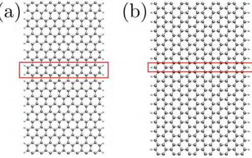
level is atE=0. . . p. 48 1.14 Basic structures for A-GNRs (a) and Z-GNRs (b). The red boxes indicate the
GNRs unit cells. . . p. 49
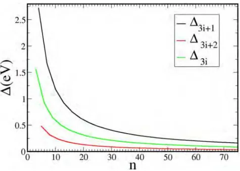
1.15 Electronic band gap∆for an A-GNR as a function of the numbernofC−C
lines. The three families correspond ton=3i+jwith j=0,1,2. . . p. 50
1.16 Paramagnetic (PM), anti-ferromagnetic (AFM) and ferromagnetic (FM) states in a Z-GNR and their corresponding band structures (green line is the Fermi
energy, and black and red lines stand for spin up and down levels). . . p. 51
1.17 Energy difference between any pair of different states in a Z-GNR with n=
3, ...,40. . . p. 52
1.18 Different proposed ELD geometries in graphene [3]. . . p. 52
1.19 (a) Illustration of the bottom-up approach developed by Cai et al. to obtain graphene nanoribbons with clean armchair edges. (b-c) Different molecular precursors for the procedure illustrated in (a) and their corresponding final
products. Adapted from [4]. . . p. 53
1.20 R5,7,H5,6,7andO5,6,7planar haeckelites structures [5]. . . p. 55
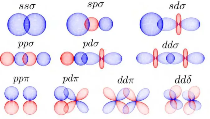
2.1 Spherical harmonics in theYl,±|m|form. . . p. 67 2.2 Different two-center integrals schemes for the Hamiltonian elements on a
localized basis. . . p. 69
2.3 Graphene and lattice vectors definition. . . p. 73
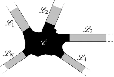
3.1 Basic system for electronic transport calculations. A central scattering region
C coupled to the semi-infinite terminalsL1,L2,L3,L4, ...,LN. . . p. 84
3.2 Semi-infinite terminal and the corresponding Hamiltonian sectors. . . p. 85
3.3 Dependence of the quantum conductance on the gate voltage for a quantum
4.1 Illustration of the knitting procedure for a 9-site system with first-neighbor interactions only. We start with a set of non-interacting sites. By adding site number 2, we consider its interaction with the previous site number 1. When adding 3, we should account for its interaction with previous sites 1 and 2 (interaction 2-3 is null in this case). As the process is conducted, we finish by adding site 9 accounting for its interactions with all the previous atoms (non-null only for sites 6 and 8 in this case). After adding all the sites we
have the final GF. . . p. 108
4.2 Illustration of the patchwork algorithm for a finite 2D system with only first-neighbor interactions and initially divided into four domains. The first patch-work step consists in adding all the DIAs (green atoms) from each domain, while not considering the DSAs (red atoms). Once we add all the DIAs we redefine the domains by merging them two-by-two. Some previously DSAs become DIAs which will be added in this second patchwork step (DIAs added in a previous patchwork step are painted in blue). We carry out this process until we have a single domain which, after having all its DIAs added,
pro-vides the final GF. . . p. 116
4.3 Quantum conductance (using knitting algorithm) and DOS (using sewing al-gorithm) for the nanotubes(8,0),(7,7)and(12,0). We used a first-neighbor
TB model withγ =3.0 eV ands=0. The Fermi energy is set to 0.0. . . p. 119 4.4 Quantum conductance as a function of energy for (6,6), (12,0) and(10,0)
carbon nanotube based tori attached to two semi-infinite terminals making an angle of 180◦calculated by the TRANSPLAYER (black lines) and
TRANS-FOR (red lines) packages. We used a first-neighbor TB model withγ =3.0
eV ands=0. The Fermi energy is set to 0.0. . . p. 120 4.5 Time for 10 knitting steps versus number of processors (red lines) for a
(10,10) nanotube with 1250 cells as CSR (average over 10 calculations) in
direct (upper panel) and logaritmic (lower panel) scales. Black lines represent
the corresponding curves for perfect scaling. . . p. 121
5.1 Systematic procedure to generate a torus from a nanotube. . . p. 125
5.2 Schematic representation of the procedure adopted for the systematic
struc-ture construction. . . p. 126
Brillouin Zone. The spacing for the two families of lines are directly related
to the curvatures of the nanotube (1/r) and the nanotorus (1/R). . . p. 128
5.5 (a)-(c): Cutting lines near aK point for(8,2)nanoring with 119 (a), 120 (b)
and 121 (c) nanotube units cells, respectively; (d)-(e): Electronic density of
states for the (8,2) and (6,6) nanotori made up of 120 nanotube cells [7]. . . . p. 129
5.6 Conductance versus energy and α for the α1803◦ ◦ and α3 ◦
178.5◦ series for the
(12,0)r−(12,0)t (a-b) and(10,0)r−(10,0)t systems (c-d), respectively [7]. p. 134
5.7 DOS, conductance, and LDOS for the α =180◦ (a) and 178.5◦ (b) in the
(10,0)r−(10,0)t systems [7]. . . p. 135
5.8 Conductance versusenergy andα for theα1809◦ ◦ (a), α9 ◦
177◦ (b), α9 ◦
174◦ (c) and
α1789◦ .5◦ (d) series for the(6,6)r−(6,6)t system. The white lines are
isocoun-tour lines for the model described in Section 5.5 [7]. . . p. 136
5.9 DOS, conductance, and LDOS for the α =180◦ (a) and 178.5◦ (b) in the
(6,6)r−(6,6)t system [7]. . . p. 137
5.10 Conductance versusenergy andα for theα1809◦ ◦ (a), α1779◦ ◦ (b), α1749◦ ◦ (c) and α1789◦ .5◦ (d) series for the(8,2)r−(8,2)t systems. The white lines are
isocon-tour lines for the model described in Section 5.5 [7]. . . p. 138
5.11 (a) Concept of the wave interference model. (b) Scaterring processes
under-going in the junctions. . . p. 139
5.12 Conductance versus energy and α for the α1803◦ ◦ in the (12,0)r−(12,0)t
(a) and(10,0)r−(10,0)t systems according to the model described in
Sec-tion 5.5 [7]. . . p. 142
6.1 Carbon nanotoroid structures studied in this chapter: (a) TNs and (b) FNs [8]. p. 145
6.2 Conductance for the different paths on the(6,6)nand(12,0)n,n=2,3,4,5,6
structures [8]. . . p. 147
6.3 Conductance for the different paths on the (6,6)n and (12,0)n, n= 8,10,
structures [8]. . . p. 148
6.5 Conductance for the different paths on the[6,6]n(n=2,3,4,5,8) and[12,0]n
(n=2,3,4,5,6) [8]. . . p. 150
6.6 Conductance for the different paths on the [6,6]n (n= 6,10) and [12,0]n,
(n=8,10), structures [8]. . . p. 152
6.7 Conductance for the different paths on the[6,6]12 and[12,0]12 structures [8]. p. 153
7.1 (a) Geometry and nomenclature of a GNW made up of successive oblique and parallel cuts in armchair (A) or zigzag (Z) patches. (b-e) Examples of an
AA (b), AZ (c), ZA (d) and ZZ (e) GNW. . . p. 156
7.2 Schematic construction of the four achiral GNWs: initial GNR and the
trape-zoidal wedges needed to transform it into a GNW. . . p. 157
7.3 Definition of theWp andWoparameters as the lines ofC−C lines or zigzag
strips along the width of each sector. Here the example of an AZ-GNW with
Wp=7 (red lines) andWo=5 (green lines). . . p. 158
7.4 Definition of the Lp as the number ofaCC lengths (AA- and AZ-GNWs) or
zigzag tips (ZA- and ZZ-GNWs) along the smallest basis of the trapezoid formed by the GNW’s edge atoms. Here the example of an AZ-GNW with
Lp=5 (left) and a ZZ-GNW withLp=3 (right). . . p. 158
7.5 Auxiliary lengths to determine the lattice parameter of a general GNW unit
cell. . . p. 158
7.6 Auxiliary lengthl for ZA-GNWs (a) and increment f for ZZ-GNWs (b). . . . p. 160 7.7 Auxiliary lengths used to determine the numberN of atoms in a GNW’s unit
cell. . . p. 161
7.8 Auxiliary scheme to calculate the number of deleted atoms in a GNW’s wedge.p. 164
7.9 AA-GNW structure avoided by theLp6=3icondition. . . p. 166
7.10 Examples for the minimum value of the length y of the outer parallel edge
(full green lines) in AA- (a-c), AZ- (d), ZA- (e) and ZZ-GNWs (f). . . p. 167
8.1 (a) Geometry and nomenclature of a GNW made up of successive oblique and parallel cuts in armchair (A) or zigzag (Z) patches. (b-e) Examples of an (9A,6A)AA (b), (6A,7Z)AZ (c), (4Z,9A)ZA (d) and(7Z,7Z)ZZ (e) GNW.
and ZZ GNWs shown in Fig 8.1. The schematic spin distributions (black: up,
red: down, white: no polarization) are shown on top of each panel [9]. . . p. 172
8.3 Energy band-gap as a function of P and Owidths for the PM state in AA-GNWs. The minimum and maximun are∆AA
min=1 meV and∆AAmax =1.7 eV.
The points absent on the upper-left corner of the graph correspond to
geome-tries not allowed by the particular choice for the lengths of the P and O sectors.p. 174
8.4 Improper rotation symmetry for the GNW’s unit cell. . . p. 174
8.5 Band-Structure energy difference among the different magnetic states as a function of PA and OZ. The points absent on the upper-left corner of each
graph correspond to geometries not allowed by the particular choice for the lengths of the P and O sectors. Systems that do not possess a stable AFM, TAFM, LAFM or FM distribution of spins are marked by a cross. The
|∆E|max values for the different plots are shown in Table 8.1. Positive
(nega-tive) values for∆Eare represented by squares (triangles). . . p. 176 8.6 Pair of magnetic states which give the largest energy separation formod(PA,3) =
1. . . p. 177
8.7 Pair of magnetic states which give the largest energy splitting formod(PA,3) =
2. . . p. 178
8.8 Energy band-gap as a function of P and O widths for the multi-magnetic states in AZ-GNWs. The points absent on the upper-left corner of each graph correspond to geometries not allowed by the particular choice for the lengths of the P and O sectors. Systems that do not possess a stable AFM, TAFM, LAFM or FM distribution of spins are marked by a cross. The minimum and
maximum values for the gap in each plot are shown in Table 8.2. . . p. 179
8.9 Band-Structure energy difference among the different magnetic states as a function of PA and OZ. The points absent on the upper-left corner of each
graph correspond to geometries not allowed by the particular choice for the lengths of the P and O sectors. The |∆E|max values for the different plots
are shown in Table 8.3. Positive (negative) values for∆E are represented by
8.10 Energy band-gap as a function of P and O widths for the multi-magnetic states in ZA-GNWs. The points absent on the upper-left corner of each graph correspond to geometries not allowed by the particular choice for the lengths of the P and O sectors. Systems that do not possess a stable AFM or FM distribution of spins are marked by a cross. The minimum and maximum values for the gap in each plot are 107 meV and 477 meV for the AFM state,
0 and 360 meV for FM and 0 and 1527 for PM. . . p. 182
8.11 Different spin distributions for ZZ-GNWs. . . p. 183
8.12 Energy band-gap as a function of P and O widths for the multi-magnetic states in ZZ-GNWs. The points absent on the upper-left corner of each graph correspond to geometries not allowed by the particular choice for the lengths of the P and O sectors. Systems that do not possess a stable AFM, LFiM, TAFM or FM distribution of spins are marked by a cross. The minimum and maximum gap values are∆ZZ
min=0 and∆ZZmax=0.45 eV, respectively. . . p. 185
8.13 Band-Structure energy difference among the different magnetic states as a function of PZ and OZ. The points absent on the upper-left corner of each
graph correspond to geometries not allowed by the particular choice for the lengths of the P and O sectors. Systems that do not possess a stable AFM, LFiM, TAFM or FM distribution of spins are marked by a cross. The|∆E|max
values for the different plots are shown in Table 8.4. Positive (negative)
val-ues for∆E are represented by squares (triangles). . . p. 186 9.1 Five possible spin distributions for the periodic (11A,6Z) AZ-GNW. In the
plots, blue (red) represents the maximum polarization for spin up (down),
while white denotes no spin-polarization. . . p. 189
9.2 Quantum conductance as a function of energy for the five possible spin distri-butions for the periodic(11A,6Z)AZ-GNW structure. Spin-up curves are in
black (left) while spin-down curves are in red (right). Here the Fermi energy
is set toEF =0. . . p. 190
9.3 Five possible spin distributions for a single(11A,6Z)AZ-GNW cell attached
to two semi-infinite 11-A-GNR electrodes. In the plots, blue (red) represents the maximum polarization for spin up (down), while white denotes no
11-A-GNR terminals. Spin-up curves are in black (left) while spin-down
curves are in red (right). Here the Fermi energy is set toEF =0. . . p. 191
9.5 Quantum conductance as a function of energy for a periodic 11-A-GNR in its paramagnetic state. Here the Fermi energy is set toEF =0. The method used
to construct this curve is the same used in the calculation of GNWs transport
properties. . . p. 192
9.6 Three possible spin distributions for the periodic(5Z,13A)ZA-GNW. In the
plots, blue (red) represents the maximum polarization for spin up (down),
while white denotes no spin-polarization. . . p. 193
9.7 Quantum conductance as a function of energy for the three possible spin dis-tributions for the periodic(5Z,13A)ZA-GNW structure. Spin-up curves are
plotted in black (left) while spin-down curves are in red (right). Here the
Fermi energy is set toEF =0. . . p. 193
9.8 Five possible spin distributions for a single(5Z,13A)AZ-GNW cell attached
to two semi-infinite 5-Z-GNR electrodes. In the plots, blue (red) represents the maximum polarization for spin up (down), while white denotes no
spin-polarization. . . p. 194
9.9 Quantum conductance as a function of energy for the five possible spin dis-tributions for a single (5Z,13A) ZA-GNW unit cell attached to two
semi-infinite 5-Z-GNR terminals. Spin-up curves are in black (left) while
spin-down curves are in red (right). Here the Fermi energy is set toEF =0. . . p. 195
9.10 Quantum conductance as a function of energy for the three possible spin dis-tributions for a periodic 5-Z-GNR. Spin-up curves are plotted in black (left) while spin-down curves are in red (right). Here the Fermi energy is shifted to
EF =0. . . p. 195
9.11 DOS as a function of energy for the AFM2 and FM1 spin distributions for a single(5Z,13A)ZA-GNW unit cell attached to two semi-infinite 5-Z-GNR
terminals calculated using the sewing algorithm implemented in the
TRANS-FORpackage. Spin-up curves are in black (left) while spin-down curves are
9.12 Switching mechanism for the spin-up and -down conductance involving the AFM2 and FM1 states in a single (5Z,13A)ZA-GNW unit cell attached to
two semi-infinite 5-Z-GNR terminals. Spin up (down) is represented by black
(red) circles and arrows. . . p. 197
9.13 Quantum conductance as a function of energy for the three possible spin dis-tributions for the periodic(5Z,8Z)ZZ-GNW structure. Spin-up curves are in
black (left) while spin-down curves are in red (right). Here the Fermi energy
is set toEF =0. . . p. 198
9.14 Quantum conductance as a function of energy for the five possible spin distri-butions for a single(5Z,8Z)ZZ-GNW unit cell attached to two semi-infinite
5-Z-GNR terminals. Spin-up curves are in black (left) while spin-down curves
are in red (right). Here the Fermi energy is set toEF =0. . . p. 199
9.15 Systems ofn=1,2,3,4,5,6,7(11A,6Z)unit cells attached to two semi
infi-nite 11-A-GNR electrodes. . . p. 200
9.16 Quantum conductance as a function of energy for the five possible spin dis-tributions in a periodic(11A,6Z)AZ-GNW and in systems composed byn=
1,2,3,4,5,6,7 (11A,6Z) AZ-GNW unit cells attached to two semi-infinite
11-A-GNR terminals. Spin-up curves are in black while spin-down curves are in red. For the AFM, LAFM and PM cases, we present only the spin-up results (the spin-down curves are identical). Here the Fermi energy is set to
5.1 Number of pentagons and heptagons in the junction structures for the α = (3j)◦ (both terminals) and α = (3j+1.5)◦ (second terminal) systems. The
first terminal structure inα= (3j+1.5)◦family is identical to theα = (3j)◦
terminals. . . p. 133
7.1 GNW’s lattice parameter as a function of Wp, Wo, Lp and Lo for the four
achiral GNW classes. . . p. 167
7.2 Number of atoms within a GNW unit cell as a function ofWp,Wo,LpandLo
for the four achiral GNW classes. The value ofifor AA-GNWs depends on
theWp,LpandLovalues. . . p. 167
8.1 |∆E|max values for the different pairs of magnetic states in AZ-GNWs. . . p. 175
8.2 Minimum (∆AZ
min) and maximum (∆AZmax) values for the gaps in each
spin-configuration for AZ-GNWs. . . p. 178
8.3 |∆E|max values for the different pairs of magnetic states in ZA-GNWs. . . p. 181
28
Prologue
Two Nobel prizes (1996 and 2010); the topic of about 13000 papers and 2500 patent appli-cations only in the last year (2010) [1]; a front runner candidate to conduct the next generation of nanotechnology [1]; a growing media interest in such a way that it starts to be known by all the sectors of society. Any of these statements would suffice to make us ask: “Who or what is this phenomenon?”. What a surprise it would be if all these affirmations referred to the same answer? Yes, it is true and the answer isnano carbon.
Carbon has been known for a long time. It is not only the spinal cord of organic chemistry, but it also is capable to form interesting inorganic structures. Graphite and diamond are “old forms” of carbon which contrast in their properties and abundance. Carbon fibers led to a revolution in resistant materials research, going from the laboratory test-beds, in the 50’s, to the industry, in the 70’s and 80’s. Today they are present in our daily routine as building parts in planes, cars, helmets and most anything which needs to be mechanically resistant. In 1985, the scientific interest in carbon underwent an important turning point with the discovery of the fullerenes [10]. Even though, to date, fullerenes have not spurred a corresponding turning point in consumer technology, they have paved the way to the rising of a new research field and confirmed past predictions.
In 1959 Richard P. Feynmam pointed out the possibility of manipulating matter with atomic precision [11]. Even though it was impossible with the technology of his time, he envisioned that in some decades we would be able to explore the matter characteristics in their most in-trinsic properties. This is why Feynmam is commonly called the “father” of nanoscience (the science of systems with nanometer sizes: 1 nm=10−9 m). In this context, fullerenes
repre-sent the real starting point of this research field as they attracted special attention due to their nanoscopic size and highly self-organized structure. New properties, such as their high surface curvature, led to a set of new phenomena exploited in chemistry, physics and other fields. It is not surprising that its discovery gave to Kroto, Curl and Smalley the Nobel Prize in Chemistry in 1996.
be discovered, placing carbon in the spotlight of nanoscience. In 1991, Iijima reported the observation of multiple concentric one-atom-thick tubes made of carbon [13]. Two years later, Iijima and Bethune simultaneously reported the synthesis of single-wall carbon nanotubes [14, 15]. Compared toC60, carbon nanotubes brought an even larger net of possible applications
due to their extreme mechanical resistance, high aspect ratio and unusual relation between their atomic structure and their physical and chemical properties. Even though they still have not met all the projected expectations, they remain potential candidates for a series of technological breakthrough applications and their production reaches the amount of 100 tons per year.
However, history does not end with the hollow carbon structure. Even though graphite (the stacking of inumerous carbon honeycomb sheets) is a common and well known material, the isolation of single sheets (graphene) was not accomplished until 2004 when Novoselov and Geim isolated a graphene sheet using a scotch tape [16]. Due to graphene’s simplicity, its properties were already the subject of previous theoretical studies (Wallace’s paper in 1947 is the pioneer [17]), but the experimental isolation of single sheets produced a strong transition in the attention dispensed to graphene and graphene related structures. Advantages such as an easier experimental control make them even more promising for applications than carbon nanotubes. As a sign of this, it took only six years for Novoselov and Geim to be awarded with the Physics Nobel Prize in 2010.
The family of carbon nanostructures is not limited to fullerenes (0D), nanotubes (1D) and graphene (2D), but also extends to a huge set of related structures having those three “stars” as building blocks. While experimentalists accelerate the pace to develop control on synthe-sizing, modifying and manipulating carbon nanostructures, theoretical studies are essential to understand the underlying physics and chemistry in these systems, as well as to provide the indispensable tools to help guide and interpret experiments.
30
Part I
1
Introduction to nano carbon
This chapter is dedicated to explain why carbon is so scientifically and technologically rich as well as to give a small overview on the carbon science. After discussing basic properties of carbon as a chemical element, we describe the main components of the huge family of car-bon nanomaterials and some of their striking properties. As we present the different carcar-bon nanostructures, we highlight the particular systems we studied in this thesis, namely carbon nanowiggles and toroidal structures. As our studies are based on computational calculations, we describe the corresponding methods in the subsequent 3 chapters.
1.1
Atomic electronic structure
We will now present the general framework to classify the electronic states in single atoms. Let us first consider the problem of an hydrogen-like atom. This is an atom with only one electron orbiting its nucleus. If we consider that the atomic nucleus is static and positioned at the origin of the coordinate system, the potential energy can be written as a spherically symmetric function of the electron coordinate:
V(r) =V(r) =−cZ
r (1.1)
wherer is the distance to the origin and c a constant depending on the system of units. Un-der this condition, one expects that the angular momentum ˆL will present stationary values. Equivalently, the commutation relation
[Hˆ,Lˆ2] =0 (1.2)
must be obeyed between the Hamiltonian operator ( ˆH) and the square of the angular momentum operator (ˆL). This allows us to write eigenstates that are simultaneously eigenfunctions of both
ˆ
Hand ˆL2. The eigenvalues of ˆL2are given by:
1.1 Atomic electronic structure 32
wherel is a natural number. Furthermore, we can also write the following expressions for one of the components of the ˆLoperator (zfor example):
[Hˆ,Lˆz] =0 [Lˆ2,Lˆz] =0. (1.4)
As a consequence, the(E,L2)eigenstates can also have a well defined value forLz, given by:
Lz=m¯h; m=0,±1,±2, ...,±l. (1.5)
It follows that for each energy eigenvalue, we have 2l+1 degenerate eigenstates corresponding to the pairs(l,−l), (l,−l+1), ...,(l,l−1), (l,l), where the first and second numbers in each
pair refer to the eigenvalues for ˆL2 and ˆLz, respectively. We observe that the energy levels in
the hydrogen atom do not depend on eitherl or m. This is in fact expected since the problem is spherically symmetric so that the energy does not depend on the orientation of the angular momentum. However, for a specific (l,m) pair, we have a number of different eigenstates. Those are labeled by a third number n (called principal quantum number) in such a way that n can assume integer values greater than l. It can be shown that the energy eigenvalues for hydrogen-like atoms are given by:
En=−
Z2
n213.6eV (1.6)
whereZ is the atomic number. The eigenfunction for a(n,l,m)state in the position represen-tation (or any electron wavefunction in an atom or molecule or representing a bond) will be hereafter called an orbital (in analogy with the fixed energy and angular momentum classical orbit for the electron). It is common to use the following terminology for the orbitals with small angular momentum:
• l=0→sstate;
• l=1→pstate;
• l=2→d state;
• l=3→ f state.
Each atomic orbital can be written as a product between a radial function (depending onnand l) and a spherical harmonic:
where the radial part is written as:
Rnl=
"
α
n !3
(n−l−1)! 2n(n+l)!
#1/2
e−αr/2n(αr/n)lL2nl−+l1−1(αr/n); α= 2Z
a0 (1.8)
where a0 =0.53 Å is the Bohr radius and Lij are the associated Laguerre polynomials. In
Fig 1.1 we plot the radial functions for the first 3 states for thesand pangular momenta.
Figure 1.1: Radial functions for the first threes(a) andp(b) orbitals.
Different representations can be used to illustrate the Yl,m dependence with both θ and
φ. Here we will represent those spherical harmonics as surfaces where the distance from the
surface to the origin represents the modulus ofYl,mfor the corresponding(θ,φ)coordinate pair.
Regarding the sign ofYl,m, positive values will be represented by blue, while red will refer to
negative values ofYl,m. The sstates have spherical symmetry and are represented by a sphere.
The three porbitals have real and imaginary parts forming two spheres tangent to each other and oriented along the coordinate axis. A unitary transformation can be applied in such a way to construct real orbitals alongx,yandz. These four orbitals are represented in Fig. 1.2.
The last quantity describing the electronic levels is the electron’s intrinsic angular momen-tum (spin). For an electron, the eigenvalue for the square of the intrinsic angular momenmomen-tum operator ˆS2iss(s+1)¯h2withs=1/2 and the corresponding eigenvaluesz for thezcomponent
ˆ
Szcan assume either+1/2 or−1/2 values. In analogy to electric dipoles, these spin values are
elec-1.1 Atomic electronic structure 34
Figure 1.2: Spherical harmonics for thes(a) andp(b) orbitals.
tronic configuration, one starts filling the levels from the lowest ones in such a way that we only fill a given energy level when all the states below are occupied by two electrons with opposite spins. However, the rules state that when filling a degenerate set of states, one has to fill them so as to maximize the total spin. In other words, one only adds the second electron for a given state when all the degenerate levels contain at least one electron. This is known as Hund’s rule and its origin lies in the electron-electron interaction. If we have a double degenerate level and two electrons, for example, it is preferable to fill each state with one electron since filling one level with two electrons would increase the electronic repulsion as they would occupy the same region in space. These two rules are intrinsically related to the exchange energy which will be discussed in more details in Section 2.2.2.
1.2
Hybridization
When orbitals corresponding to different angular momenta have a small energy difference (compared to the binding energies with other atoms), they can be combined so that the electrons will be described by hybrid orbitals obtained by linear combinations of the original orbital wavefunctions. This phenomenon is called hybridization. When such hybridization involves onlysand porbitals, we have three main hybridization schemes which involve one 2sorbital and one (sp), two (sp2) or three (sp3) 2porbitals.
1.2.1
sp
hybridization
First, we can have a mixing between the s and one of the p orbitals (px, for example).
This hybridization occurs when the atoms form linear chains, like in poliines chains. The sp combination reads:
|spai=as|si+ap|pxi (1.9)
|spbi=bs|si+bp|pxi (1.10)
and the hybrid orbitals have to obey the orthonormality conditions:
hspa|spbi=hspb|spai=0 (1.11)
hspa|spai=hspb|spbi=1 (1.12)
which results in:
|spai =
1
√
2|si+ 1
√
2|pxi (1.13)
|spbi =
1
√
2|si − 1
√
2|pxi. (1.14)
Schematic representations of these hybrid orbitals are shown in Fig. 1.3a. In this case, strong chemical bonds (σ bonds) are formed involving thespa (spb) state from on atom and thespb
(spa) state of its right (left) neighbor. The other two porbitals (perpendicular to the chain) form
weaker bonds with the corresponding orbitals from the neighbor atoms (π bonds).
1.2.2
sp
2hybridization
In thesp2hybridization, ones-orbital mixes with two porbitals (pxand py, for example).
1.2 Hybridization 36
Figure 1.3: (a)sp,(b)sp2and (c)sp3hybridization schemes and corresponding examples.
making a 120◦ angle with each other. By using this symmetry argument together with the orthonormality conditions (analogously to thespcase) we can show that the three mixed orbitals will be written as:
|sp2ai = √1
3|si+
√
2
√
3|pxi (1.15)
|sp2bi = √1
3|si+
√
2
√
3
−12|pxi+
√
3 2 |pyi
(1.16)
|sp2ci = √1
3|si+
√
2
√
3
−12|pxi −
√
3 2 |pyi
. (1.17)
A suggestive example is the graphene sheet, where the hybrid orbitals from neighbor carbon atoms form σ bonds and the remaining out-of-plane p orbital forms a weaker itinerant π
bond with the corresponding orbitals from its neighbors. The hybrid sp2 orbitals are shown in Fig. 1.3b.
1.2.3
sp
3hybridization
to construct orbitals along the(1,1,1), (1,−1,−1), (−1,1,−1)and(−1,−1,1)directions we
will have the following hybrid orbitals:
|sp3ai = 1
2
|si+|pxi+|pyi+|pzi
(1.18)
|sp3bi = 1
2
|si+|pxi − |pyi − |pzi
(1.19)
|sp3ci = 1
2
|si − |pxi+|pyi − |pzi
(1.20)
|sp3di = 1
2
|si − |pxi − |pyi+|pzi
. (1.21)
This hybridization occurs in methane (CH4, see Fig. 1.3c) and in diamond, for instance. This
particularsp3hybridization tends to form longer bonds in comparison with the previousspand sp2cases. The length of a carbon-carbon bond, for instance, is 1.20 Å, 1.42 Åand 1.54 Åforsp, sp2andsp3, respectively [18, 19].
1.2.4
sp
δhybridization
It is important to note that the atoms do not always form perfectly symmetric structures with bonds making angles of 180◦, 120◦or 109◦29′. As discussed above, out of these particular cases, we still have the formation of hybrid orbitals, but the details of the linear combinations will be determined by the geometry of the specific system so as to form a specialspδ hybridiza-tion (withδ 6=1,2,3). However, it is customary, for simplicity, to associate aspδ mixing with the closest of thespn(n=1,2,3) schemes. In this context we simply say, for example, that the
hybridization of carbon in a nanotube issp2(even though rigorously it isspδ withδ close to 2),
noticing that it gets further fromsp2as the nanotube radius gets smaller and smaller. For illus-tration purposes, let us consider the case of a(n,0)nanotube (to be discussed in Section 1.3).
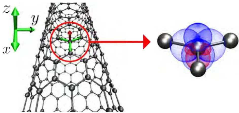
We chose a coordinate system having one carbon as origin, thexaxis parallel to the nanotube axis and thezaxis orthogonal to the tube surface, as shown in Fig. 1.4. The unit vectors along the bonds between this atom and its first neighbors can be written as:
u1 = i (1.22)
u2 = −sinθcosφi+sinθsinφj+cosθk (1.23)
u3 = −sinθcosφi−sinθsinφj+cosθk (1.24)
1.2 Hybridization 38
Figure 1.4: Bonds for a carbon atom in a(12,0)nanotube and the correspondingspδ hybrid orbitals.
The hybrid orbitals are written as:
|spδai = C1|si+C2|pxi+C3|pzi (1.25)
|spδbi = C4|si+
q
1−C42|pxi (1.26)
|spδci = C5|si+
q 1−C52
−sinθcosφ|pxi+sinθsinφ|pyi+cosθ|pzi
(1.27)
|spδdi = C5|si+
q
1−C52−sinθcosφ|pxi −sinθsinφ|pyi+cosθ|pzi
, (1.28)
with
C12= cos
2θ
2sin2θsin2φ (1.29)
C22= cos
2θ
2sin2θsin2φ (1.30)
C32=1− cos
2θ
sin2θsin2φ (1.31)
C42= cos
2φ
sin2φ (1.32)
C25= 2sin
2θsin2φ
−1
2sin2θsin2φ . (1.33)
We plot these orbitals for the(12,0) nanotube in Fig. 1.4 (corresponding toθ ≈96.486◦ and
φ ≈59.715◦). Here we haveC1=C2≈0.093,C3≈0.991,C4≈0.584,C5≈0.566. Note that
thespδa orbital has a strong pcharacter.
conse-quently as a function of the nanotube radiusR), we can have an idea of howδ varies withRby plotting the coefficient of|siin thespδ orbitals. In Fig. 1.5a we plotC1,C4andC5 for a(n,0)
nanotube as a function ofn.
Figure 1.5: Coefficients for thesorbital in thesp2andsp3hybridization schemes and for thespδ case
for a(n,0)nanotube (a) as a function ofnand for a CHCl3like molecule (b) as a function ofθ.
Note that as nincreases,C1 tends to zero, while bothC4andC5 go to 1/√3, which is the
value corresponding to sp2 hybridization. On the other hand, for small n, the hybridization clearly goes far away from sp2, but the result also does not resemble a sp3 scheme (with s coefficient 1/4) since the bond angles do not go to 109◦29′.
A similar picture occurs in fullerenes (Fig. 1.6a). While carbon makes three bonds (asp2
Figure 1.6: Bonds for a carbon atom in a C60 fullerene (a) and thespδ hybridization for aCHCl3-like
molecule (b).
characteristic), they are not contained in a single plane (sp3 characteristic). If we choose the
1.2 Hybridization 40
atom and its first neighbors as:
u1 = sinθ1i+cosθ1k θ1≈101.4◦ (1.34)
u2 = sinθ2cosφ2i+sinθ2sinφ2j+cosθ2k θ2≈101.8◦;φ2≈124.3◦ (1.35)
u3 = sinθ3cosφ3i+sinθ3sinφ3j+cosθ3k θ3≈101.8◦;φ3≈235.7◦. (1.36)
If we make the simplification θ1= θ2 =θ3 =θ and φ3 =2φ2 =240◦ (suitable for certain
molecules such as CHCl3), we can use symmetry arguments to mix the orbitals by means of:
|spδai = C1|si+
q
1−C12|pzi (1.37)
|spδbi = C2|si+
q
1−C22sinθ|pxi+cosθ|pzi
(1.38)
|spδci = C2|si+
q
1−C22−1
2sinθ|pxi+
√
3
2 sinθ|pyi+cosθ|pzi (1.39)
|spδdi = C2|si+
q 1−C22
−12sinθ|pxi+
√3
2 sinθ|pyi+cosθ|pzi (1.40)
with
C1=
√
2
tanθ C2=
s
1−3cos2θ
3sin2θ . (1.41)
Note that asθ approachesπ/2 or 109◦29′we recover thesp2orsp3hybridization, respectively (Fig. 1.5b). For illustrative purposes, if we makeθ =102◦ we haveC1=0.301 (
q
1−C12= 0.954) andC2=0.551 (
q
1−C22=0.835), so that the|spδaiorbital has a stronger|picharacter than the other|spδii,i=b,c,d(Fig. 1.6b).
1.2.5
What is so special about carbon?
What makes carbon so chemically versatile and able to form a large variety of different structures is a convenient combination of different factors in its electronic structure. Carbon has 6 electrons in its neutral condition. Its electronic distribution is given by 1s22s22p2, where the
1s2electrons are strongly bonded to the nucleus, leaving the interaction with the external world
to the four 2s22p2valence electrons. This allows carbon (in principle) to present any of thespn (n=1,2,3) hybridization schemes.
bonds, while such hybridization states becomes less favored asZ increases due to the larger s−penergy difference. As the number of different hybridization states an element can form depends on thiss−psplitting, it is directly related to how chemically rich the element is.
Figure 1.7: Energies for the 2sand 2porbitals as a function of the atomic number for the atoms in the
second row of the periodic table [2].
Turning to the case of boron, for example, we have a small s−p splitting (lower than in carbon), which favors boron to present hybrid orbitals. However, boron’s electronic distribution is given by 1s22s22p1, so that we have only three electrons eligible to form bonds and the only available hybridization states arespandsp2.
Now moving to nitrogen, we can see that it has 5 valence electrons (1s22s22p3). Even though it can present sp, sp2 or sp3 hybridizations, it has an excessive number of valence electrons that usually end up occupying one of the hybrid orbitals, lowering the number of possible bonds to other atoms. An additional issue with nitrogen is that it has a higher s−p splitting compared to boron and carbon.
While boron (nitrogen) has low (high) s−p splitting and few (many) valence electrons, nature shows that carbon is intermediate between these two properties, and in the right point so as to make carbon’s chemistry so rich. In other words, while carbon has 2sand 2porbitals close in energy (allowing for multiple hybridization schemes), it has the right number of electrons so as to take advantage of it. These are some of the reasons that make carbon so special.
Another important point in the electronic structure of carbon is the absence of pelectrons in the core, rendering carbon a small atomic radius. This is another important factor that allows carbon atoms to pack together in order to form linear (sp) and planar (sp2) structures as carbon
1.3 Carbon nanotubes 42
with carbon and eventual pi-bonds are not strong enough to produce stable linear and planar geometries in silicon based structures. In other words, silicon preferably forms longer bonds, favoringsp3 hybridization. A good illustration of this aspect is the silicon doping in carbon nanotubes, where the silicon doping produces an outward local structural distortion along the radial direction [20].
In the following sections we discuss the most important carbon nanostructures and some of their related structures.
1.3
Carbon nanotubes
The post 80’s discovery of carbon nanotubes was a natural consequence of both intense research on developing highly crystaline carbon fibers [18] and the discovery of fullerenes [10]. Even though discussions over possible carbon tubular forms took place in the early 90’s [12], the true starting point of carbon nanotubes’ science is usually considered to be the work of Iijima in 1991 where the observation and resolved structure of multi-wall carbon nanotubes (MWNTs) was reported [13]. It did not take long for Iijima and Bethune to observe simultaneously (the two papers are printed back–to–back in the same issue ofNature) the existence of single-walled carbon nanotubes (SWNTs) [14, 15]. Nanotubes excited the scientific community due to a series of new interesting properties like their singular geometry–electronic structure–optical spectra relation, high mechanical resistance, chemical selectivity to chemical and physical adsorption of molecules on its surface, among others. This section is dedicated to describe some basic properties of this interesting structure.
1.3.1
Nanotube’s structure
Even though graphene is the subject of another section, we dedicate a few words to it before talking about carbon nanotubes because they are closely related to each other. Graphene is a 2D system composed by carbon atoms organized in hexagons, as a honeycomb, where the atoms present a perfect sp2 hybridization, leaving a pz (orπ) orbital free to form itinerant π bonds
(see Section 2.7). Its structure is a hexagonal 2D Bravais lattice (primitive vectorsa1 anda2)
with a 2 atom basis whose structure is depicted in Fig. 1.8a.
Figure 1.8: (a) Graphene honeycomb lattice and the vectors defining a nanotube unit cell; (b) A graphene sheet piece being rolled up to form a nanotube.
The smallest vector which is orthogonal toCh and that joins two carbon atoms is called the translational vectorT. These vectors are given by:
Ch=na1+ma2≡(n,m) (1.42)
T=t1a1+t2a2= n+2m
dr
a1−2n+m
dr
a2 (1.43)
wherenandmare integers anddr is the greatest common divisor (gcd) of 2n+mandn+2m.
In Fig. 1.8a we show these vectors for the case of a(4,1)nanotube. If we extract the rectangle
defined byChandTand roll it up (by joiningOtoAandBtoB′) we will have the nanotube’s
unit cell.
Not only the translational vector, but the whole nanotube’s geometry is determined by the (n,m)pair. In fact, the nanotube radiusRis simply determined by:
R=|Ch|/2π=a
p
n2+nm+m2 (1.44)
where a=|a1|= |a2|= aCC
√
1.3 Carbon nanotubes 44
hexagons within a nanotube unit cell (and consequently, half the number of atoms) is obtained by dividing the area of the rectangle defined byChandTby the area of an hexagon (a1·a2) [18]:
N= Ch·T a1·a2 =
2(n2+nm+m2) dr
. (1.45)
Finally, the chiralityθ (defined as the angle betweena1andCh) is given by:
θ =arccos Ch·a1
|Ch||a1|
!
=arccos 2n+m 2√n2+nm+m2
!
. (1.46)
Due to theC6 symmetry of the graphene sheet, we should restrict θ to the[0,π/6]range, or
equivalentlymto[0,n].
Two types of nanotubes are special due to their particular symmetry. Nanotubes (n,0)
and(n,n)are usually called zigzag and armchair nanotubes, respectively, due to the particular arrangement of their atoms along a section perpendicular to their axis (as shown for the(n,0)
and(n,n)in Fig. 1.9a-b). All the other nanotubes are collectively called chiral nanotubes (as the(8,2)case in Fig. 1.9c).
Figure 1.9: Examples of zigzag, armchair and chiral nanotubes.
1.3.2
Electronic structure
energy levels forπelectrons are given by
E(k) = ε±γ|f(k)|
1±s|f(k)| (1.47)
with
f(k) =1+e−ik·a1+e−ik·a2, ε=hψi
A|Hˆ|ψAii, γ =hψAi|Hˆ|ψ j
Bi, s=hψ i A|ψ
j Bi
(1.48) wherek is a vector in the graphene’s first Brillouin zone (BZ), ψi
A is the basis function
cor-responding to the A-atom labeled by i, ψBj is the basis function corresponding to the B-atom
labeled by j which is a neighbor of i, ε is the on site energy, γ is the first-neighbor hopping
integral (betweeniand any of its neighbors j) andsthe first-neighbor overlap integral. For an infinite sheet, the2D-kvector varies continuously along the reciprocal space (whose primitive vectors areb1andb2so thatbi·aj=2πδi j). We can write the reciprocal lattice vectorsK1and
K2along the chiral and translational vectors, respectively, as:
K1 = 1
N(−t2b1+t1b2) (1.49)
K2 = 1
N(mb1−nb2) (1.50)
and the vectorkis written as:
k=kc
K1
|K1|+ka
K2
|K2|, (1.51)
wherekcandkaare the vector components along the circumferential and axial directions of the
BZ, respectively. As the electronic density is confined along the nanotube circumference, the electron’s wavelengthλqis restricted to:
λq=|Ch|/q, q=0,1,2,3, ...,N−1, (1.52)
so that the vectorkis quantized along the nanotube’s circumference according to:
kc=2π/λ =2πq/|Ch| (1.53)
resulting in
k=qK1+ka
K2
|K2| (1.54)
with ka varying continuously along ]−π/|T|,π/|T|] for an infinite tube. In summary, the
1.3 Carbon nanotubes 46
Figure 1.10: Illustration of the quantum confinement along the circumferential direction in a carbon nanotube and the corresponding cutting lines over graphene’s Brillouin zone.
Since the Ch–T unit cell is larger than thea1–a2 cell, the K1–K2 cell is smaller than the
b1–b2cell. In fact, the present approach is equivalent to taking graphene’s electronic structure
over its BZ and fold it into the smaller nanotube BZ, obtaining the nanotube’s electronic band structure by the cutting lines where the zone is folded. For this reason, this model is usually referred to as zone-folding. The quantization of the reciprocal vector along the circumferential direction determines the cutting lines over graphene’s BZ so that a nanotube is metallic when a cutting line crosses aKpoint (reciprocal space point where the graphene’s valence and conduc-tion bands touch each other). One can show that this condiconduc-tion is satisfied when we have:
n−m=3i, whereiis an integer. (1.55) Furthermore we can differentiate two kinds of metallic nanotubes. Ifd=gcd(n,m), then:
• Metal 1 (M1): whenn−mis a multiple of 3, but not of 3d;
• Metal 2 (M2): whenn−mis a multiple of 3d.
These cutting lines are shown in Fig. 1.11 for the nanotubes(12,0), (6,6), (8,2)and (10,0).
Note that aKpoint is cut for the first three, while no vertice is cut in the semiconducting(10,0)
case.
For the first group, the bands cross the Fermi energy at the Γpoint (ka=0) as in the case
Figure 1.11: Cutting lines over graphene’s Brillouin zone for the nanotubes (12,0), (6,6), (8,2) and (10,0).
ka=2π/3T, like in the (6,6) and(8,2)nanotubes (Fig. 1.12b-c). In Fig. 1.12d we show the
electronic bands for the nanotube(10,0)as an example of a semiconducting tube.
Figure 1.12: Electronic band structure for the(12,0)(a),(6,6)(b),(8,2)(c) and(10,0)(d) nanotubes
obtained with the zone-folding-tight-binding method. Here we usedε=s=0. The Fermi level is at 0
eV.
It should be noticed, however, that for nanotubes with a large curvature (small radii), their hybridization deviates significantly from sp2 (as explained in Section 1.2.4) and this simple model does not give good results. As an example the(5,0)nanotube (which should be
1.4 Graphene and graphitic ribbons 48
1.4
Graphene and graphitic ribbons
Even though graphite is an abundant and well-known material, the isolation and measure-ments of individual graphene sheets was only accomplished in 2004 [16]. This result marked the starting point of a boom in the scientific publications based on both experimental and the-oretical investigation of this structure, making graphene a pop star in materials science. As stated in the last section, graphene’s structure is composed of a bidimensional arrangement of hexagons formed by the carbon atoms.
Graphene’s electronic structure can be satisfactorily described within the tight-binding model (see Section 2.7). If we setEF =s=0 we can write:
E(k) =±γp3+2cosk·a1+2cosk·a2+2cosk·(a1−a2). (1.56)
In Fig. 1.13 we plot this relation over the graphene’s hexagonal BZ by different methods.
Figure 1.13: Electronic band structure for the graphene over the Brillouin zone in a 3D (a) and 2D (b) representations and along the high symmetry lines (c). The Fermi level is atE=0.
A special characteristic of the E−k relation is its conic form near the K and K′ points (vertices of the BZ where the valence and conduction bands meet). Due to this local linear relation for low-energy levels, the electrons behave as massless Dirac fermions and we have the onset of Klein tunneling (where an electron can enter a potential barrier with unity transmission probability) [22]. This effect was predicted by theory for a graphene p−n junction [23] and further confirmed by experiments [24].